

Page 1
General Description
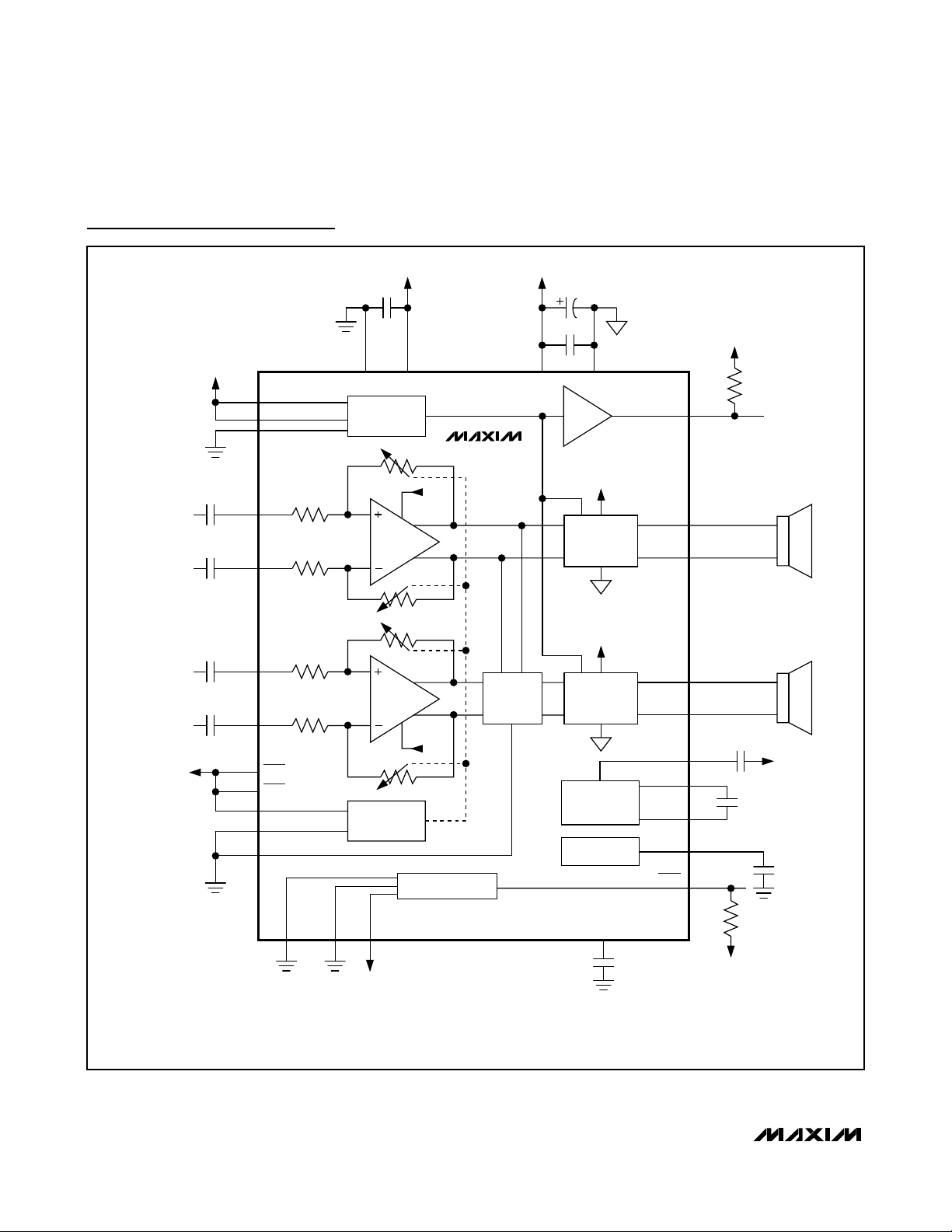
The MAX9709 stereo/mono, Class D audio power amplifier delivers up to 2 x 25W into an 8Ω stereo mode and
1 x 50W into a 4Ω load in mono mode while offering up to
87% efficiency. The MAX9709 provides Class AB amplifier performance with the benefits of Class D efficiency,
eliminating the need for a bulky heatsink and conserving
power. The MAX9709 operates from a single +10V to
+22V supply, driving the load in a BTL configuration.
The MAX9709 offers two modulation schemes: a fixed-frequency modulation (FFM) mode, and a spread-spectrum
modulation (SSM) mode that reduces EMI-radiated emissions. The MAX9709 can be synchronized to an external
clock from 600kHz to 1.2MHz. A synchronized output
allows multiple units to be cascaded in the system.
Features include fully differential inputs, comprehensive
click-and-pop suppression, and four selectable-gain settings (22dB, 25dB, 29.5dB, and 36dB). A pin-programmable thermal flag provides seven different thermal
warning thresholds. Short-circuit and thermal-overload
protection prevent the device from being damaged
during a fault condition.
The MAX9709 is available in 56-pin TQFN (8mm x 8mm
x 0.8mm) and 64-pin TQFP (10mm x 10mm x 1.4mm)
packages, and is specified over the extended
-40°C to +85°C temperature range.
Applications
LCD TVs PDP TVs
Automotive PC/HiFi Audio Solutions
Features
♦ 2 x 25W Output Power in Stereo Mode
(8Ω, THD = 10%)
♦ 1 x 50W Output Power in Mono Mode
(4Ω, THD = 10%)
♦ High Efficiency: Up to 87%
♦ Filterless Class D Amplifier
♦ Unique Patented Spread-Spectrum Mode
♦ Programmable Gain (+22dB, +25dB, +29.5dB,
+36dB)
♦ High PSRR (90dB at 1kHz)
♦ Differential Inputs Suppress Common-Mode
Noise
♦ Shutdown and Mute Control
♦ Integrated Click-and-Pop Suppression
♦ Low 0.1% THD+N
♦ Current Limit and Thermal Protection
♦ Programmable Thermal Flag
♦ Clock Synchronization Input and Output
♦ Available in Thermally Efficient, Space-Saving
Packages: 56-Pin TQFN and 64-Pin TQFP
MAX9709
25W/50W, Filterless, Spread-Spectrum,
Stereo/Mono, Class D Amplifier
________________________________________________________________ Maxim Integrated Products 1
Simplified Block Diagram
Ordering Information
19-3769; Rev 0; 9/05
For pricing, delivery, and ordering information, please contact Maxim/Dallas Direct! at
1-888-629-4642, or visit Maxim’s website at www.maxim-ic.com.
+Denotes lead-free package.
*Future product—Contact factory for availability.
**EP = Exposed paddle.
Pin Configurations appear at end of data sheet.
EVALUATION KIT
AVAILABLE
PART TEMP RANGE PIN-PACKAGE
MAX9709ETN+ -40°C to +85°C 56 TQFN-EP** T5688-3
MAX9709ECB+* -40°C to +85°C 64 TQFP-EP** C64E-6
PKG
CODE
FS1, FS2
SYNC
RIGHT
CHANNEL
LEFT
CHANNEL
MONO
G1, G2
TH0, TH1,
TH2
2
CLASS D
GAIN
CONTROL
2
MODULATOR
STEREO MODE
3
MAX9709
OUTPUT
PROTECTION
SYNCOUT
TEMP
FS1, FS2
SYNC
AUDIO
INPUT
V
G1, G2
TH0, TH1,
TH2
DIGITAL
MONO
2
CLASS D
GAIN
CONTROL
2
MODULATOR
MONO MODE
MAX9709
OUTPUT
PROTECTION
3
SYNCOUT
TEMP
Page 2
MAX9709
25W/50W, Filterless, Spread-Spectrum,
Stereo/Mono, Class D Amplifier
2 _______________________________________________________________________________________
ABSOLUTE MAXIMUM RATINGS
ELECTRICAL CHARACTERISTICS
(PVDD= VDD= +20V, PGND = GND = 0V, CSS= 0.47µF, C
REG
= 0.01µF, C1 = 0.1µF, C2 = 1µF, R
LOAD
= ∞, MONO = low (stereo
mode), SHDN = MUTE = high, G1 = low, G2 = high (A
V
= 22dB), FS1 = FS2 = high (SSM), SYNCIN = low. All load resistors (RL) are
connected between OUT_+ and OUT_-, unless otherwise stated. T
A
= T
MIN
to T
MAX
, unless otherwise noted. Typical values are at T
A
= +25°C.) (Note 1)
Stresses beyond those listed under “Absolute Maximum Ratings” may cause permanent damage to the device. These are stress ratings only, and functional
operation of the device at these or any other conditions beyond those indicated in the operational sections of the specifications is not implied. Exposure to
absolute maximum rating conditions for extended periods may affect device reliability.
PVDD, VDDto PGND, GND .......................................-0.3 to +30V
PV
DD
to VDD..........................................................-0.3V to +0.3V
OUTR+, OUTR-, OUTL+,
OUTL- to PGND, GND..........................-0.3V to (PV
DD
+ 0.3V)
C1N to GND .............................................-0.3V to (PV
DD
+ 0.3V)
C1P to GND..............................(PV
DD
- 0.3V) to (CPVDD+ 0.3V)
CPV
DD
to GND ..........................................(PV
DD
- 0.3V) to +40V
All Other Pins to GND.............................................-0.3V to +12V
Continuous Input Current (except PV
DD
, VDD, OUTR+,
OUTR-, OUTL+, and OUTL-) ..........................................20mA
Continuous Power Dissipation (T
A
= +70°C)
56-Pin Thin QFN (derate 47.6mW/°C above +70°C) .....3.81W
64-Pin TQFP (derate 43.5mW/°C above +70°C)............3.48W
Operating Temperature Range ...........................-40°C to +85°C
Storage Temperature Range .............................-65°C to +150°C
Junction Temperature......................................................+150°C
Thermal Resistance (θ
JC
)
56-Pin Thin QFN… ......................................................0.6°C/W
64-Pin TQFP…................................................................2°C/W
Lead Temperature (soldering, 10s) .................................+300°C
PARAMETER SYMBOL CONDITIONS MIN TYP MAX UNITS
Supply Voltage Range V
Shutdown Current I
Shutdown to Full Operation t
Mute to Full Operation t
Input Impedance R
Output Pulldown Resistance SHDN = GND 600 kΩ
Output Offset Voltage V
Power-Supply Rejection Ratio PSRR
Common-Mode Rejection Ratio CMRR
Switch On-Resistance R
Switching Frequency f
Oscillator Spread Bandwidth FS1 = FS2 = high (SSM) ±2 %
SYNCIN Lock Range Equal to fSW x 4 600 1200 kHz
DD
SHDN
SON
MUTE
IN
OS
DS
SW
Inferred from PSRR test 10 22 V
SHDN = low 0.1 1 µA
G1 = 0, G2 = 1 50 85 125
G1 = 1, G2 = 1 40 63 90
G1 = 1, G2 = 0 25 43 60
G1 = 0, G2 = 0 12 21 30
AC-coupled input, measured between
OUT_+ and OUT_-
PVDD = 10V to 22V 67 90
200mV
P-P
(Note 2)
DC, input referred 49 70
f = 20Hz to 20kHz, input referred 60
One power switch 0.3 0.6 Ω
FS1 FS2
0 0 180 200 220
1 1 (SSM) 200
1 0 160
0 1 250
= 1kHz 90
= 20kHz 52
ripple
f
RIPPLE
f
RIPPLE
100 ms
100 ms
3 ±40 mV
kΩ
dB
dB
kHz
Page 3
MAX9709
25W/50W, Filterless, Spread-Spectrum,
Stereo/Mono, Class D Amplifier
_______________________________________________________________________________________ 3
ELECTRICAL CHARACTERISTICS (continued)
(PVDD= VDD= +20V, PGND = GND = 0V, CSS= 0.47µF, C
REG
= 0.01µF, C1 = 0.1µF, C2 = 1µF, R
LOAD
= ∞, MONO = low (stereo
mode), SHDN = MUTE = high, G1 = low, G2 = high (A
V
= 22dB), FS1 = FS2 = high (SSM), SYNCIN = low. All load resistors (RL) are
connected between OUT_+ and OUT_-, unless otherwise stated. T
A
= T
MIN
to T
MAX
, unless otherwise noted. Typical values are at T
A
= +25°C.) (Note 1)
PARAMETER SYMBOL CONDITIONS MIN TYP MAX UNITS
Gain A
TEMP Flag Threshold T
TEMP Flag Accuracy From +80°C to +140°C ±6 °C
TEMP Flag Hysteresis 2°C
STEREO MODE (R
Quiescent Current
Output Power P
Total Harmonic Distortion Plus
Noise
Signal-to-Noise Ratio SNR P
Efficiency η P
Left-Right Channel Gain
Matching
= 8Ω, Note 3)
LOAD
V
FLAG
OUT
THD+N
G1 = 0, G2 = 1 21.6 22.0 22.3
G1 = 1, G2 = 1 24.9 25.0 25.6
G1 = 1, G2 = 0 29.2 29.5 29.9
G1 = 0, G2 = 0 35.9 36.0 36.6
TH2 TH1 TH0
000 80
001 90
0 1 0 100
0 1 1 110
1 0 0 120
1 0 1 129
1 1 0 139
111
MUTE = 1, R
MUTE = 0 6.5 13
f = 1kHz, THD =
10%, T
A
f = 1kHz, BW = 22Hz to 22kHz,
P
= 12W
OUT
= 10W
OUT
= 25W + 25W , f = 1kHz 87 %
OU T
R
= ∞ 0.2 %
LOAD
= 20V 25
= 22V 29
= 12V,
= 4Ω
22Hz to 22kHz 91
A-weighted 96
LOAD
= +25°C
= ∞ 20 33
P
VDD
P
VDD
P
VDD
R
LOAD
15
0.1 %
dB
°C
mA
W
dB
Page 4
MAX9709
25W/50W, Filterless, Spread-Spectrum,
Stereo/Mono, Class D Amplifier
4 _______________________________________________________________________________________
ELECTRICAL CHARACTERISTICS (continued)
(PVDD= VDD= +20V, PGND = GND = 0V, CSS= 0.47µF, C
REG
= 0.01µF, C1 = 0.1µF, C2 = 1µF, R
LOAD
= ∞, MONO = low (stereo
mode), SHDN = MUTE = high, G1 = low, G2 = high (A
V
= 22dB), FS1 = FS2 = high (SSM), SYNCIN = low. All load resistors (RL) are
connected between OUT_+ and OUT_-, unless otherwise stated. T
A
= T
MIN
to T
MAX
, unless otherwise noted. Typical values are at T
A
= +25°C.) (Note 1)
Note 1: All devices are 100% production tested at +25°C. All temperature limits are guaranteed by design.
Note 2: Inputs AC-coupled to GND.
Note 3: Testing performed with an 8Ω resistive load in series with a 68µH inductive load across the BTL outputs.
Note 4: Minimum output power is guaranteed by pulse testing.
Note 5: Testing performed with an 8Ω resistive load in series with a 68µH inductive load connected across BTL outputs. Mode tran-
sitions are controlled by SHDN.
Note 6: Testing performed with a 4Ω resistive load in series with a 33µH inductive load across the BTL outputs.
PARAMETER SYMBOL CONDITIONS MIN TYP MAX UNITS
Output Short-Circuit Current
Threshold
Click-and-Pop Level K
MONO MODE (R
Quiescent Current
Output Power P
Total Harmonic Distortion Plus
Noise
Signal-to-Noise Ratio SNR P
Efficiency η P
= 4Ω, MONO = HIGH) (Note 6)
LOAD
I
SC
CP
OUT
THD+N
R
LOAD
Peak voltage, 32
samples/second,
A-weighted (Notes 2, 5)
MUTE = 1, R
MUTE = 0 6.5
f = 1kHz,
THD = 10%
f = 1kHz, BW = 22Hz to 22kHz,
= 22W
P
OUT
= 10W
OUT
= 54W, f = 1kHz 86 %
OUT
= 0Ω 3A
= ∞ 20
LOAD
R
= 8Ω 25
LOAD
= 4Ω 50
R
LOAD
Into shutdown -63
Out of shutdown -55
20Hz to 20kHz 91
A-weighted 95
0.09 %
dBV
mA
W
dB
Output Short-Circuit Current
Threshold
Click-and-Pop Level K
DIGITAL INPUTS (SHDN, MUTE, G1, G2, FS1, FS2, TH0, TH1, TH2, SYNCIN, MONO)
Logic-Input Current I
Logic-Input High Voltage V
Logic-Input Low Voltage V
OPEN-DRAIN OUTPUTS (TEMP, SYNCOUT)
Open-Drain Output Low Voltage V
Leakage Current I
I
SC
CP
IN
IH
IL
OL
LEAK
R
= 0Ω 6A
LOAD
Peak voltage, 32
samples/second,
A-weighted (Notes 2, 5)
0 to 12V 1 µA
I
= 3mA 0.4 V
SINK
V
= 5.5V 0.2 µA
PULLUP
Into shutdown -60
dBV
Out of shutdown -63
2.5 V
0.8 V
Page 5
MAX9709
25W/50W, Filterless, Spread-Spectrum,
Stereo/Mono, Class D Amplifier
_______________________________________________________________________________________ 5
Typical Operating Characteristics
(PVDD= VDD= +20V, PGND = GND = 0V, CSS= 0.47µF, C
REG
= 0.01µF, C1 = 0.1µF, C2 = 1µF, R
LOAD
= 8Ω, SHDN = high, MONO
= low, MUTE = high, G1 = low, G2 = high, FS1 = FS2 = high (SSM), SYNCIN = low. All load resistors (R
L
) are between OUT_+ and
OUT_-, T
A
= +25°C, unless otherwise stated.)
SHUTDOWN SUPPLY CURRENT
vs. SUPPLY VOLTAGE
MAX9709 toc07
SUPPLY VOLTAGE (V)
SUPPLY CURRENT (nA)
201812 14 16
0.5
1.0
1.5
2.0
2.5
3.0
3.5
4.0
0
10 22
SHDN = 0
TOTAL HARMONIC DISTORTION PLUS NOISE
vs. OUTPUT POWER (MONO MODE)
MAX9709 toc08
OUTPUT POWER (W)
THD+N (%)
5040302010
0.1
1
10
100
0.01
060
R
LOAD
= 4
Ω
f
IN
= 1kHz
THD+N (%)
TOTAL HARMONIC DISTORTION PLUS NOISE
vs. OUTPUT POWER (STEREO MODE)
100
fIN = 1kHz
10
1
0.1
0.01
035
OUTPUT POWER (W)
MAX9709 toc01
30252015105
EFFICIENCY vs. OUTPUT POWER
TOTAL HARMONIC DISTORTION PLUS NOISE
vs. OUTPUT POWER (STEREO MODE)
100
PVDD = 12V
10
1
THD+N (%)
0.1
0.01
025
OUTPUT POWER vs. SUPPLY VOLTAGE
(STEREO MODE)
100
90
80
70
60
50
40
EFFICIENCY (%)
30
20
10
0
030
OUTPUT POWER (W)
252015105
MAX9709 toc04
OUTPUT POWER (W)
35
30
25
20
15
10
5
0
10 24
Ω
R
= 8
LOAD
Ω
R
= 4
LOAD
2015105
OUTPUT POWER (W)
(STEREO MODE)
THD+N = 10%
THD+N = 1%
222018161412
SUPPLY VOLTAGE (V)
MAX9709 toc02
0.1
THD+N (%)
0.01
24
22
MAX9709 toc05
20
18
16
SUPPLY CURRENT (mA)
14
12
10
TOTAL HARMONIC DISTORTION PLUS NOISE
vs. FREQUENCY (STEREO MODE)
1
P
= 12W
OUT
10 100k
NO-LOAD SUPPLY CURRENT
vs. SUPPLY VOLTAGE (STEREO MODE)
TA = +85°C
10 22
10k1k100
FREQUENCY (Hz)
TA = +25°C
TA = -40°C
2018161412
SUPPLY VOLTAGE (V)
MAX9709 toc03
MAX9709 toc06
Page 6
MAX9709
25W/50W, Filterless, Spread-Spectrum,
Stereo/Mono, Class D Amplifier
6 _______________________________________________________________________________________
Typical Operating Characteristics (continued)
(PVDD= VDD= +20V, PGND = GND = 0V, CSS= 0.47µF, C
REG
= 0.01µF, C1 = 0.1µF, C2 = 1µF, R
LOAD
= 8Ω, SHDN = high, MONO
= low, MUTE = high, G1 = low, G2 = high, FS1 = FS2 = high (SSM), SYNCIN = low. All load resistors (R
L
) are between OUT_+ and
OUT_-, T
A
= +25°C, unless otherwise stated.)
TOTAL HARMONIC DISTORTION PLUS NOISE
vs. OUTPUT POWER
MAX9709 toc09
OUTPUT POWER (W)
THD+N (%)
2015105
0.1
1
10
100
0.01
025
PVDD = 12V,
MONO MODE,
f
IN
= 1kHz
R
L
= 4
Ω
WIDEBAND OUTPUT SPECTRUM
30
20
10
0
-10
-20
-30
-40
OUTPUT AMPLITUDE (dBV)
-50
-60
-70
(FFM MODE)
FREQUENCY (Hz)
10kHz RBW
10M1M100k 100M
TOTAL HARMONIC DISTORTION PLUS NOISE
1
0.1
THD+N (%)
0.01
10 100k
0
-20
MAX9709 toc12
-40
-60
-80
OUTPUT AMPLITUDE (dBV)
-100
-120
024
vs. FREQUENCY (MONO MODE)
Ω
R
= 4
LOAD
= 22W
P
OUT
10k1k100
FREQUENCY (Hz)
OUTPUT FREQUENCY SPECTRUM
(SSM MODE)
FREQUENCY (kHz)
WIDEBAND OUTPUT SPECTRUM
(SSM MODE)
30
20
MAX9709 toc10
10
0
-10
-20
-30
-40
OUTPUT AMPLITUDE (dBV)
-50
-60
-70
100k 100M
FREQUENCY (Hz)
10kHz RBW
MAX9709 toc11
10M1M
OUTPUT FREQUENCY SPECTRUM
(FFM MODE)
0
-20
MAX9709 toc13
-40
-60
-80
OUTPUT AMPLITUDE (dBV)
-100
20161284
-120
024
FREQUENCY (kHz)
MAX9709 toc14
20161284
Page 7
MAX9709
25W/50W, Filterless, Spread-Spectrum,
Stereo/Mono, Class D Amplifier
_______________________________________________________________________________________ 7
Typical Operating Characteristics (continued)
(PVDD= VDD= +20V, PGND = GND = 0V, CSS= 0.47µF, C
REG
= 0.01µF, C1 = 0.1µF, C2 = 1µF, R
LOAD
= 8Ω, SHDN = high, MONO
= low, MUTE = high, G1 = low, G2 = high, FS1 = FS2 = high (SSM), SYNCIN = low. All load resistors (R
L
) are between OUT_+ and
OUT_-, T
A
= +25°C, unless otherwise stated.)
EFFICIENCY vs. OUTPUT POWER
OUTPUT POWER vs. SUPPLY VOLTAGE
(MONO MODE)
100
90
80
70
60
50
40
EFFICIENCY (%)
30
20
10
0
060
R
LOAD
Ω
= 4
OUTPUT POWER (W)
5040302010
70
60
MAX9709 toc15
50
40
30
OUTPUT POWER (W)
20
10
R
LOAD
= 1kHz
f
IN
0
10 24
OUTPUT POWER vs. LOAD RESISTANCE
(STEREO MODE)
30
25
THD+N = 10%
= 1kHz
f
IN
MAX9709 toc18
(MONO MODE)
Ω
= 4
THD+N = 10%
THD+N = 1%
222018161412
SUPPLY VOLTAGE (V)
MUTE RESPONSE
MAX9709 toc19
MAX9709 toc16
MUTE
5V/div
OUTPUT POWER vs. LOAD RESISTANCE
60
50
40
30
20
OUTPUT POWER (W)
10
0
412
(MONO MODE)
THD+N = 10%
= 1kHz
f
IN
1086
LOAD RESISTANCE (Ω)
SHUTDOWN RESPONSE
MAX9709 toc20
MAX9709 toc17
SHDN
5V/div
20
15
10
OUTPUT POWER PER CHANNEL (W)
5
0
716
LOAD RESISTANCE (Ω)
15141312111098
40ms/div
OUTPUT
50mV/div
40ms/div
OUTPUT
50mV/div
Page 8
MAX9709
25W/50W, Filterless, Spread-Spectrum,
Stereo/Mono, Class D Amplifier
8 _______________________________________________________________________________________
Typical Operating Characteristics (continued)
(PVDD= VDD= +20V, PGND = GND = 0V, CSS= 0.47µF, C
REG
= 0.01µF, C1 = 0.1µF, C2 = 1µF, R
LOAD
= 8Ω, SHDN = high, MONO
= low, MUTE = high, G1 = low, G2 = high, FS1 = FS2 = high (SSM), SYNCIN = low. All load resistors (R
L
) are between OUT_+ and
OUT_-, T
A
= +25°C, unless otherwise stated.)
Pin Description
COMMON-MODE REJECTION RATIO
POWER-SUPPLY REJECTION RATIO
vs. FREQUENCY
-60
INPUT REFERRED
-65
-70
-75
-80
-85
CMRR (dB)
-90
-95
-100
-105
-110
10 100k
FREQUENCY (Hz)
10k1k100
MAX9709 toc21
-30
-40
-50
-60
-70
PSRR (dB)
-80
-90
-100
-110
10 100k
vs. FREQUENCY
MAX9709 toc22
10k1k100
FREQUENCY (Hz)
-40
-50
-60
-70
-80
-90
CROSSTALK (dB)
-100
-110
-120
CROSSTALK vs. FREQUENCY
10 100k
FREQUENCY (Hz)
10k1k100
MAX9709 toc23
35
30
25
20
15
10
OUTPUT POWER PER CHANNEL (W)
5
0
PIN
TQFP TQFN
1, 8, 13, 16,
17, 32, 33, 41,
48, 49, 50, 55,
58, 63, 64
2, 3, 4, 45, 46,
47, 56, 57
5, 6, 7,
42, 43, 44
MAXIMUM STEADY-STATE OUTPUT POWER
vs. TEMPERATURE (STEREO MODE)
fIN = 1kHz
TH0 = TH1 = 1
TH2 = 0
30 70
AMBIENT TEMPERATURE (°C)
605040
NAME FUNCTION
1, 12, 42, 43,
44, 55, 56
2, 3, 4, 39,
40, 41, 49, 50
5, 6, 7,
36, 37, 38
N.C. No Connection. Not internally connected.
PGND Power Ground
PV
Positive Power Supply. Bypass to PGND with a 0.1µF and a 47µF capacitor with the
DD
smallest capacitor placed as close to pins as possible.
MAX9709 toc24
MAXIMUM STEADY-STATE OUTPUT POWER
vs. TEMPERATURE (MONO MODE)*
70
60
50
40
30
OUTPUT POWER (W)
20
R
= 4
Ω
LOAD
f
= 1kHz
IN
10
TH0 = TH1 = 1
TH2 = 0
0
30
AMBIENT TEMPERATURE (°C)
*MEASURED WITH THE MAX9709EVKIT,
JUNCTION TEMPERATURE MAINTAINED AT +110°C.
605040
MAX9709 toc25
70
Page 9

MAX9709
25W/50W, Filterless, Spread-Spectrum,
Stereo/Mono, Class D Amplifier
_______________________________________________________________________________________ 9
Pin Description (continued)
PIN
TQFP TQFN
9 8 C1N Charge-Pump Flying Capacitor C1, Negative Terminal
10 9 C1P Charge-Pump Flying Capacitor C1, Positive Terminal
11 10 CPV
12 11 SYNCOUT Open-Drain Slew-Rate-Limited Clock Output. Pullup with a 10kΩ to resistor to REG.
14 13 SYNCIN
15 14 FS2 Frequency Select 2
18 15 FS1 Frequency Select 1
19 16 INL- Left-Channel Negative Input (Stereo Mode Only)
20 17 INL+ Left-Channel Positive Input (Stereo Mode Only)
21 18 MONO
22, 23, 24 19, 20, 21 REG Internal Regulator Output Voltage (6V). Bypass with a 0.01µF capacitor to GND.
25, 26 22, 23 GND Analog Ground
27 24 SS Soft-Start. Connect a 0.47µF capacitor to GND to utilize soft-start power-up sequence.
28 25 V
29 26 INR- Right-Channel Negative Input. In mono mode, INR- is the negative input.
30 27 INR+ Right-Channel Positive Input. In mono mode, INR+ is the positive input.
31 28 G1 Gain Select input 1
34 29 G2 Gain Select input 2
35 30 SHDN
36 31 MUTE
37 32 TEMP Thermal Flag Output, Open Drain. Pullup with a 10kΩ resistor to REG.
38 33 TH2 Temperature Flag Threshold Select Input 2
39 34 TH1 Temperature Flag Threshold Select Input 1
40 35 TH0 Temperature Flag Threshold Select Input 0
51, 52 45, 46 OUTR- Right-Channel Negative Output
53, 54 47, 48 OUTR+ Right-Channel Positive Output
59, 60 51, 52 OUTL- Left-Channel Negative Output
61, 62 53, 54 OUTL+ Left-Channel Positive Output
EP EP GND Exposed Paddle. Connect to GND with multiple vias for best heat dissipation.
NAME FUNCTION
Charge-Pump Power Supply. Bypass to PVDD with a 1µF capacitor as close to pin as
DD
possible.
Clock Synchronization Input. Allows for synchronization of the internal oscillator with an
external clock.
Mono/Stereo Mode Input. Drive logic high for mono mode. Drive logic low for stereo
mode.
Analog Power Supply. Bypass to GND with a 0.1µF capacitor as close to pin as
DD
possible.
Active-Low Shutdown Input. Drive SHDN high for normal operation. Drive SHDN low to
place the device in shutdown mode.
Active-Low Mute Input. Drive logic low to place the device in mute. In mute mode,
Class D output stage is no longer switching. Drive high for normal operation. MUTE is
internally pulled up to V
with a100kΩ resistor.
REG
Page 10
MAX9709
25W/50W, Filterless, Spread-Spectrum,
Stereo/Mono, Class D Amplifier
10 ______________________________________________________________________________________
Typical Application Circuits/Functional Diagrams
Figure 1. Typical Application and Functional Diagram in Stereo Mode
LEFT
V
DIGITAL
V
+
-
+
-
CHANNEL
RIGHT
CHANNEL
DIGITAL
1µF
1µF
1µF
1µF
15 (18)
14 (15)
13 (14)
17 (20)
16 (19)
27 (30)
26 (29)
30 (35)
31 (36)
28 (31)
29 (34)
18 (21)
FS1
FS2
SYNCIN
INL+
INL-
INR+
INR-
SHDN
MUTE
G2
G1
MONO
5–7, 36–38
MUX
PV
DD
PV
DD
47µF*
PGND
PV
CLASS D
MODULATOR
AND H-BRIDGE
PV
CLASS D
MODULATOR
AND H-BRIDGE
CHARGE
PUMP
REGULATOR
2–4, 39–41, 49–50
(2–4, 45–47, 56–57)
SYNCOUT
DD
OUTL+
OUTL-
DD
OUTR+
OUTR-
CPV
DD
C1P
C1N
REG
TEMP
V
DIGITAL
10kΩ
11 (12)
53, 54 (61, 62)
51, 52 (59, 60)
47, 48 (53, 54)
45, 46 (51, 52)
C2
1µF
10 (11)
9 (10)
C1
0.1µF
8 (9)
19, 20, 21 (22, 23, 24)
32 (37)
PV
DD
C
REG
0.01µF
V
DD
0.1µF
22, 23
(25, 26)
V
GND
R
IN
R
IN
R
IN
R
IN
CONTROL
GAIN
CONTROL
DD
R
F
V
BIAS
R
F
R
F
V
BIAS
R
F
THERMAL SENSOR
(5–7, 42–44)25 (28)
MAX9709
24 (27)
SS
C
SS
0.47µF
V
DIGITAL
TH0 TH1 TH2
35 (40) 34 (39) 33 (38)
V
DIGITAL
CONFIGURATION: TQFN STEREO MODE, SSM, INTERNAL OSCILLATOR, GAIN = 22dB, THERMAL SETTING = +120°C
( ) TQFP PACKAGE
*ADDITIONAL BULK CAPACITANCE
10kΩ
Page 11

MAX9709
25W/50W, Filterless, Spread-Spectrum,
Stereo/Mono, Class D Amplifier
______________________________________________________________________________________ 11
Typical Application Circuits/Functional Diagrams (continued)
Figure 2. Typical Application and Functional Diagram in Mono Mode
AUDIO
INPUT
V
DIGITAL
V
DIGITAL
5–7, 36–38
MUX
PV
PV
DD
47µF*
0.1µF
DD
2–4, 39–41, 49–50
(2–4, 45–47, 56–57)
PGND
PV
DD
CLASS D
MODULATOR
AND H-BRIDGE
PV
DD
CLASS D
MODULATOR
AND H-BRIDGE
CHARGE
PUMP
REGULATOR
SYNCOUT
OUTL+
OUTL-
OUTR+
OUTR-
CPV
C1P
C1N
REG
TEMP
V
DIGITAL
11 (12)
53, 54 (61, 62)
51, 52 (59, 60)
47, 48 (53, 54)
45, 46 (51, 52)
10 (11)
DD
9 (10)
8 (9)
19, 20, 21 (22, 23, 24)
32 (37)
10kΩ
C2
1µF
C1
0.1µF
PV
DD
C
REG
0.01µF
V
DD
0.1µF
22, 23
V
DIGITAL
FS1
15 (18)
14 (15)
FS2
13 (14)
SYNCIN
1µF
17 (20)
16 (19)
30 (35)
31 (36)
28 (31)
29 (34)
18 (21)
INR+
INR-
SHDN
MUTE
G1
G2
MONO
+
1µF
-
(25, 26)
V
GND
R
IN
R
IN
CONTROL
GAIN
CONTROL
DD
R
F
V
BIAS
R
F
THERMAL SENSOR
(5–7, 42–44)25 (28)
MAX9709
TH0 TH1 TH2
35 (40) 34 (39) 33 (38)
V
DIGITAL
CONFIGURATION: TQFN MONO MODE, SSM, INTERNAL OSCILLATOR, GAIN = 22dB, THERMAL SETTING = +120°C
( ) TQFP PACKAGE
*ADDITIONAL BULK CAPACITANCE
24 (27)
V
DIGITAL
10kΩ
SS
C
SS
0.47µF
Page 12

MAX9709
25W/50W, Filterless, Spread-Spectrum,
Stereo/Mono, Class D Amplifier
12 ______________________________________________________________________________________
Detailed Description
The MAX9709 filterless, Class D audio power amplifier
features several improvements to switch mode amplifier technology. The MAX9709 is a two-channel, stereo
amplifier with 25W output power on each channel. The
amplifier can be configured to output 50W output
power in mono mode. The device offers Class AB performance with Class D efficiency, while occupying minimal board space. A unique filterless modulation
scheme and spread-spectrum switching mode create a
compact, flexible, low-noise, efficient audio power
amplifier. The differential input architecture reduces
common-mode noise pickup, and can be used without
input-coupling capacitors. The device can also be configured as a single-ended input amplifier.
Mono/Stereo Configuration
The MAX9709 features a mono mode that allows the
right and left channels to operate in parallel, achieving
up to 50W of output power. The mono mode is enabled
by applying logic high to MONO. In this mode, audio
signal applied to the right channel (INR+/INR-) is routed to the H-bridge of both channels, while signal
applied to the left channel (INL+/INL-) is ignored.
OUTL+ must be connected to OUTR+ and OUTL- must
be connected to OUTR- using heavy PC board traces
as close to the device as possible (see Figure 2).
When the device is placed in mono mode on a PC
board with outputs wired together, ensure that the
MONO pin can never be driven low when the device is
enabled. Driving the MONO pin low (stereo mode)
while the outputs are wired together in mono mode may
trigger the short-circuit or thermal protection or both,
and may even damage the device.
Efficiency
Efficiency of a Class D amplifier is attributed to the
region of operation of the output stage transistors. In a
Class D amplifier, the output transistors act as currentsteering switches and consume negligible additional
power. Any power loss associated with the Class D output stage is mostly due to the I2R loss of the MOSFET
on-resistance and quiescent current overhead. The
theoretical best efficiency of a linear amplifier is 78%;
however, that efficiency is only exhibited at peak output
powers. Under normal operating levels (typical music
reproduction levels), efficiency falls below 30%, whereas the MAX9709 still exhibits 87% efficiency under the
same conditions.
Shutdown
The MAX9709 features a shutdown mode that reduces
power consumption and extends battery life. Driving
SHDN low places the device in low-power (0.1µA) shutdown mode. Connect SHDN to digital high for normal
operation.
Mute Function
The MAX9709 features a clickless/popless mute mode.
When the device is muted, the outputs stop switching,
muting the speaker. Mute only affects the output stage
and does not shut down the device. To mute the
MAX9709, drive MUTE to logic low. Driving MUTE low
during the power-up/down or shutdown/turn-on cycle
optimizes click-and-pop suppression.
Click-and-Pop Suppression
The MAX9709 features comprehensive click-and-pop
suppression that eliminates audible transients on startup and shutdown. While in shutdown, the H-bridge is
pulled to GND through a 330kΩ resistor. During startup
or power-up, the input amplifiers are muted and an
internal loop sets the modulator bias voltages to the
correct levels, preventing clicks and pops when the Hbridge is subsequently enabled. Following startup, a
soft-start function gradually unmutes the input amplifiers. The value of the soft-start capacitor has an impact
on the click-and-pop levels, as well as startup time.
Thermal Sensor
The MAX9709 features an on-chip temperature sensor
that monitors the die temperature. When the junction
temperature exceeds a programmed level, TEMP is
pulled low. This flags the user to reduce power or shut
down the device. TEMP may be connected to SS or
MUTE for automatic shutdown during overheating. If
TEMP is connected to MUTE, during thermal protection
mode, the audio is muted and the device is in mute
mode. If TEMP is connected to SS, during thermal protection mode, the device is shut down but the thermal
sensor is still active.
Page 13
MAX9709
25W/50W, Filterless, Spread-Spectrum,
Stereo/Mono, Class D Amplifier
______________________________________________________________________________________ 13
TEMP returns high once the junction temperature cools
below the set threshold minus the thermal hysteresis. If
TEMP is connected to either MUTE or SS, the audio
output resumes. The temperature threshold is set by
the TH0, TH1, and TH2 inputs as shown in Table 1. An
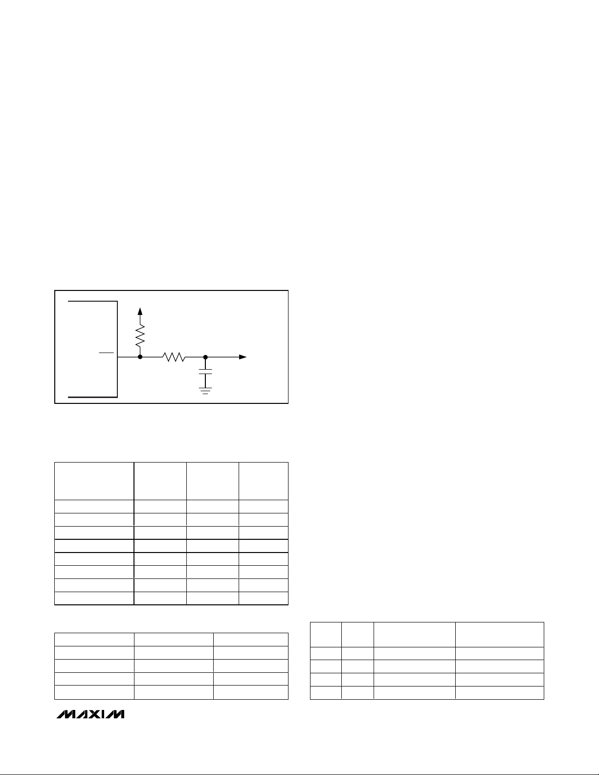
RC filter may be used to eliminate any transient at the
TEMP output as shown in Figure 3.
If TH2 = TH1 = TH0 = HIGH, it is likely that the MAX9709
enters thermal shutdown without tripping the thermal
flag.
Gain Selection
The MAX9709 features four pin-selectable gain settings;
see Table 2.
Operating Modes
Fixed-Frequency Modulation (FFM) Mode
The MAX9709 features three switching frequencies in
the FFM mode (Table 3). In this mode, the frequency
spectrum of the Class D output consists of the fundamental switching frequency and its associated harmonics (see the Wideband Output Spectrum graph in the
Typical Operating Characteristics). Select one of the
three fixed switching frequencies such that the harmonics do not fall in a sensitive band. The switching frequency can be changed any time without affecting
audio reproduction.
Spread-Spectrum Modulation (SSM) Mode
The MAX9709 features a unique, patented spreadspectrum (SSM) mode that flattens the wideband spectral components, improving EMI emissions that may be
radiated by the speaker and cables. This mode is
enabled by setting FS1 = FS2 = high. In SSM mode, the
switching frequency varies randomly by ±4% around
the center frequency (200kHz). The modulation scheme
remains the same, but the period of the triangle waveform changes from cycle to cycle. Instead of a large
amount of spectral energy present at multiples of the
switching frequency, the energy is now spread over a
bandwidth that increases with frequency. Above a few
megahertz, the wideband spectrum looks like white
noise for EMI purposes. SSM mode reduces EMI compared to fixed-frequency mode. This can also help to
randomize visual artifacts caused by radiated or supply
borne interference in displays.
Synchronous Switching Mode
The MAX9709 SYNCIN input allows the Class D amplifier to switch at a frequency defined by an external clock
frequency. Synchronizing the amplifier with an external
clock source may confine the switching frequency to a
less sensitive band. The external clock frequency range
is from 600kHz to 1.2MHz and can have any duty cycle,
but the minimum pulse must be greater than 100ns.
SYNCOUT is an open-drain clock output for synchronizing external circuitry. Its frequency is four times the
amplifier’s switching frequency and it is active in either
internal or external oscillator mode.
Figure 3. An RC Filter Eliminates Transient During Switching
Table 1. MAX9709 Junction Temperature
Threshold Setting
Table 2. MAX9709 Gain Setting
Table 3. Switching Frequencies
V
DIGITAL
10kΩ
TEMP
10kΩ
0.1µF
TO DIGITAL
INPUT
JUNCTION
TEMPERATURE
(°C)
80 Low Low Low
90 Low Low High
100 Low High Low
110 Low High High
120 High Low Low
129 High Low High
139 High High Low
158 High High High
TH2 TH1 TH0
G1 G2 GAIN (dB)
Low High 22
High High 25
High Low 29.5
Low Low 36
FS1 FS2
0 0 200 Fixed-frequency
0 1 250 Fixed-frequency
1 0 160 Fixed-frequency
1 1 200 ±4 Spread-spectrum
SYNCOUT
FREQUENCY (kHz)
MODULATION
Page 14

MAX9709
25W/50W, Filterless, Spread-Spectrum,
Stereo/Mono, Class D Amplifier
14 ______________________________________________________________________________________
Linear Regulator (REG)
The supply voltage range for the MAX9709 is from 10V
to 22V to achieve high-output power. An internal linear
regulator reduces this voltage to 6.3V for use with
small-signal and digital circuitry that does not require
high-voltage supply. Bypass a 0.01µF capacitor from
REG to GND.
Applications Information
Logic Inputs
All of the digital logic inputs and output have an
absolute maximum rating of +12V. If the MAX9709 is
operating with a supply voltage between 10V and 12V,
digital inputs can be connected to PVDDor VDD. If
PVDDand VDDare greater than 12V, digital inputs and
outputs must be connected to a digital system supply
lower than 12V.
Input Amplifier
Differential Input
The MAX9709 features a differential input structure,
making them compatible with many CODECs, and
offering improved noise immunity over a single-ended
input amplifier. In devices such as flat-panel displays,
noisy digital signals can be picked up by the amplifier’s
inputs. These signals appear at the amplifiers’ inputs as
common-mode noise. A differential input amplifier
amplifies only the difference of the two inputs, while any
signal common to both inputs is attenuated.
Single-Ended Input
The MAX9709 can be configured as a single-ended
input amplifier by capacitively coupling either input to
GND and driving the other input (Figure 4).
Component Selection
Input Filter
An input capacitor, CIN, in conjunction with the input
impedance of the MAX9709, forms a highpass filter that
removes the DC bias from an incoming signal. The ACcoupling capacitor allows the amplifier to bias the signal
to an optimum DC level. Assuming zero-source impedance, the -3dB point of the highpass filter is given by:
Choose C
IN
so that f
-3dB
is well below the lowest fre-
quency of interest. Setting f
-3dB
too high affects the
low-frequency response of the amplifier. Use capacitors with dielectrics that have low-voltage coefficients,
such as tantalum or aluminum electrolytic. Capacitors
with high-voltage coefficients, such as ceramics, may
result in increased distortion at low frequencies.
Output Filter
The MAX9709 does not require an output filter.
However, output filtering can be used if a design is failing radiated emissions due to board layout or cable
length, or the circuit is near EMI-sensitive devices. See
the MAX9709 evaluation kit for suggested filter topologies. The tuning and component selection of the filter
should be optimized for the load. A purely resistive load
(8Ω) used for lab testing requires different components
than a real, complex load-speaker load.
Charge-Pump Capacitor Selection
The MAX9709 has an internal charge-pump converter
that produces a voltage level for internal circuitry. It
requires a flying capacitor (C1) and a holding capacitor
(C2). Use capacitors with an ESR less than 100mΩ for
optimum performance. Low-ESR ceramic capacitors
minimize the output resistance of the charge pump. For
best performance over the extended temperature
range, select capacitors with an X7R dielectric. The
capacitors’ voltage rating must be greater than 36V.
Figure 4. Single-Ended Input Connections
1µF
INR+
MAX9709
f
=
dB
−
3
2 π
1
RC
IN IN
INR-
1µF
Page 15

MAX9709
25W/50W, Filterless, Spread-Spectrum,
Stereo/Mono, Class D Amplifier
______________________________________________________________________________________ 15
Sharing Input Sources
In certain systems, a single audio source can be
shared by multiple devices (speaker and headphone
amplifiers). When sharing inputs, it is common to mute
the unused device, rather than completely shutting it
down. This prevents the unused device inputs from distorting the input signal. Mute the MAX9709 by driving
MUTE low. Driving MUTE low turns off the Class D output stage, but does not affect the input bias levels of
the MAX9709.
Frequency Synchronization
The MAX9709 outputs up to 27W on each channel in
stereo mode. If higher output power or a 2.1 solution is
needed, two MAX9709s can be used. Each MAX9709
is synchronized by connecting SYNCOUT from the first
MAX9709 to SYNCIN of the second MAX9709 (see
Figure 5).
Supply Bypassing/Layout
Proper power-supply bypassing ensures low distortion
operation. For optimum performance, bypass PVDDto
PGND with a 0.1µF capacitor as close to each PV
DD
pin as possible. A low-impedance, high-current powersupply connection to PVDDis assumed. Additional bulk
capacitance should be added, as required, depending
on the application and power-supply characteristics.
GND and PGND should be star-connected to system
ground. For the TQFN package, solder the exposed
paddle (EP) to the ground plane using multiple-plated
through-hole vias. The exposed paddle must be soldered to the ground plane for rated power dissipation
and good ground return. Use wider PC board traces to
lower the parasitic resistance for the high-power output
pins (OUTR+, OUTR-, OUTL+, OUTL-). Refer to the
MAX9709 evaluation kit for layout guidance.
Thermal Considerations
Class D amplifiers provide much better efficiency and
thermal performance than a comparable Class AB
amplifier. However, the system’s thermal performance
must be considered with realistic expectations along
with its many parameters.
Continuous Sine Wave vs. Music
When a Class D amplifier is evaluated in the lab, often
a continuous sine wave is used as the signal source.
While this is convenient for measurement purposes, it
represents a worst-case scenario for thermal loading
on the amplifier. It is not uncommon for a Class D
amplifier to enter thermal shutdown if driven near maximum output power with a continuous sine wave. The
PC board must be optimized for best dissipation (see
the PC Board Thermal Considerations section).
Audio content, both music and voice, has a much lower
RMS value relative to its peak output power. Therefore,
while an audio signal may reach similar peaks as a
continuous sine wave, the actual thermal impact on the
Class D amplifier is highly reduced. If the thermal performance of a system is being evaluated, it is important
to use actual audio signals instead of sine waves for
testing. If sine waves must be used, the thermal performance is less than the system’s actual capability for
real music or voice.
PC Board Thermal Considerations
The exposed pad is the primary route for conducting
heat away from the IC. With a bottom-side exposed
pad, the PC board and its copper becomes the primary
heatsink for the Class D amplifier. Solder the exposed
pad to a copper polygon. Add as much copper as possible from this polygon to any adjacent pin on the Class
D amplifier as well as to any adjacent components, provided these connections are at the same potential.
These copper paths must be as wide as possible. Each
of these paths contributes to the overall thermal capabilities of the system.
The copper polygon to which the exposed pad is
attached should have multiple vias to the opposite side
of the PC board, where they connect to another copper
polygon. Make this polygon as large as possible within
the system’s constraints for signal routing.
Additional improvements are possible if all the traces
from the device are made as wide as possible.
Although the IC pins are not the primary thermal path
out of the package, they do provide a small amount.
The total improvement would not exceed about 10%,
but it could make the difference between acceptable
performance and thermal problems.
Page 16

MAX9709
25W/50W, Filterless, Spread-Spectrum,
Stereo/Mono, Class D Amplifier
16 ______________________________________________________________________________________
Auxiliary Heatsinking
If operating in higher ambient temperatures, it is possible
to improve the thermal performance of a PC board with
the addition of an external heatsink. The thermal resistance to this heatsink must be kept as low as possible to
maximize its performance. With a bottom-side exposed
pad, the lowest resistance thermal path is on the bottom
of the PC board. The topside of the IC is not a significant
thermal path for the device, and therefore is not a costeffective location for a heatsink. If an LC filter is used in
the design, placing the inductor in close proximity to the
IC can help draw heat away from the MAX9709.
Thermal Calculations
The die temperature of a Class D amplifier can be estimated with some basic calculations. For example, the
die temperature is calculated for the below conditions:
•T
A
= +40°C
•P
OUT
= 16W
• Efficiency (η) = 87%
• θ
JA
= 21°C/W
First, the Class D amplifier’s power dissipation must be
calculated:
Then the power dissipation is used to calculate the die
temperature, TC, as follows:
Load Impedance
The on-resistance of the MOSFET output stage in Class
D amplifiers affects both the efficiency and the peak-current capability. Reducing the peak current into the load
reduces the I
2
R losses in the MOSFETs, which increases
efficiency. To keep the peak currents lower, choose the
highest impedance speaker which can still deliver the
desired output power within the voltage swing limits of
the Class D amplifier and its supply voltage.
Another consideration is the load impedance across
the audio frequency band. A loudspeaker is a complex
electromechanical system with a variety of resonance.
In other words, an 8Ω speaker usually has 8Ω imped-
ance within a very narrow range. This often extends
well below 8Ω, reducing the thermal efficiency below
what is expected. This lower-than-expected impedance
can be further reduced when a crossover network is
used in a multidriver audio system.
Systems Application Circuit
The MAX9709 can be configured into multiple amplifier
systems. One concept is a 2.1 audio system (Figure 5)
where a stereo audio source is split into three channels.
The left- and right-channel inputs are highpass filtered
to remove the bass content, and then amplified by the
MAX9709 in stereo mode. Also, the left- and right-channel inputs are summed together and lowpass filtered to
remove the high-frequency content, then amplified by a
second MAX9709 in mono mode.
The conceptual drawing of Figure 5 can be applied to
either single-ended or differential systems. Figure 6
illustrates the circuitry required to implement a fully
differential filtering system. By maintaining a fully differential path, the signal-to-noise ratio remains uncompromised and noise pickup is kept very low. However,
keeping a fully differential signal path results in almost
twice the component count, and therefore performance
must be weighed against cost and size.
The highpass and lowpass filters should have different
cutoff frequencies to ensure an equal power response
at the crossover frequency. The filters should be at
-6dB amplitude at the crossover frequency, which is
known as a Linkwitz-Riley alignment. In the example
circuit of Figure 6, the -3dB cutoff frequency for the
highpass filters is 250Hz, and the -3dB cutoff frequency
for the lowpass filter is 160Hz. Both the highpass filters
and the lowpass filters are at a -6dB amplitude at
approximately 200Hz. If the filters were to have the
same -3dB cutoff frequency, a measurement of sound
pressure level (SPL) vs. frequency would have a peak
at the crossover frequency.
TTP C W CW C
P
P
DISS
=+ × =°+ ×° = °θ 40 24 21 90 4/.
C A DISS JA
OUT
===−−
P
η
OUT
16
W
WW
16 2 4
.
087
.
Page 17

MAX9709
25W/50W, Filterless, Spread-Spectrum,
Stereo/Mono, Class D Amplifier
______________________________________________________________________________________ 17
The circuit in Figure 6 uses inverting amplifiers for their
ease in biasing. Note the phase labeling at the outputs
has been reversed. The resistors should be 1% or better
in tolerance and the capacitors 5% tolerance or better.
Mismatch in the components can cause discrepancies
between the nominal transfer function and actual performance. Also, the mismatch of the input resistors (R15,
R17, R19, and R21 in Figure 6) of the summing amplifier
and lowpass filter causes some high-frequency sound to
be sent to the subwoofer.
The circuit in Figure 6 drives a pair of MAX9709 devices
similar to the circuit in Figure 5. The inputs to the
MAX9709 still require AC-coupling to prevent compromising the click-and-pop performance of the MAX9709.
The left and right drivers should be at an 8Ω to 12Ω
impedance, whereas the subwoofer can be 4Ω to 8Ω
depending on the desired output power, the available
power-supply voltage, and the sensitivity of the individual speakers in the system. The four gain settings of
the MAX9709 allow gain adjustments to match the sensitivity of the speakers.
Figure 5. Multiple Amplifiers Implement a 2.1 Audio System
RIGHT
AUDIO
LEFT
AUDIO
HIGHPASS
FILTER
HIGHPASS
FILTER
INR+
INR-
MONO
INL+
INL-
SYNCOUT
OUTR+
OUTR-
MAX9709
OUTL+
OUTL-
8Ω
FULLRANGE
SPEAKER
8Ω
FULLRANGE
SPEAKER
LOWPASS
Σ
FILTER
V
DIGITAL
SYNCIN
INR+
INR-
MONO
INL+
INL-
MAX9709
OUTR+
OUTR-
OUTL+
OUTL-
4Ω OR 8Ω
WOOFER
Page 18

MAX9709
25W/50W, Filterless, Spread-Spectrum,
Stereo/Mono, Class D Amplifier
18 ______________________________________________________________________________________
Figure 6. Fully Differential Crossover Filters
R1
56.2k
Ω
R2, 56.2k
U1A
MAX4478
R6, 56.2k
U1B
MAX4478
R9, 56.2k
U1C
MAX4478
R13, 56.2k
U1D
MAX4478
C9, 47nF
U2A
MAX4478
C11, 47nF
U2B
MAX4478
Ω
Ω
Ω
8
Ω
14
1
7
RIGHT
AUDIO
INPUT
LEFT
AUDIO
INPUT
NOTE:
OP AMP POWER PINS OMITTED FOR CLARITY.
ALL RESISTORS ARE 1% OR BETTER.
ALL CAPACITORS ARE 5% OR BETTER.
28k
28k
R10
28k
R14
28k
R15
26.1k
R17
26.1k
R19
26.1k
R21
28k
R3
Ω
R7
Ω
Ω
Ω
Ω
Ω
Ω
Ω
C1
47nF
C3
47nF
C5
47nF
C7
47nF
28k
28k
R11
R4
Ω
Ω
C10
47nF
7.5k
7.5k
R18
R22
C2
47nF
R5
56.2k
Ω
C4
47nF
R8
56.2k
Ω
C6
47nF
R12
56.2k
Ω
C8
47nF
R16
13k
Ω
Ω
R20
13k
Ω
Ω
BIAS
BIAS
BIAS
BIAS
BIAS
BIAS
2
3
6
5
9
10
13
12
2
3
6
5
1
RIGHT
AUDIO
OUTPUT
7
RIGHT AND LEFT OUTPUTS
ARE AC-COUPLED TO A
MAX9709 CONFIGURED AS
A STEREO AMPLIFIER
LEFT
AUDIO
OUTPUT
SUBWOOFER OUTPUT IS
AC-COUPLED TO A
MAX9709 CONFIGURED AS
A MONO AMPLIFIER
SUBWOOFER
AUDIO
OUTPUT
Page 19

MAX9709
25W/50W, Filterless, Spread-Spectrum,
Stereo/Mono, Class D Amplifier
______________________________________________________________________________________ 19
Pin Configurations
TOP VIEW
N.C.
OUTR-
OUTR-
OUTR+
OUTR+
PGND
PGND
OUTL-
OUTL-
OUTL+
OUTL+
N.C.
N.C.
DD
DD
PV
3637383940 3233343541
MAX9709
7654311109821312 141
DD
PV
DD
PV
TH0
DD
C1N
PV
PGND
PGND
PGND
PGND
PGND
DD
PV
N.C.
42
43
44
45
46
47
48
49
50
51
52
53
54
55
56
N.C.
PV
PGND
THIN QFN
TH1
C1P
TH2
DD
CPV
TEMP
SYNCOUT
MUTE
N.C.
SHDN
3031 29
SYNCIN
G2
FS2
28 G1N.C.
27
INR+
INR-
26
25
V
DD
24
SS
23
GND
GND
22
REG
21
REG
20
REG
19
MONO
18
INL+
17
INL-
16
15
FS1
Page 20

MAX9709
25W/50W, Filterless, Spread-Spectrum,
Stereo/Mono, Class D Amplifier
20 ______________________________________________________________________________________
Chip Information
PROCESS: BiCMOS
Pin Configurations (continued)
TOP VIEW
N.C.
OUTL+
OUTL+
OUTL-
OUTL-
N.C.
PGND
PGND
N.C.
OUTR+
OUTR+
OUTR-
N.C.
N.C.
64
5859606162 5455565763
OUTR-
5253
N.C.
49
5051
48 N.C.N.C.
47
46
45
44
43
42
41
40
39
38
37
36
35
34
33
PGND
PGND
PGND
PV
PV
PV
N.C.
C1N
C1P
CPV
SYNCOUT
N.C.
SYNCIN
FS2
N.C.
1
2
3
4
5
DD
6
DD
7
DD
8
9
10
11
DD
12
13
14
15
16
MAX9709
PGND
PGND
PGND
PV
DD
PV
DD
PV
DD
N.C.
TH0
TH1
TH2
TEMP
MUTE
SHDN
G2
N.C.
2322212019 2726252418 2928 32313017
DD
N.C.
FS1
INL-
INL+
MONO
REG
REG
REG
GND
GND
SS
V
INR-
INR+
G1
N.C.
TQFP
Page 21

MAX9709
25W/50W, Filterless, Spread-Spectrum,
Stereo/Mono, Class D Amplifier
______________________________________________________________________________________ 21
Package Information
(The package drawing(s) in this data sheet may not reflect the most current specifications. For the latest package outline information
go to www.maxim-ic.com/packages
.)
56L THIN QFN.EPS
PACKAGE OUTLINE
56L THIN QFN, 8x8x0.8mm
21-0135
1
E
2
Page 22

MAX9709
25W/50W, Filterless, Spread-Spectrum,
Stereo/Mono, Class D Amplifier
22 ______________________________________________________________________________________
Package Information (continued)
(The package drawing(s) in this data sheet may not reflect the most current specifications. For the latest package outline information
go to www.maxim-ic.com/packages
.)
PACKAGE OUTLINE
56L THIN QFN, 8x8x0.8mm
21-0135
2
E
2
Page 23

MAX9709
25W/50W, Filterless, Spread-Spectrum,
Stereo/Mono, Class D Amplifier
______________________________________________________________________________________ 23
Package Information (continued)
(The package drawing(s) in this data sheet may not reflect the most current specifications. For the latest package outline information
go to www.maxim-ic.com/packages
.)
64L TQFP.EPS
PACKAGE OUTLINE,
64L TQFP, 10x10x1.4mm
21-0083
1
B
2
Page 24

MAX9709
25W/50W, Filterless, Spread-Spectrum,
Stereo/Mono, Class D Amplifier
Maxim cannot assume responsibility for use of any circuitry other than circuitry entirely embodied in a Maxim product. No circuit patent licenses are
implied. Maxim reserves the right to change the circuitry and specifications without notice at any time.
24 ____________________Maxim Integrated Products, 120 San Gabriel Drive, Sunnyvale, CA 94086 408-737-7600
© 2005 Maxim Integrated Products Printed USA is a registered trademark of Maxim Integrated Products, Inc.
Quijano
Package Information (continued)
(The package drawing(s) in this data sheet may not reflect the most current specifications. For the latest package outline information
go to www.maxim-ic.com/packages
.)
Freed
PACKAGE OUTLINE,
64L TQFP, 10x10x1.4mm
21-0083
2
B
2
 Loading...