

Page 1
General Description
The MAX9703/MAX9704 mono/stereo Class D audio
power amplifiers provide Class AB amplifier performance
with Class D efficiency, conserving board space and
eliminating the need for a bulky heatsink. Using a Class
D architecture, these devices deliver up to 15W while
offering up to 78% efficiency. Proprietary and patent-protected modulation and switching schemes render the traditional Class D output filter unnecessary.
The MAX9703/MAX9704 offer two modulation schemes:
a fixed-frequency mode (FFM), and a spread-spectrum
mode (SSM) that reduces EMI-radiated emissions due
to the modulation frequency. The device utilizes a fully
differential architecture, a full bridged output, and comprehensive click-and-pop suppression.
The MAX9703/MAX9704 feature high 80dB PSRR, low
0.07% THD+N, and SNR in excess of 95dB. Short-circuit and thermal-overload protection prevent the
devices from being damaged during a fault condition.
The MAX9703 is available in a 32-pin TQFN (5mm x
5mm x 0.8mm) package. The MAX9704 is available in a
32-pin TQFN (7mm x 7mm x 0.8mm) package. Both
devices are specified over the extended -40°C to
+85°C temperature range.
Applications
Features
♦ Filterless Class D Amplifier
♦ Unique Spread-Spectrum Mode Offers 5dB
Emissions Improvement Over Conventional
Methods
♦ Up to 78% Efficient (R
L
= 8Ω)
♦ Up to 88% Efficient (R
L
= 16Ω)
♦ 15W Continuous Output Power into 8Ω (MAX9703)
♦ 2x10W Continuous Output Power into 8Ω (MAX9704)
♦ Low 0.07% THD+N
♦ High PSRR (80dB at 1kHz)
♦ 10V to 25V Single-Supply Operation
♦ Differential Inputs Minimize Common-Mode Noise
♦ Pin-Selectable Gain Reduces Component Count
♦ Industry-Leading Click-and-Pop Suppression
♦ Low Quiescent Current (24mA)
♦ Low-Power Shutdown Mode (0.2µA)
♦ Short-Circuit and Thermal-Overload Protection
♦ Available in Thermally Efficient, Space-Saving
Packages
32-Pin TQFN (5mm x 5mm x 0.8mm)–MAX9703
32-Pin TQFN (7mm x 7mm x 0.8mm)–MAX9704
MAX9703/MAX9704
10W Stereo/15W Mono, Filterless,
Spread-Spectrum, Class D Amplifiers
________________________________________________________________ Maxim Integrated Products 1
19-3160; Rev 7; 3/06
For pricing, delivery, and ordering information, please contact Maxim/Dallas Direct! at
1-888-629-4642, or visit Maxim’s website at www.maxim-ic.com.
Ordering Information
PART
AMP
PKG CODE
MAX9703ETJ+
32 TQFN-EP* Mono
T3255-3
MAX9704ETJ+
32 TQFN-EP*
T3277-2
Note: All devices specified for over -40°C to +85°C operating
temperature range.
*EP = Exposed paddle.
+Denotes lead-free package.
LCD TVs
LCD Monitors
Desktop PCs
LCD Projectors
Hands-Free Car
Phone Adaptors
Automotive
Pin Configurations appear at end of data sheet.
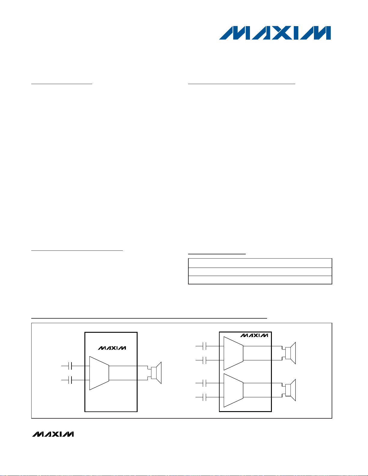
MAX9704
0.47μF
INL+ OUTL+
OUTL-INL-
0.47μF
H-BRIDGE
0.47μF
INR+ OUTR+
OUTR-INR-
0.47μF
H-BRIDGE
MAX9703
0.47μF
IN+ OUT+
OUT-
IN-
0.47μF
H-BRIDGE
Block Diagrams
PIN-PACKAGE
Stereo
Page 2
MAX9703/MAX9704
10W Stereo/15W Mono, Filterless,
Spread-Spectrum, Class D Amplifiers
2 _______________________________________________________________________________________
ABSOLUTE MAXIMUM RATINGS
Stresses beyond those listed under “Absolute Maximum Ratings” may cause permanent damage to the device. These are stress ratings only, and functional
operation of the device at these or any other conditions beyond those indicated in the operational sections of the specifications is not implied. Exposure to
absolute maximum rating conditions for extended periods may affect device reliability.
(All voltages referenced to GND.)
V
DD
to PGND, AGND .............................................................30V
OUTR_, OUTL_, C1N..................................-0.3V to (V
DD
+ 0.3V)
C1P............................................(V
DD
- 0.3V) to (CHOLD + 0.3V)
CHOLD........................................................(V
DD
- 0.3V) to +40V
All Other Pins to GND.............................................-0.3V to +12V
Duration of OUTR_/OUTL_
Short Circuit to GND, V
DD
..................................................10s
Continuous Input Current (V
DD
, PGND) ...............................1.6A
Continuous Input Current......................................................0.8A
Continuous Input Current (all other pins)..........................±20mA
Continuous Power Dissipation (T
A
= +70°C)
Single-Layer Board:
MAX9703 32-Pin TQFN (derate 21.3mW/°C
above +70°C)..........................................................1702.1mW
MAX9704 32-Pin TQFN (derate 27mW/°C
above +70°C)..........................................................2162.2mW
Multilayer Board:
MAX9703 32-Pin TQFN (derate 34.5mW/°C
above +70°C)..........................................................2758.6mW
MAX9704 32-Pin TQFN (derate 37mW/°C
above +70°C)..........................................................2963.0mW
Junction Temperature......................................................+150°C
Operating Temperature Range ...........................-40°C to +85°C
Storage Temperature Range .............................-65°C to +150°C
Lead Temperature (soldering, 10s) .................................+300°C
ELECTRICAL CHARACTERISTICS
(VDD= 15V, GND = PGND = 0V, SHDN ≥ VIH, AV= 16dB, CSS= CIN= 0.47µF, C
REG
= 0.01µF, C1 = 100nF, C2 = 1µF, FS1 = FS2 =
GND (f
S
= 660kHz), RLconnected between OUTL+ and OUTL- and OUTR+ and OUTR-, TA= T
MIN
to T
MAX
, unless otherwise noted.
Typical values are at T
A
= +25°C.) (Notes 1, 2)
PARAMETER
CONDITIONS
GENERAL
Supply Voltage Range V
DD
Inferred from PSRR test 10 25 V
MAX9703 14 22
Quiescent Current I
DD
RL = OPEN
MAX9704 24 34
Shutdown Current
0.2 1.5 µA
CSS = 470nF 100
Turn-On Time t
ON
CSS = 180nF 50
Amplifier Output Resistance in
Shutdown
SHDN = GND 150 330 kΩ
AV = 13dB 35 58 80
AV = 16dB 30 48 65
AV = 19.1dB 23 39 55
Input Impedance R
IN
AV = 29.6dB 10 15 22
kΩ
G1 = L, G2 = L
G1 = L, G2 = H
G1 = H, G2 = L
13
Voltage Gain A
V
G1 = H, G2 = H
16
dB
Gain Matching Between channels (MAX9704) 0.5 %
Output Offset Voltage V
OS
±6 ±30
Common-Mode Rejection Ratio
fIN = 1kHz, input referred 60 dB
VDD = 10V to 25V 54 80
f
RIPPLE
= 1kHz 80
Power-Supply Rejection Ratio
(Note 3)
PSRR
200mV
P-P
ripple
f
RIPPLE
= 20kHz 66
dB
SYMBOL
MIN TYP MAX UNITS
I
SHDN
CMRR
29.4 29.6 29.8
18.9 19.1 19.3
12.8
15.9
mA
ms
13.2
16.3
mV
Page 3
MAX9703/MAX9704
10W Stereo/15W Mono, Filterless,
Spread-Spectrum, Class D Amplifiers
_______________________________________________________________________________________ 3
ELECTRICAL CHARACTERISTICS (continued)
(VDD= 15V, GND = PGND = 0V, SHDN ≥ VIH, AV= 16dB, CSS= CIN= 0.47µF, C
REG
= 0.01µF, C1 = 100nF, C2 = 1µF, FS1 = FS2 =
GND (f
S
= 660kHz), RLconnected between OUTL+ and OUTL- and OUTR+ and OUTR-, TA= T
MIN
to T
MAX
, unless otherwise noted.
Typical values are at T
A
= +25°C.) (Notes 1, 2)
PARAMETER
CONDITIONS
RL = 4Ω 10
RL = 8Ω 15
Continuous Output Power
(MAX9703)
TH D + N = 10%, VDD =
16V, f = 1kH z, T
A
=
(Note 4)
18
W
RL = 4Ω 2x5
RL = 8Ω
Continuous Output Power
(MAX9704)
TH D + N = 10%, VDD =
16V, f = 1kH z, T
A
=
(Note 4)
W
Total Harmonic Distortion Plus
Noise
fIN = 1kHz, either FFM or SSM, RL = 8Ω,
P
OUT
= 4W
%
FFM 94
BW = 22Hz to
22kHz
SSM 88
FFM 97
Signal-to-Noise Ratio SNR
R
L
= 8Ω, P
OUT
=
10W, f = 1kHz
A-weighted
SSM 91
dB
Crosstalk Left to right, right to left, 8Ω load, fIN = 10kHz 65 dB
FS1 = L, FS2 = L 560 670 800
FS1 = L, FS2 = H 940
FS1 = H, FS2 = L 470
Oscillator Frequency f
OSC
FS1 = H, FS2 = H (spread-spectrum mode)
670
P
OUT
= 15W, f = 1kHz, RL = 8Ω 78
Efficiency η
P
OUT
= 10W, f = 1kHz, RL = 16Ω 88
%
Regulator Output V
REG
6V
DIGITAL INPUTS (SHDN, FS_, G_)
V
IH
2.5
Input Thresholds
V
IL
0.8
V
Input Leakage Current ±1µA
Note 1: All devices are 100% production tested at +25°C. All temperature limits are guaranteed by design.
Note 2: Testing performed with a resistive load in series with an inductor to simulate an actual speaker load. For R
L
= 8Ω, L = 68µH.
For R
L
= 4Ω, L = 33µH.
Note 3: PSRR is specified with the amplifier inputs connected to GND through C
IN
.
Note 4: The MAX9704 continuous 8Ω and 16Ω power measurements account for thermal limitations of the 32-pin TQFN-EP package.
Continuous 4Ω power measurements account for short-circuit protection of the MAX9703/MAX9704 devices.
SYMBOL
P
CONT
P
CONT
THD+N
+ 25°C , t
+ 25°C , t
CONT
CONT
= 15min
RL = 16Ω, VDD = 24V
= 15min
RL = 16Ω, VDD = 24V 2x16
MIN TYP MAX UNITS
2x10
0.07
kHz
±7%
Page 4
MAX9703/MAX9704
10W Stereo/15W Mono, Filterless,
Spread-Spectrum, Class D Amplifiers
4 _______________________________________________________________________________________
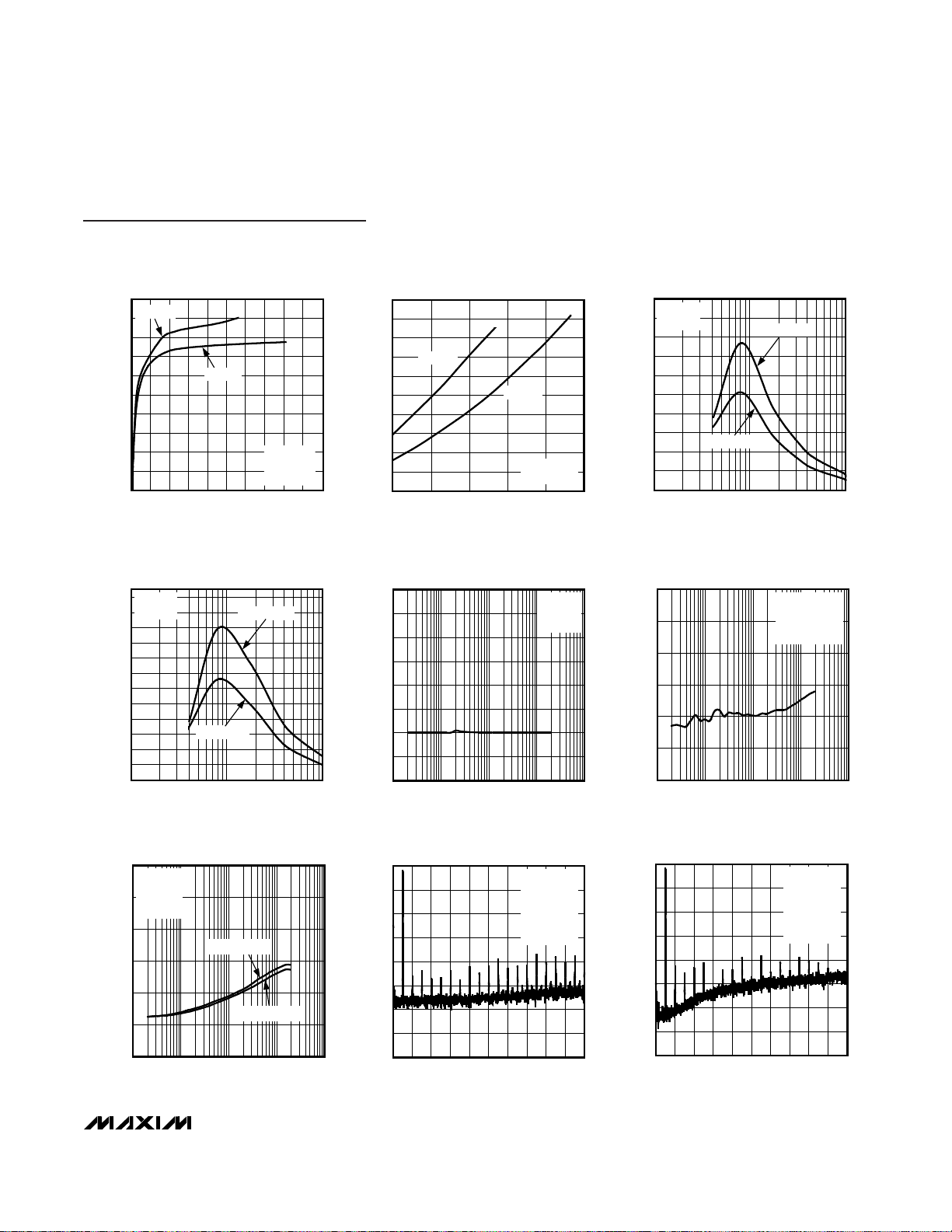
TOTAL HARMONIC DISTORTION PLUS
NOISE vs. FREQUENCY
MAX9703/04 toc01
FREQUENCY (Hz)
THD+N (%)
10k1k100
0.1
1
10
0.01
10 100k
VDD = 15V
R
L
= 4Ω
A
V
= 16dB
P
OUT
= 4W
P
OUT
= 500mW
TOTAL HARMONIC DISTORTION PLUS
NOISE vs. FREQUENCY
MAX9703/04 toc02
FREQUENCY (Hz)
THD+N (%)
10k1k100
0.1
1
10
0.01
10 100k
VDD = 15V
R
L
= 8Ω
A
V
= 16dB
P
OUT
= 500mW
P
OUT
= 8W
TOTAL HARMONIC DISTORTION PLUS
NOISE vs. FREQUENCY
MAX9703/04 toc03
FREQUENCY (Hz)
THD+N (%)
10k1k100
0.1
1
10
0.01
10 100k
VDD = 20V
R
L
= 8Ω
A
V
= 16dB
P
OUT
= 8W
P
OUT
= 500mW
TOTAL HARMONIC DISTORTION PLUS
NOISE vs. FREQUENCY
MAX9703/04 toc04
FREQUENCY (Hz)
THD+N (%)
10k1k100
0.1
1
10
0.01
10 100k
VDD = 20V
R
L
= 8Ω
A
V
= 16dB
P
OUT
= 8W
SSM
FFM
TOTAL HARMONIC DISTORTION PLUS
NOISE vs. OUTPUT POWER
MAX9703/04 toc07
OUTPUT POWER (W)
THD+N (%)
426 8 10 12 14 16 18
0.1
1
10
100
0.01
020
VDD = 20V
R
L
= 8Ω
A
V
= 16dB
f = 100Hz
f = 1kHz
f = 10kHz
TOTAL HARMONIC DISTORTION PLUS
NOISE vs. OUTPUT POWER
MAX9703/04 toc05
OUTPUT POWER (W)
THD+N (%)
6
45
231
0.1
1
10
100
0.01
010978
VDD = 15V
R
L
= 4Ω
A
V
= 16dB
f = 10kHz
f = 1kHz
f = 100Hz
TOTAL HARMONIC DISTORTION PLUS
NOISE vs. OUTPUT POWER
MAX9703/04 toc06
OUTPUT POWER (W)
THD+N (%)
12345678910 11 1213 14
0.1
1
10
0.01
015
VDD = 15V
R
L
= 8Ω
A
V
= 16dB
f = 100Hz
f = 1kHz
f = 10kHz
TOTAL HARMONIC DISTORTION PLUS
NOISE vs. OUTPUT POWER
MAX9703/04 toc08
OUTPUT POWER (W)
THD+N (%)
1234
5678
91011 12 13 141516 17 18 19
0.1
1
10
0.01
020
FFM (335kHz)
SSM
VDD = 20V
R
L
= 8Ω
A
V
= 16dB
f = 1kHz
EFFICIENCY vs. OUTPUT POWER
MAX9703/04 toc09
OUTPUT POWER (W)
EFFICIENCY (%)
86423 5 7
9
1
10
20
30
40
50
60
70
80
90
100
0
010
VDD = 12V
A
V
= 16dB
f = 1kHz
RL = 4Ω
RL = 8Ω
Typical Operating Characteristics
(33µH with 4Ω, 68µH with 8Ω, part in SSM mode, 136µH with 16Ω, measurement BW = 22Hz to 22kHz, unless otherwise noted.)
Page 5
MAX9703/MAX9704
10W Stereo/15W Mono, Filterless,
Spread-Spectrum, Class D Amplifiers
_______________________________________________________________________________________ 5
EFFICIENCY vs. OUTPUT POWER
MAX9703/04 toc10
OUTPUT POWER (W)
EFFICIENCY (%)
16
12
8
4
2
6
10
14 18
10
20
30
40
50
60
70
80
90
100
0
020
VDD = 15V
A
V
= 16dB
f = 1kHz
RL = 16Ω
RL = 8Ω
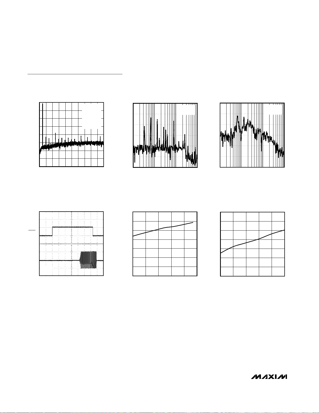
OUTPUT POWER
vs. SUPPLY VOLTAGE
MAX9703/04 toc11
SUPPLY VOLTAGE (V)
OUTPUT POWER (W)
0
6
4
2
8
10
12
14
16
18
20
10 1613 19 22 25
RL = 8Ω
RL = 16Ω
AV = 16dB
THD+N = 10%
20
18
16
14
12
10
8
6
4
2
0
110100
OUTPUT POWER
vs. LOAD RESISTANCE
MAX9703/04 toc12
LOAD RESISTANCE (Ω)
OUTPUT POWER (W)
THD+N = 1%
THD+N = 10%
VDD = 15V
A
V
= 16dB
24
22
20
18
16
14
12
10
8
6
4
2
0
1 10 100
OUTPUT POWER
vs. LOAD RESISTANCE
MAX9703/04 toc13
LOAD RESISTANCE (Ω)
OUTPUT POWER (W)
VDD = 20V
A
V
= 16dB
THD+N = 10%
THD+N = 1%
CROSSTALK vs. FREQUENCY
MAX9703/04 toc16
FREQUENCY (Hz)
CROSSTALK (dB)
10k1k100
-80
-100
-60
-40
-20
0
-120
10 100k
LEFT TO RIGHT
RIGHT TO LEFT
AV = 16dB
1% THD+N
V
DD
= 15V
8Ω LOAD
COMMON-MODE REJECTION RATIO
vs. FREQUENCY
MAX9703/04 toc14
FREQUENCY (Hz)
CMRR (dB)
10k1k100
-70
-60
-50
-40
-30
-20
-10
0
-80
10 100k
VDD = 15V
R
L
= 8Ω
A
V
= 16dB
POWER-SUPPLY REJECTION RATIO
vs. FREQUENCY
MAX9703/04 toc15
FREQUENCY (Hz)
PSRR (dB)
10k1k100
-100
-80
-60
-40
-20
0
-120
10 100k
AV = 16dB
R
L
= 8Ω
200mV
P-P
INPUT
V
DD
= 15V
OUTPUT FREQUENCY SPECTRUM
MAX9703/04 toc17
FREQUENCY (kHz)
OUTPUT MAGNITUDE (dB)
-120
-100
-80
-60
-40
-20
0
20
-140
181612 144 6 8 102020
FFM MODE
A
V
= 16dB
UNWEIGHTED
f
IN
= 1kHz
P
OUT
= 5W
R
L
= 8Ω
OUTPUT FREQUENCY SPECTRUM
MAX9703/04 toc18
FREQUENCY (kHz)
OUTPUT MAGNITUDE (dB)
-120
-100
-80
-60
-40
-20
0
20
-140
181612 144 6 8 102020
SSM MODE
A
V
= 16dB
UNWEIGHTED
f
IN
= 1kHz
P
OUT
= 5W
R
L
= 8Ω
Typical Operating Characteristics (continued)
(33µH with 4Ω, 68µH with 8Ω, part in SSM mode, 136µH with 16Ω, measurement BW = 22Hz to 22kHz, unless otherwise noted.)
Page 6
MAX9703/MAX9704
10W Stereo/15W Mono, Filterless,
Spread-Spectrum, Class D Amplifiers
6 _______________________________________________________________________________________
OUTPUT FREQUENCY SPECTRUM
MAX9703/04 toc19
FREQUENCY (kHz)
OUTPUT MAGNITUDE (dB)
-120
-100
-80
-60
-40
-20
0
20
-140
181612 144 6 8 102020
SSM MODE
A
V
= 16dB
A-WEIGHTED
f
IN
= 1kHz
P
OUT
= 5W
R
L
= 8Ω
100k 1M 10M 100M
WIDEBAND OUTPUT SPECTRUM
(FFM MODE)
MAX9703/04 toc20
FREQUENCY (Hz)
OUTPUT AMPLITUDE (dBV)
0
-120
-100
-80
-60
-40
-20
RBW = 10kHz
V
DD
= 15V
100k 1M 10M 100M
WIDEBAND OUTPUT SPECTRUM
(SSM MODE)
MAX9703/04 toc21
FREQUENCY (Hz)
OUTPUT AMPLITUDE (dBV)
0
-120
-100
-80
-60
-40
-20
RBW = 10kHz
V
DD
= 15V
TURN-ON/TURN-OFF RESPONSE
MAX9703/04 toc22
20ms/div
OUTPUT
1V/div
5V/divSHDN
f = 1kHz
R
L
= 8Ω
CSS = 180pF
SUPPLY CURRENT
vs. SUPPLY VOLTAGE
MAX9703/04 toc23
SUPPLY VOLTAGE (V)
SUPPLY CURRENT (mA)
22191613
10
5
15
20
25
30
35
0
10 25
SHUTDOWN SUPPLY CURRENT
vs. SUPPLY VOLTAGE
MAX97703/04 toc24
SUPPLY VOLTAGE (V)
SUPPLY CURRENT (μA)
18161412
0.10
0.05
0.15
0.20
0.25
0.30
0.35
0
10 20
Typical Operating Characteristics (continued)
(33µH with 4Ω, 68µH with 8Ω, part in SSM mode, 136µH with 16Ω, measurement BW = 22Hz to 22kHz, unless otherwise noted.)
Page 7

MAX9703/MAX9704
10W Stereo/15W Mono, Filterless,
Spread-Spectrum, Class D Amplifiers
_______________________________________________________________________________________ 7
PIN
MAX9703 MAX9704
NAME FUNCTION
1, 2, 23, 24 1, 2, 23, 24 PGND Power Ground
3, 4, 21, 22 3, 4, 21, 22 V
DD
Power-Supply Input
5 5 C1N Charge-Pump Flying Capacitor Negative Terminal
6 6 C1P Charge-Pump Flying Capacitor Positive Terminal
77
Charge-Pump Hold Capacitor. Connect a 1µF capacitor from CHOLD to VDD.
8, 17, 20, 25,
26, 31, 32
8 N.C. No Connection. Not internally connected.
9 14 REG 6V Internal Regulator Output. Bypass with a 0.01µF capacitor to PGND.
10 13 AGND Analog Ground
11 — IN- Negative Input
12 — IN+ Positive Input
13 12 SS
Soft-Start. Connect a 0.47µF capacitor from SS to GND to enable soft-start feature.
14 11 SHDN
Active-Low Shutdown. Connect SHDN to GND to disable the device. Connect to
V
DD
for normal operation.
15 17 G1 Gain-Select Input 1
16 18 G2 Gain-Select Input 2
18 19 FS1 Frequency-Select Input 1
19 20 FS2 Frequency-Select Input 2
27, 28 — OUT- Negative Audio Output
29, 30 — OUT+ Positive Audio Output
— 9 INL- Left-Channel Negative Input
— 10 INL+ Left-Channel Positive Input
— 15 INR- Right-Channel Negative Input
— 16 INR+ Right-Channel Positive Input
— 25, 26 OUTR- Right-Channel Negative Audio Output
— 27, 28 OUTR+ Right-Channel Positive Audio Output
— 29, 30 OUTL- Left-Channel Negative Audio Output
— 31, 32 OUTL+ Left-Channel Positive Audio Output
— — EP Exposed Paddle. Connect to GND.
Pin Description
CHOLD
Page 8

MAX9703/MAX9704
Detailed Description
The MAX9703/MAX9704 filterless, Class D audio power
amplifiers feature several improvements to switchmode amplifier technology. The MAX9703 is a mono
amplifier, the MAX9704 is a stereo amplifier. These
devices offer Class AB performance with Class D efficiency, while occupying minimal board space. A
unique filterless modulation scheme and spread-spectrum switching mode create a compact, flexible, lownoise, efficient audio power amplifier. The differential
input architecture reduces common-mode noise pickup, and can be used without input-coupling capacitors.
The devices can also be configured as a single-ended
input amplifier.
Comparators monitor the device inputs and compare
the complementary input voltages to the triangle waveform. The comparators trip when the input magnitude of
the triangle exceeds their corresponding input voltage.
Operating Modes
Fixed-Frequency Modulation (FFM) Mode
The MAX9703/MAX9704 feature three FFM modes with
different switching frequencies (Table 1). In FFM mode,
the frequency spectrum of the Class D output consists of
the fundamental switching frequency and its associated
harmonics (see the Wideband Output Spectrum (FFM
Mode) graph in the Typical Operating Characteristics).
The MAX9703/ MAX9704 allow the switching frequency to
be changed by ±35%, should the frequency of one or
more of the harmonics fall in a sensitive band. This can be
done at any time and does not affect audio reproduction.
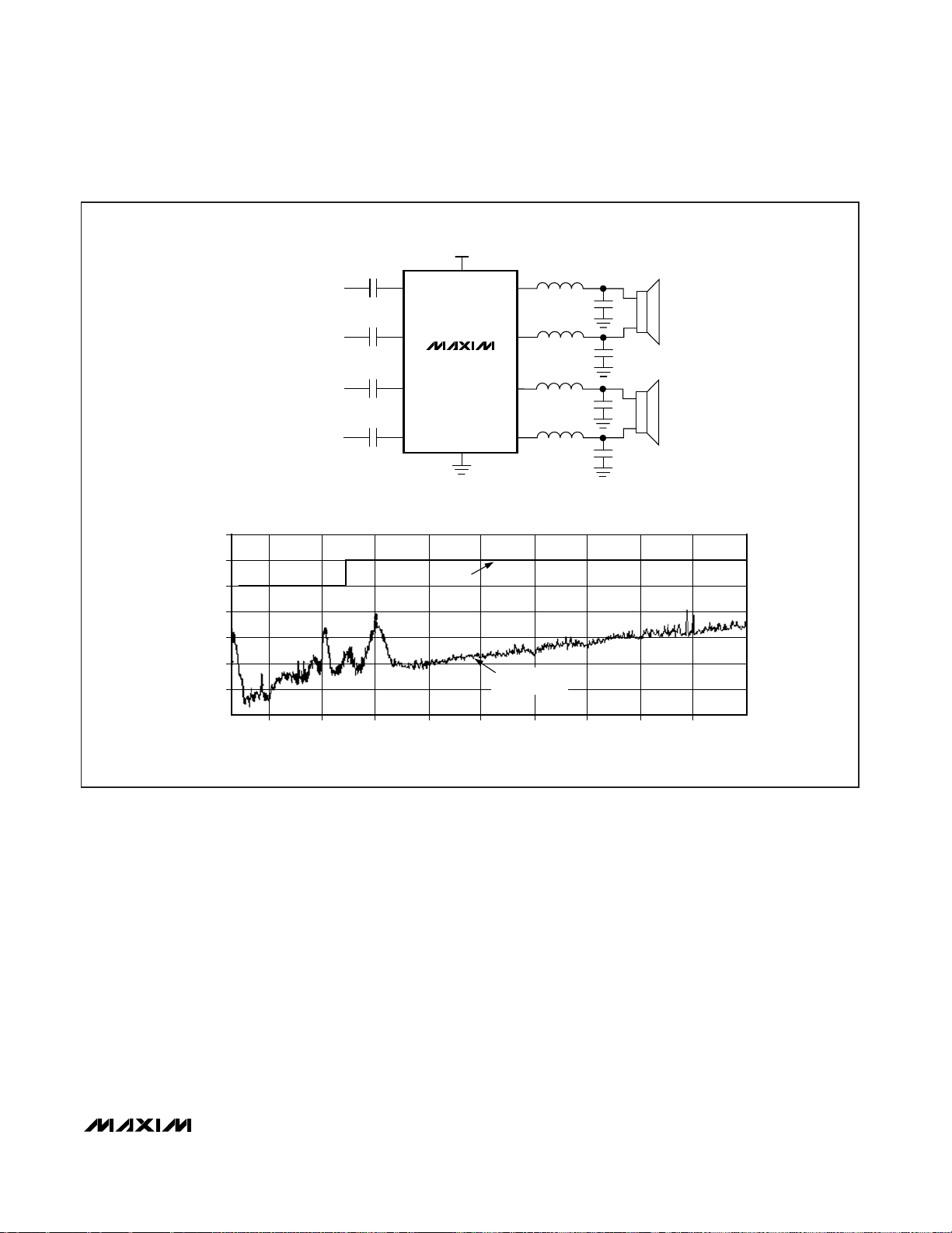
Spread-Spectrum Modulation (SSM) Mode
The MAX9703/MAX9704 feature a unique, patented
spread-spectrum mode that flattens the wideband
spectral components, improving EMI emissions that
may be radiated by the speaker and cables. This mode
is enabled by setting FS1 = FS2 = H. In SSM mode, the
switching frequency varies randomly by ±7% around
the center frequency (670kHz). The modulation scheme
remains the same, but the period of the triangle waveform changes from cycle to cycle. Instead of a large
amount of spectral energy present at multiples of the
switching frequency, the energy is now spread over a
bandwidth that increases with frequency. Above a few
megahertz, the wideband spectrum looks like white
noise for EMI purposes (see Figure 1).
Efficiency
Efficiency of a Class D amplifier is attributed to the
region of operation of the output stage transistors. In a
Class D amplifier, the output transistors act as currentsteering switches and consume negligible additional
power. Any power loss associated with the Class D output stage is mostly due to the I2R loss of the MOSFET
on-resistance, and quiescent current overhead.
The theoretical best efficiency of a linear amplifier is
78%; however, that efficiency is only exhibited at peak
output powers. Under normal operating levels (typical
music reproduction levels), efficiency falls below 30%,
whereas the MAX9704 still exhibits >78% efficiency
under the same conditions (Figure 2).
10W Stereo/15W Mono, Filterless,
Spread-Spectrum, Class D Amplifiers
8 _______________________________________________________________________________________
Table 1. Operating Modes
FS1 FS2
SWITCHING MODE
(kHz)
L L 670
L H 940
H L 470
H H 670 ±7%
Page 9
MAX9703/MAX9704
10W Stereo/15W Mono, Filterless,
Spread-Spectrum, Class D Amplifiers
_______________________________________________________________________________________ 9
Figure 1. MAX9704 EMI Spectrum, 9in PC Board trace, 3in Twisted-Pair Speaker Cable
MAX9704
V
DD
C
IN
L1*
L2*
1000pF
1000pF
L3*
L4*
1000pF
*L1–L4 = 0.05Ω DCR, 70Ω AT 100MHz, 3A FAIR RITE FERRITE BEAD (2512067007Y3).
1000pF
C
IN
C
IN
C
IN
FREQUENCY (MHz)
AMPLITUDE (dBuV/m)
900800100 200 300 500 600400 700
10
15
20
25
30
35
40
5
30 1000
CE LIMIT
MAX9704 OUTPUT
SPECTRUM
Page 10

MAX9703/MAX9704
10W Stereo/15W Mono, Filterless,
Spread-Spectrum, Class D Amplifiers
10 ______________________________________________________________________________________
Shutdown
The MAX9703/MAX9704 have a shutdown mode that
reduces power consumption and extends battery life.
Driving SHDN low places the device in low-power
(0.2µA) shutdown mode. Connect SHDN to a logic high
for normal operation.
Click-and-Pop Suppression
The MAX9703/MAX9704 feature comprehensive clickand-pop suppression that eliminates audible transients
on startup and shutdown. While in shutdown, the Hbridge is pulled to GND through 330kΩ. During startup,
or power-up, the input amplifiers are muted and an internal loop sets the modulator bias voltages to the correct
levels, preventing clicks and pops when the H-bridge is
subsequently enabled. Following startup, a soft-start
function gradually unmutes the input amplifiers. The
value of the soft-start capacitor has an impact on the
click/pop levels. For optimum performance, C
SS
should
be at least 0.18µF with a voltage rating of at least 7V.
Mute Function
The MAX9703/MA9704 features a clickless/popless
mute mode. When the device is muted, the outputs
stop switching, muting the speaker. Mute only affects
the output stage and does not shut down the device.
To mute the MAX9703/MAX9704, drive SS to GND by
using a MOSFET pulldown (Figure 3). Driving SS to
GND during the power-up/down or shutdown/turn-on
cycle optimizes click-and-pop suppression.
Applications Information
Filterless Operation
Traditional class D amplifiers require an output filter to
recover the audio signal from the amplifier’s PWM output. The filters add cost, increase the solution size of
the amplifier, and can decrease efficiency. The traditional PWM scheme uses large differential output
swings (2 ✕VDDpeak-to-peak) and causes large ripple
currents. Any parasitic resistance in the filter components results in a loss of power, lowering the efficiency.
The MAX9703/MAX9704 do not require an output filter.
The devices rely on the inherent inductance of the
speaker coil and the natural filtering of both the speaker and the human ear to recover the audio component
of the square-wave output. Eliminating the output filter
results in a smaller, less-costly, more-efficient solution.
Because the frequency of the MAX9703/MAX9704 output is well beyond the bandwidth of most speakers,
voice coil movement due to the square-wave frequency
is very small. Although this movement is small, a speaker not designed to handle the additional power can be
damaged. For optimum results, use a speaker with a
series inductance > 30µH. Typical 8Ω speakers exhibit
series inductances in the range of 30µH to 100µH.
Optimum efficiency is achieved with speaker inductances > 60µH.
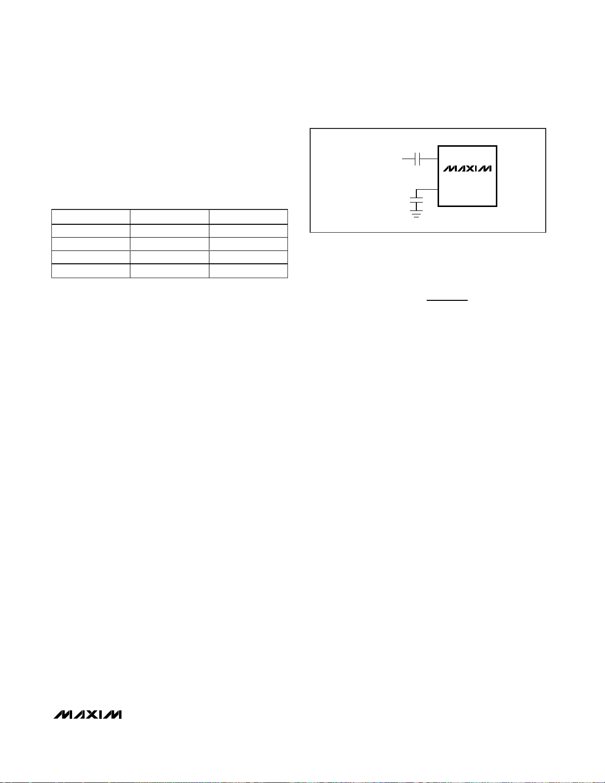
Internal Regulator Output (V
REG
)
The MAX9703/MAX9704 feature an internal, 6V regulator output (V
REG
). The MAX9703/MAX9704 REG output
pin simplifies system design and reduces system cost
by providing a logic voltage high for the MAX9703/
MAX9704 logic pins (G_, FS_). V
REG
is not available as a
logic voltage high in shutdown mode. Do not apply V
REG
as a 6V potential to surrounding system components.
Bypass REG with a 6.3V, 0.01µF capacitor to GND.
Figure 2. MAX9704 Efficiency vs. Class AB Efficiency
0
30
20
10
40
50
60
70
80
90
100
0
6
8
10 12 141618
24
20
EFFICIENCY vs. OUTPUT POWER
OUTPUT POWER (W)
EFFICIENCY (%)
VDD = 15V
f = 1kHz
R
L
= 8Ω
MAX9704
CLASS AB
Figure 3. MAX9703/MAX9704 Mute Circuit
GPIO
MUTE SIGNAL
0.18μF
SS
MAX9703/
MAX9704
Page 11
MAX9703/MAX9704
10W Stereo/15W Mono, Filterless,
Spread-Spectrum, Class D Amplifiers
______________________________________________________________________________________ 11
Gain Selection
The MAX9703/MAX9704 feature an internally set, logicselectable gain. The G1 and G2 logic inputs set the
gain of the MAX9703/MAX9704 speaker amplifier
(Table 2).
Output Offset
Unlike a Class AB amplifier, the output offset voltage of
Class D amplifiers does not noticeably increase quiescent current draw when a load is applied. This is due to
the power conversion of the Class D amplifier. For
example, an 8mV DC offset across an 8Ω load results
in 1mA extra current consumption in a class AB device.
In the Class D case, an 8mV offset into 8Ω equates
to an additional power drain of 8µW. Due to the high
efficiency of the Class D amplifier, this represents an
additional quiescent current draw of: 8µW/(VDD/100 ✕ η),
which is in the order of a few microamps.
Input Amplifier
Differential Input
The MAX9703/MAX9704 feature a differential input structure, making them compatible with many CODECs, and
offering improved noise immunity over a single-ended
input amplifier. In devices such as PCs, noisy digital signals can be picked up by the amplifier’s input traces.
The signals appear at the amplifiers’ inputs as commonmode noise. A differential input amplifier amplifies the
difference of the two inputs, any signal common to both
inputs is canceled.
Single-Ended Input
The MAX9703/MAX9704 can be configured as singleended input amplifiers by capacitively coupling either
input to GND and driving the other input (Figure 4).
Component Selection
Input Filter
An input capacitor, CIN, in conjunction with the input
impedance of the MAX9703/MAX9704, forms a highpass filter that removes the DC bias from an incoming
signal. The AC-coupling capacitor allows the amplifier
to bias the signal to an optimum DC level. Assuming
zero-source impedance, the -3dB point of the highpass
filter is given by:
Choose CINso f
-3dB
is well below the lowest frequency
of interest. Setting f
-3dB
too high affects the low-frequency response of the amplifier. Use capacitors with
dielectrics that have low-voltage coefficients, such as
tantalum or aluminum electrolytic. Capacitors with highvoltage coefficients, such as ceramics, may result in
increased distortion at low frequencies.
Charge-Pump Capacitor Selection
Use capacitors with an ESR less than 100mΩ for optimum performance. Low-ESR ceramic capacitors minimize the output resistance of the charge pump. For
best performance over the extended temperature
range, select capacitors with an X7R dielectric.
Flying Capacitor (C1)
The value of the flying capacitor (C1) affects the load
regulation and output resistance of the charge pump. A
C1 value that is too small degrades the device’s ability to
provide sufficient current drive. Increasing the value of
C1 improves load regulation and reduces the chargepump output resistance to an extent. Above 1µF, the onresistance of the switches and the ESR of C1 and C2
dominate.
Hold Capacitor (C2)
The output capacitor value and ESR directly affect the ripple at CHOLD. Increasing C2 reduces output ripple.
Likewise, decreasing the ESR of C2 reduces both ripple
and output resistance. Lower capacitance values can be
used in systems with low maximum output power levels.
Output Filter
The MAX9703/MAX9704 do not require an output filter
and can pass FCC emissions standards with unshielded speaker cables. However, output filtering can be
f
RC
-3dB
IN IN
1
2=π
MAX9703/
MAX9704
IN+
IN-
0.47μF
0.47μF
SINGLE-ENDED
AUDIO INPUT
Figure 4. Single-Ended Input
Table 2. Gain Selection
G1 G2 GAIN (dB)
0 0 29.6
0 1 19.1
1013
1116
Page 12

MAX9703/MAX9704
10W Stereo/15W Mono, Filterless,
Spread-Spectrum, Class D Amplifiers
12 ______________________________________________________________________________________
used if a design is failing radiated emissions due to
board layout or cable length, or the circuit is near EMIsensitive devices. Use a ferrite bead filter when radiated frequencies above 10MHz are of concern. Use an
LC filter when radiated frequencies below 10MHz are of
concern, or when long leads connect the amplifier to
the speaker. Refer to the MAX9704 Evaluation Kit
schematic for details of this filter.
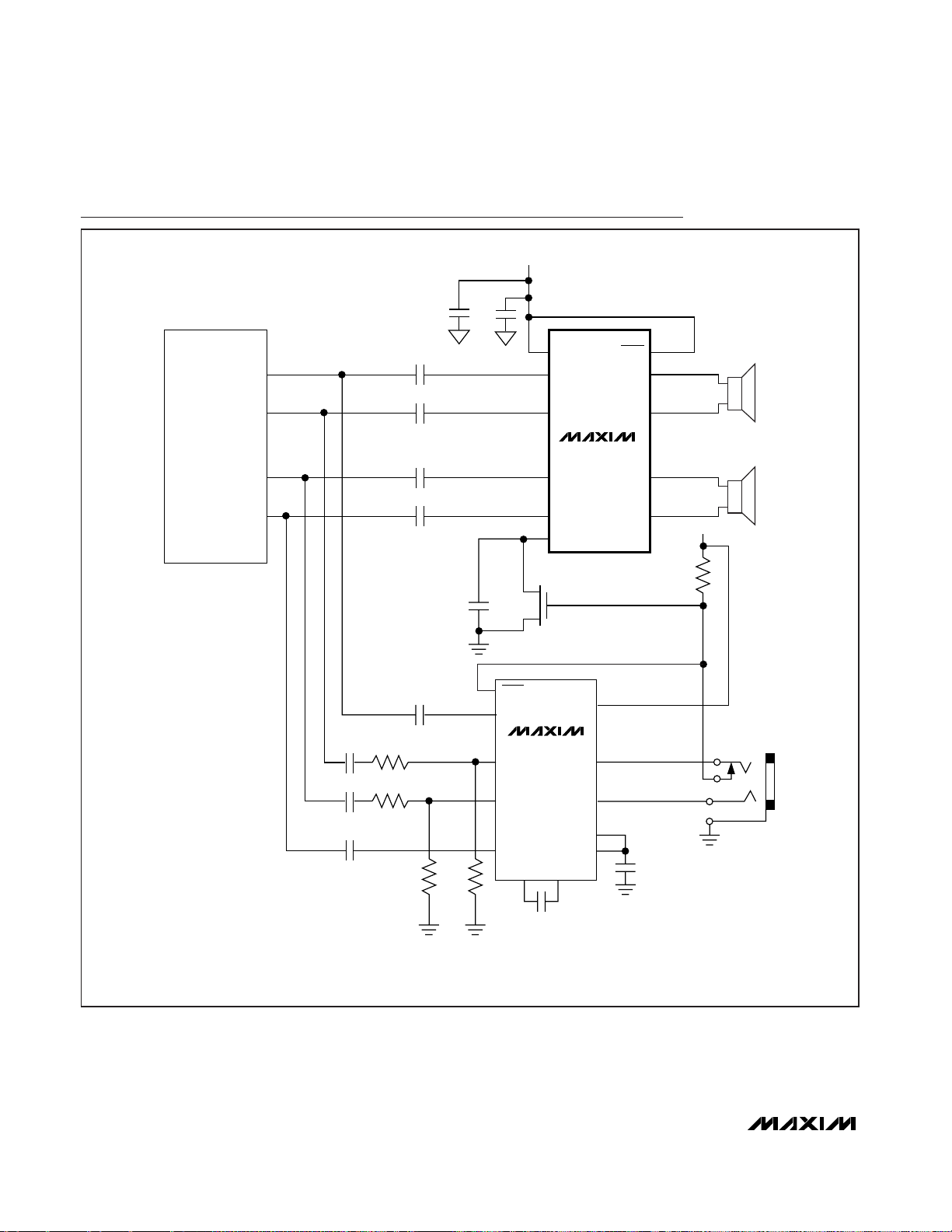
Sharing Input Sources
In certain systems, a single audio source can be shared
by multiple devices (speaker and headphone amplifiers). When sharing inputs, it is common to mute the
unused device, rather than completely shutting it down,
preventing the unused device inputs from distorting the
input signal. Mute the MAX9703/MAX9704 by driving SS
low through an open-drain output or MOSFET (see the
System Diagram). Driving SS low turns off the Class D
output stage, but does not affect the input bias levels of
the MAX9703/MAX9704. Be aware that during normal
operation, the voltage at SS can be up to 7V, depending
on the MAX9703/MAX9704 supply.
Supply Bypassing/Layout
Proper power-supply bypassing ensures low distortion
operation. For optimum performance, bypass VDDto
PGND with a 0.1µF capacitor as close to each V
DD
pin
as possible. A low-impedance, high-current power-supply connection to VDDis assumed. Additional bulk
capacitance should be added as required depending on
the application and power-supply characteristics. AGND
and PGND should be star connected to system ground.
Refer to the MAX9704 Evaluation Kit for layout guidance.
Class D Amplifier
Thermal Considerations
Class D amplifiers provide much better efficiency and
thermal performance than a comparable Class AB amplifier. However, the system’s thermal performance must be
considered with realistic expectations and include consideration of many parameters. This section examines
Class D amplifiers using general examples to illustrate
good design practices.
Continuous Sine Wave vs. Music
When a Class D amplifier is evaluated in the lab, often a
continuous sine wave is used as the signal source. While
this is convenient for measurement purposes, it represents a worst-case scenario for thermal loading on the
amplifier. It is not uncommon for a Class D amplifier to
enter thermal shutdown if driven near maximum output
power with a continuous sine wave.
Audio content, both music and voice, has a much lower
RMS value relative to its peak output power. Figure 5
shows a sine wave and an audio signal in the time
domain. Both are measured for RMS value by the oscilloscope. Although the audio signal has a slightly higher
peak value than the sine wave, its RMS value is almost
half that of the sine wave. Therefore, while an audio signal may reach similar peaks as a continuous sine wave,
the actual thermal impact on the Class D amplifier is
highly reduced. If the thermal performance of a system is
being evaluated, it is important to use actual audio signals instead of sine waves for testing. If sine waves must
be used, the thermal performance will be less than the
system’s actual capability.
PC Board Thermal Considerations
The exposed pad is the primary route of keeping heat
away from the IC. With a bottom-side exposed pad, the
PC board and its copper becomes the primary heatsink
for the Class D amplifier. Solder the exposed pad to a
large copper polygon. Add as much copper as possible
from this polygon to any adjacent pin on the Class D
amplifier as well as to any adjacent components, provided these connections are at the same potential. These
copper paths must be as wide as possible. Each of
these paths contributes to the overall thermal capabilities
of the system.
The copper polygon to which the exposed pad is
attached should have multiple vias to the opposite side
of the PC board, where they connect to another copper
polygon. Make this polygon as large as possible within
the system’s constraints for signal routing.
Figure 5. RMS Comparison of Sine Wave vs. Audio Signal
20ms/div
Page 13

MAX9703/MAX9704
10W Stereo/15W Mono, Filterless,
Spread-Spectrum, Class D Amplifiers
______________________________________________________________________________________ 13
Additional improvements are possible if all the traces
from the device are made as wide as possible. Although
the IC pins are not the primary thermal path of the package, they do provide a small amount. The total improvement would not exceed about 10%, but it could make the
difference between acceptable performance and thermal problems.
Auxiliary Heatsinking
If operating in higher ambient temperatures, it is possible
to improve the thermal performance of a PC board with
the addition of an external heatsink. The thermal resistance to this heatsink must be kept as low as possible to
maximize its performance. With a bottom-side exposed
pad, the lowest resistance thermal path is on the bottom
of the PC board. The topside of the IC is not a significant
thermal path for the device, and therefore is not a costeffective location for a heatsink.
Thermal Calculations
The die temperature of a Class D amplifier can be estimated with some basic calculations. For example, the
die temperature is calculated for the below conditions:
• TA= +40°C
• P
OUT
= 2x8W = 16W
• RL= 16Ω
• Efficiency (η) = 87%
•θJA= 27°C/W
First, the Class D amplifier’s power dissipation must be
calculated.
Then the power dissipation is used to calculate the die
temperature, TC, as follows:
TC= TA+ P
DISS
x θ
JA
= 40°C + 2.4W x 27°C/W
= 104.8°C
Decreasing the ambient temperature or reducing θ
JA
will
improve the die temperature of the MAX9704. θJAcan
be reduced by increasing the copper size/weight of the
ground plane connected to the exposed paddle of the
MAX9704 TQFN package. Additionally, θJAcan be
reduced by attaching a heatsink, adding a fan, or mounting a vertical PC board.
Load Impedance
The on-resistance of the MOSFET output stage in Class
D amplifiers affects both the efficiency and the peak-current capability. Reducing the peak current into the load
reduces the I2R losses in the MOSFETs, thereby increasing efficiency. To keep the peak currents lower, choose
the highest impedance speaker which can still deliver
the desired output power within the voltage swing limits
of the Class D amplifier and its supply voltage.
Although most loudspeakers are either 4Ω or 8Ω, there
are other impedances available which can provide a
more thermally efficient solution.
Another consideration is the load impedance across the
audio frequency band. A loudspeaker is a complex
electromechanical system with a variety of resonances.
In other words, an 8Ω speaker is usually only 8Ω imped-
ance within a very narrow range, and often extends well
below 8Ω, reducing the thermal efficiency below what is
expected. This lower-than-expected impedance can be
further reduced when a crossover network is used in a
multi-driver audio system.
Optimize MAX9704 Efficiency with
Load Impedance and Supply Voltage
To optimize the efficiency of the MAX9703/MAX9704,
load the output stage with 12Ω to 16Ω speakers. The
MAX9703/MAX9704 exhibits highest efficiency performance when driving higher load impedance (see the
Typical Operating Characteristics). If a 12Ω to 16Ω load
is not available, select a lower supply voltage when driving 6Ω to 10Ω loads.
P
P
P
W
WW
DISS
OUT
OUT
. .=−=−=
η
16
087
16 2 4
Page 14

MAX9703/MAX9704
10W Stereo/15W Mono, Filterless,
Spread-Spectrum, Class D Amplifiers
14 ______________________________________________________________________________________
MAX9703
0.47μF
LOGIC INPUTS SHOWN FOR A
V
= 16dB (SSM).
V
IN
= LOGIC HIGH > 2.5V.
†
CHOOSE CAPACITOR VOLTAGE RATING ≥ VDD.
*SYSTEM-LEVEL REQUIREMENT.
IN+
11
12
18
14
15
16
13
10 AGND
9
6
5
19
IN-
FS1
V
REG
V
REG
V
REG
V
REG
FS2
G1
G2
SS
REG
V
REG
0.47μF
MODULATOR
OSCILLATOR
CHARGE PUMP
C1P
C1
0.1μF
25V
†
C1N
0.18μF
10V
GAIN
CONTROL
SHUTDOWN
CONTROL
0.01μF
10V
SHDN
H-BRIDGE
OUT+
OUT+
OUT-
OUT-
30
29
28
27
PGND V
DD
V
DD
PGND
1 34212223242
10V TO 25V
100μF*
25V
†
0.1μF
25V
†
0.1μF
25V
†
C2
1μF
25V
†
CHOLD
V
DD
7
Functional Diagrams
Page 15

MAX9703/MAX9704
10W Stereo/15W Mono, Filterless,
Spread-Spectrum, Class D Amplifiers
______________________________________________________________________________________ 15
MAX9704
0.47μF
LOGIC INPUTS SHOWN FOR A
V
= 16dB (SSM).
V
IN
= LOGIC HIGH > 2.5V.
†
CHOOSE CAPACITOR VOLTAGE RATING ≥ VDD.
*SYSTEM-LEVEL REQUIREMENT.
INL+10
9
19
11
17
18
12
13 AGND
14
6
5
20
INL-
FS1
V
REG
V
REG
V
REG
V
REG
FS2
G1
G2
SS
REG
0.47μF
MODULATOR
OSCILLATOR
CHARGE PUMP
C1P
C1
0.1μF
25V
†
C1N
0.18μF
10V
GAIN
CONTROL
SHUTDOWN
CONTROL
0.01μF
10V
SHDN
H-BRIDGE
OUTL+
OUTL+
OUTL-
OUTL-
32
31
30
29
PGND V
DD
V
DD
PGND
1 34212223242
10V TO 25V
100μF*
25V
†
0.1μF
25V
†
0.1μF
25V
†
C2
1μF
25V
†
CHOLD
V
DD
7
0.47μF
INR+
15
16
INR-
0.47μF
MODULATOR
H-BRIDGE
OUTR+
OUTR+
OUTR-
OUTR-
28
27
26
25
V
REG
Functional Diagrams (continued)
Page 16
MAX9703/MAX9704
10W Stereo/15W Mono, Filterless,
Spread-Spectrum, Class D Amplifiers
16 ______________________________________________________________________________________
MAX9704
MAX9722B
0.47μF
V
DD
INL-
V
DD
OUTL-
SHDN
OUTL+INL+
CODEC
OUTL-
OUTL+
OUTR+
OUTR-
INR+ OUTR+
OUTR-
0.18μF
5V
V
DD
OUTL
OUTR
PV
SS
SV
SS
INL+
INL-
INR+
INR-
C1P
1μF
1μF
CIN
100kΩ
INR-
0.47μF
0.47μF
0.47μF
1μF
SS
SHDN
LOGIC INPUTS SHOWN FOR AV = 16dB (SSM).
*BULK CAPACITANCE, IF NEEDED.
1μF
30kΩ 30kΩ
15kΩ
15kΩ
1μF
1μF
1μF
100μF*
System Diagram
Page 17
MAX9703/MAX9704
10W Stereo/15W Mono, Filterless,
Spread-Spectrum, Class D Amplifiers
______________________________________________________________________________________ 17
PGND
PGND
VDDV
DD
N.C.
FS2
FS1
N.C.
PGND
PGND
VDDV
DD
C1N
CHOLD
N.C.
9
10
11
12
13
14
15
REG.
AGND
IN-
IN+
SS
SHDN
G1
32
31
30
29
28
27
26
N.C.
N.C.
OUT+
OUT+
OUT-
OUT-
N.C.
MAX9703
25
1
234 5678
24
23 22 21 20 19 18 17
N.C.
16 G2
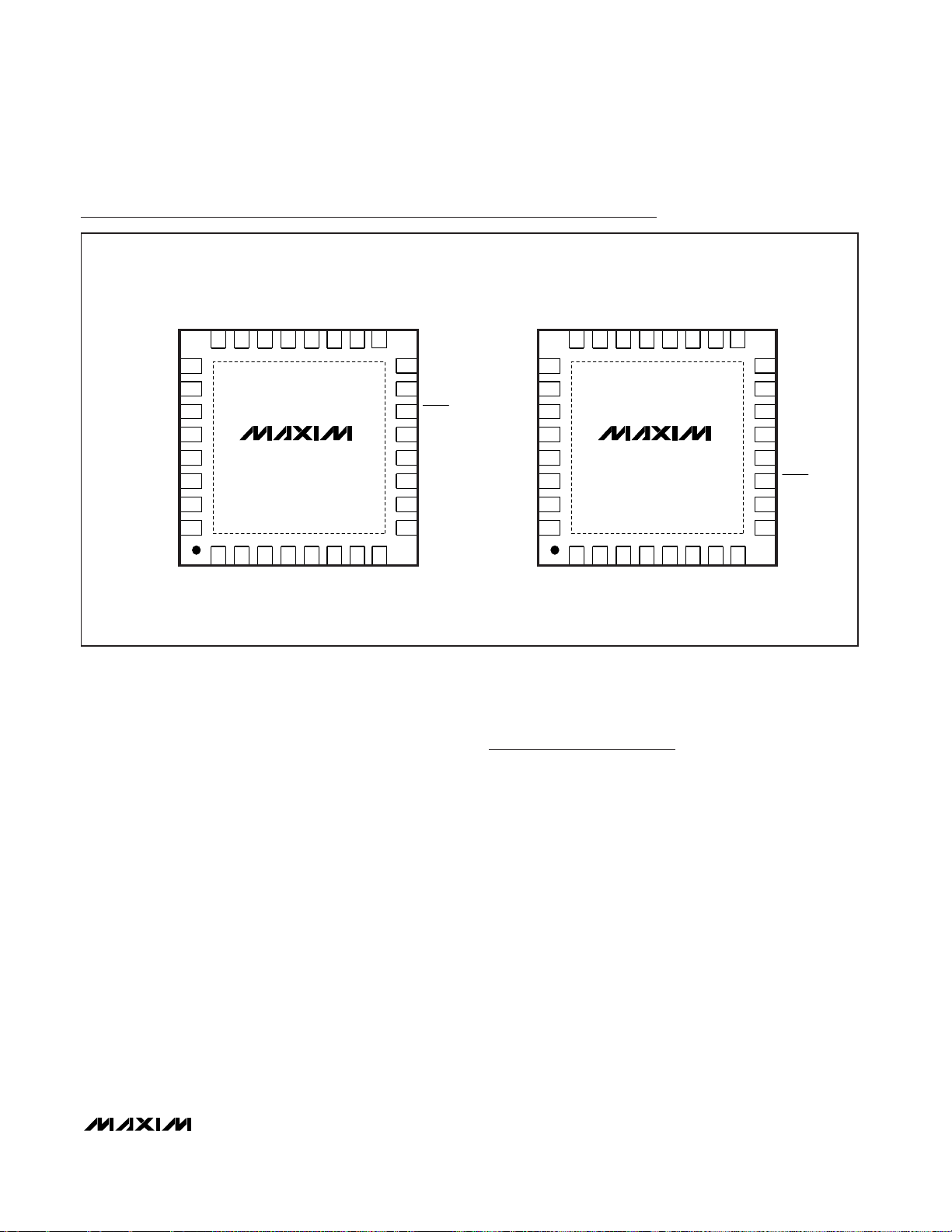
TOP VIEW
TQFN (5mm x 5mm)
C1P
TQFN (7mm x 7mm)
PGND
PGND
VDDV
DD
FS2
FS1
G2
G1
PGND
PGND
VDDV
DD
C1N
CHOLD
N.C.
9
10
11
12
13
14
15
INL-
INL+
SHDN
SS
AGND
REG.
INR-
32
31
30
29
28
27
26
OUTL+
OUTL+
OUTL-
OUTL-
OUTR+
OUTR+
OUTR-
MAX9704
25
1
234 5678
24
23 22 21 20 19 18 17
OUTR-
16 INR+
C1P
Pin Configurations
Chip Information
MAX9703 TRANSISTOR COUNT: 3093
MAX9704 TRANSISTOR COUNT: 4630
PROCESS: BiCMOS
Page 18
MAX9703/MAX9704
10W Stereo/15W Mono, Filterless,
Spread-Spectrum, Class D Amplifiers
18 ______________________________________________________________________________________
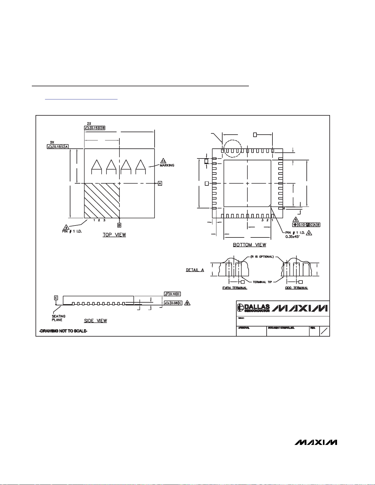
32, 44, 48L QFN
.EPS
e
L
e
L
A1AA2
E/
2
E
D/2
D
DETAIL
A
D2/2
D2
b
L
k
E2/2
E2
(NE-1) X
e
(ND-1) X
e
e
C
L
C
L
C
L
C
L
k
PACKAGE OUTLINE
21-0144
2
1
F
32, 44, 48, 56L THIN QFN, 7x7x0.8mm
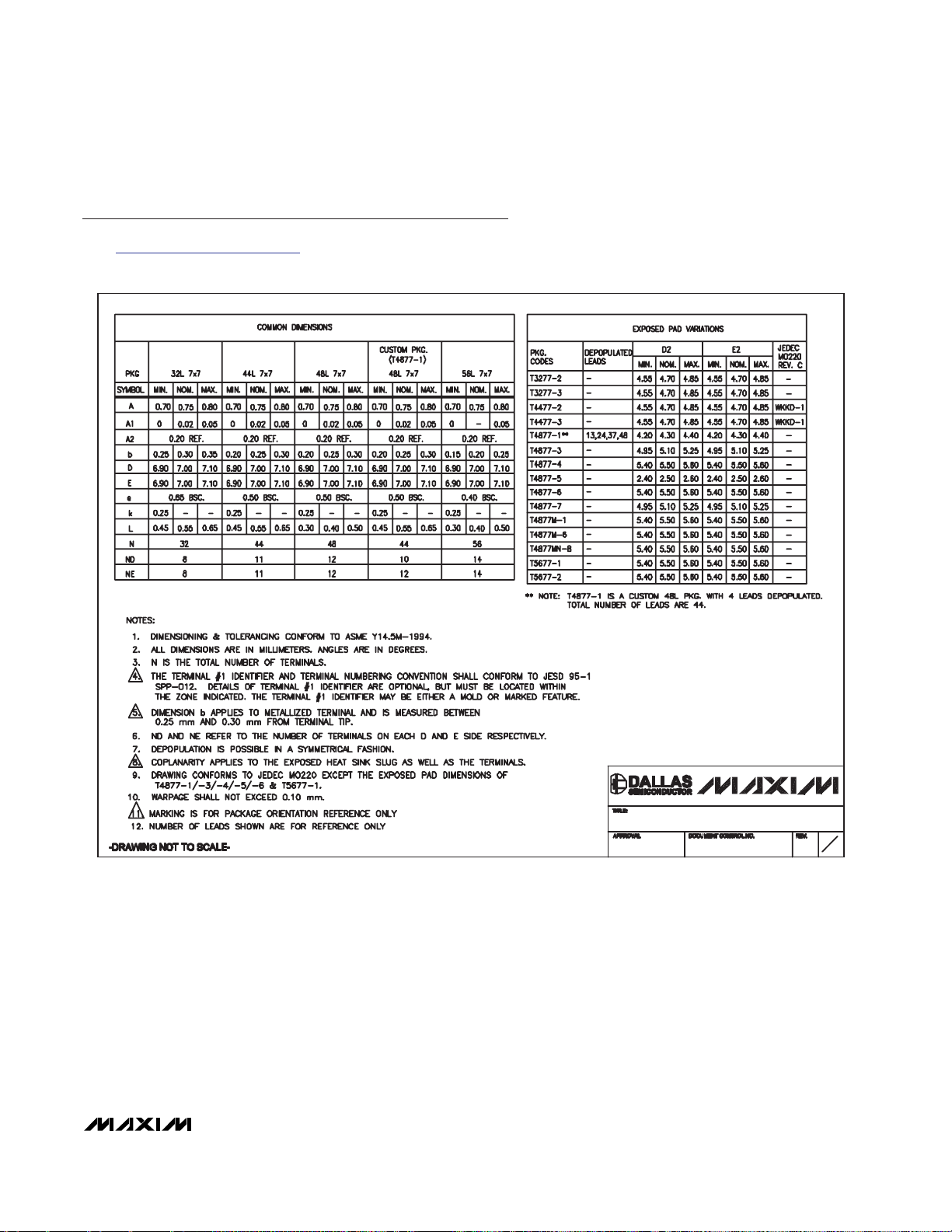
Package Information
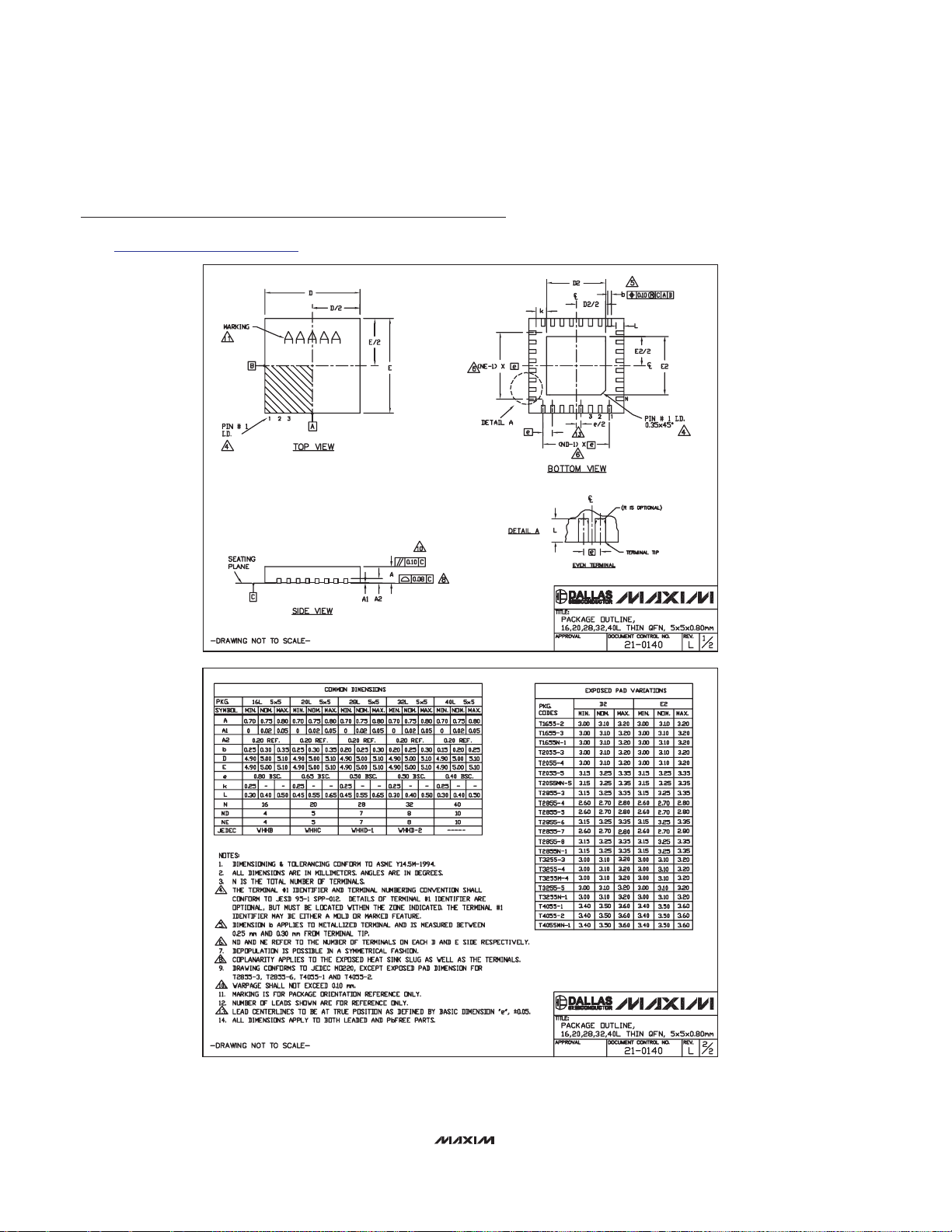
(The package drawing(s) in this data sheet may not reflect the most current specifications. For the latest package outline information,
go to www.maxim-ic.com/packages
.)
Page 19
MAX9703/MAX9704
10W Stereo/15W Mono, Filterless,
Spread-Spectrum, Class D Amplifiers
______________________________________________________________________________________ 19
PACKAGE OUTLINE
21-0144
2
2
F
32, 44, 48, 56L THIN QFN, 7x7x0.8mm
Package Information (continued)
(The package drawing(s) in this data sheet may not reflect the most current specifications. For the latest package outline information,
go to www.maxim-ic.com/packages
.)
Page 20
MAX9703/MAX9704
10W Stereo/15W Mono, Filterless,
Spread-Spectrum, Class D Amplifiers
Maxim cannot assume responsibility for use of any circuitry other than circuitry entirely embodied in a Maxim product. No circuit patent licenses are
implied. Maxim reserves the right to change the circuitry and specifications without notice at any time.
20 ____________________Maxim Integrated Products, 120 San Gabriel Drive, Sunnyvale, CA 94086 408-737-7600
© 2005 Maxim Integrated Products is a registered trademark of Maxim Integrated Products, Inc.
QFN THIN.EPS
Package Information (continued)
(The package drawing(s) in this data sheet may not reflect the most current specifications. For the latest package outline information,
go to www.maxim-ic.com/packages
.)
 Loading...