

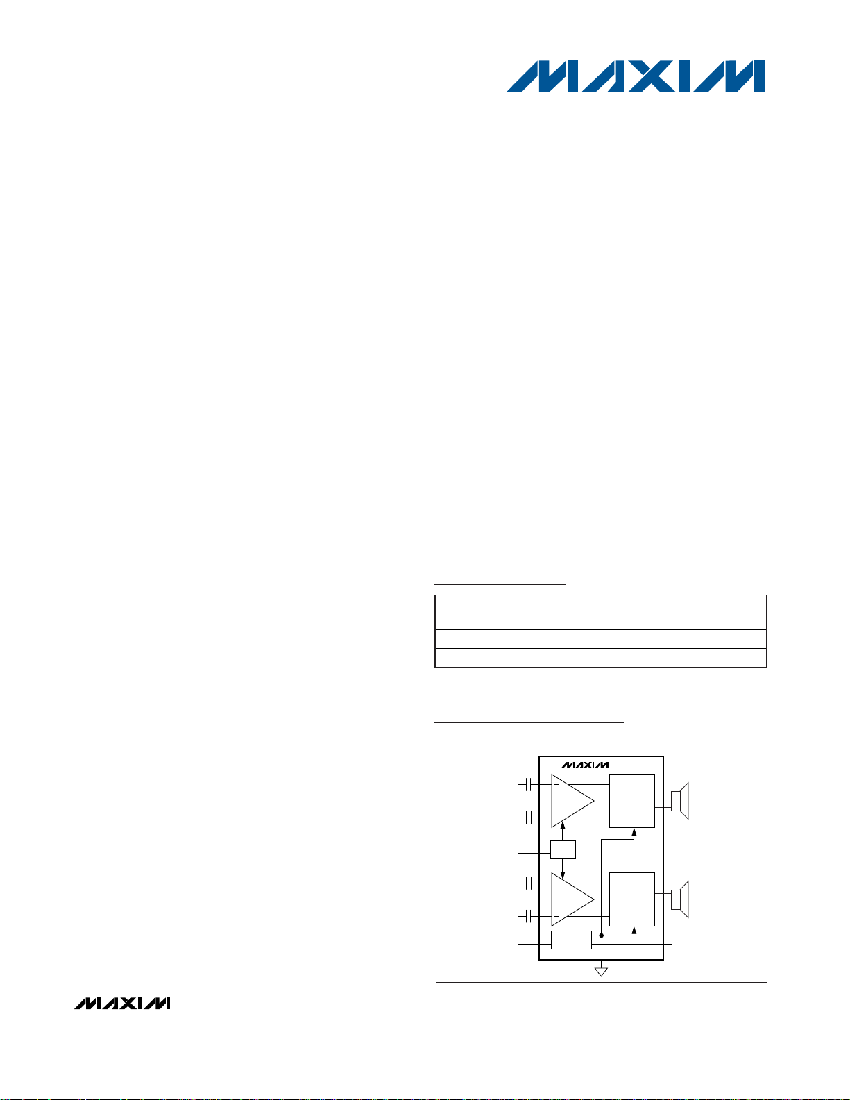
General Description
The MAX9701 stereo Class D audio power amplifier provides Class AB amplifier audio performance with the
benefits of Class D efficiency, eliminating the need for a
heatsink while extending battery life. The MAX9701
delivers up to 1.3W per channel into an 8Ω load while
offering 87% efficiency. Maxim’s next-generation, lowEMI modulation scheme allows the amplifier to operate
without an external LC filter while still meeting FCC EMI
emission levels.
The MAX9701 offers two modulation schemes: a fixed-frequency (FFM) mode, and a spread-spectrum (SSM)
mode that reduces EMI-radiated emissions. The
MAX9701 oscillator can be synchronized to an external
clock through the SYNC input, allowing synchronization of
multiple Maxim Class D amplifiers. The sync output
(SYNC_OUT) can be used for a master-slave application
where more channels are required. The MAX9701 features a fully differential architecture, a full bridge-tied load
(BTL) output, and comprehensive click-and-pop suppression. The device features internally set gains of 0dB, 6dB,
12dB, and 18dB selected through two gain-select inputs,
further reducing external component count.
The MAX9701 features high 80dB PSRR, less than 0.1%
THD+N, and SNR in excess of 88dB. Short-circuit and
thermal-overload protection prevent the device from
being damaged during a fault condition. The MAX9701 is
available in 24-pin thin QFN-EP (4mm x 4mm x 0.8mm),
and 20-bump UCSP™ (2mm x 2.5mm x 0.6mm) packages. The MAX9701 is specified over the extended
-40°C to +85°C temperature range.
Applications
Cellular Phones
Notebooks
Handheld Gaming Consoles
Docking Stations
MP3 Players
Features
♦ Patented Spread-Spectrum Modulation Lowers
Radiated Emissions
♦ Single-Supply Operation (2.5V to 5.5V)
♦ 1.3W Stereo Output (8Ω, V
DD
= 5V, THD+N = 1%)
♦ No LC Output Filter Required
♦ 87% Efficiency (R
L
= 8Ω, P
OUT
= 1000mW)
♦ Less Than 0.1% THD+N
♦ High 80dB PSRR
♦ Fully Differential Inputs
♦ Integrated Click-and-Pop Suppression
♦ Typical Low Quiescent Current (9mA)
♦ Typical Low-Power Shutdown Mode (0.1µA)
♦ Short-Circuit and Thermal-Overload Protection
♦ Available in Thermally Efficient, Space-Saving
Packages
24-Pin Thin QFN-EP (4mm x 4mm x 0.8mm)
20-Bump UCSP (2mm x 2.5mm x 0.6mm)
MAX9701
1.3W, Filterless, Stereo Class D Audio
Power Amplifier
________________________________________________________________ Maxim Integrated Products 1
MAX9701
GAIN2
GAIN1
V
DD
GAIN
RIGHT
MODULATOR
AND H-BRIDGE
SYNC
OSCILLATOR
LEFT
MODULATOR
AND H-BRIDGE
INR+
INR-
INL+
INL-
SYNC_OUT
Block Diagram
Ordering Information
19-3457; Rev 2; 2/07
For pricing, delivery, and ordering information, please contact Maxim/Dallas Direct! at
1-888-629-4642, or visit Maxim’s website at www.maxim-ic.com.
PART
TEMP RANGE
PINPACKAGE
PKG
CODE
MAX9701EBP-T
B20-1
MAX9701ETG+
T2444-4
Pin Configurations appear at end of data sheet.
UCSP is a trademark of Maxim Integrated Products, Inc.
+Denotes lead-free package.
*EP = Exposed paddle.
-40°C to +85°C
-40°C to +85°C
20 UCSP-20
24 TQFN-EP*
MAX9701
1.3W, Filterless, Stereo Class D Audio
Power Amplifier
2 _______________________________________________________________________________________
ABSOLUTE MAXIMUM RATINGS
ELECTRICAL CHARACTERISTICS
(VDD= PVDD= SHDN = 3.3V, GND = PGND = 0V, SYNC = 0V (FFM), gain = 6dB (GAIN1 = 0, GAIN2 = 1), RLconnected between
OUT+ and OUT-, R
L
= ∞, TA= T
MIN
to T
MAX
, unless otherwise noted. Typical values are at TA= +25°C.) (Notes 1, 2)
Stresses beyond those listed under “Absolute Maximum Ratings” may cause permanent damage to the device. These are stress ratings only, and functional
operation of the device at these or any other conditions beyond those indicated in the operational sections of the specifications is not implied. Exposure to
absolute maximum rating conditions for extended periods may affect device reliability.
VDDto GND..............................................................................6V
V
DD
to PVDD..........................................................-0.3V to +0.3V
PV
DD
to PGND .........................................................................6V
GND to PGND .......................................................-0.3V to +0.3V
All Other Pins to GND.................................-0.3V to (V
DD
+ 0.3V)
Continuous Current In/Out of PV
DD
, PGND, OUT_.........±800mA
Continuous Input Current (all other pins)..........................±20mA
Duration of OUT_ Short Circuit to GND or PV
DD
........Continuous
Duration of Short Circuit Between OUT+ and OUT- ......Continuous
Continuous Power Dissipation (TA= +70°C)
20-Bump UCSP (derate 10mW/°C above +70°C) ...........800mW
24-Pin Thin QFN (derate 20.8mW/°C above +70°C) ..1666.7mW
Junction Temperature......................................................+150°C
Operating Temperature Range ...........................-40°C to +85°C
Storage Temperature Range .............................-65°C to +150°C
Bump Temperature (soldering) Reflow............................+235°C
Lead Temperature (soldering, 10s) .................................+300°C
PARAMETER
SYMBOL
CONDITIONS
MIN
TYP
MAX
UNITS
GENERAL
Supply Voltage Range V
DD
Inferred from PSRR test 2.5 5.5 V
VDD = 3.3V, per channel 4.5 8
Quiescent Current I
DD
VDD = 5V, per channel 6.3 10
mA
Shutdown Current I
SHDN
0.1 10 µA
Common-Mode Rejection Ratio CMRR fIN = 1kHz 66 dB
Input Bias Voltage V
BIAS
V
Turn-On Time t
ON
40 ms
TA = +25oC
Output Offset Voltage V
OS
T
MIN
< TA < T
MAX
mV
VDD = 2.5V to 5.5V, VIN = 0V 60 80
f
RIPPLE
= 217Hz 72Power-Supply Rejection Ratio PSRR
100mV
P-P
ripple,
V
IN
= 0V
f
RIPPLE
= 20kHz 50
dB
Output Power (Note 3) P
OUT
THD+N = 1%,
T
A
= +25oC
V
DD
= 5V
mW
RL = 8Ω (P
OUT
= 300mW), f = 1kHz
Total Harmonic Distortion Plus
Noise (Note 3)
RL = 4Ω (P
OUT
= 400mW), f = 1kHz
%
FFM 86
BW = 22Hz
to 22kHz
SSM 86
FFM
Signal-to-Noise Ratio SNR V
OUT
= 1V
RMS
SSM
dB
SYNC = GND
SYNC = unconnected
Oscillator Frequency f
OSC
SYNC = V
DD
kHz
Minimum On-Time t
MIN
ns
SYNC Frequency Lock Range f
SYNC
kHz
THD+N
VDD = 3.3V
A-weighted
RL = 8Ω 460
= 4Ω 750
R
L
RL = 8Ω 1300
RL = 4Ω 2200
1.125 1.25 1.375
±10 ±30
0.08
0.15
88.5
88.5
950 1100 1250
1200 1400 1600
1000 1600
1200
±60
200
±55
MAX9701
1.3W, Filterless, Stereo Class D Audio
Power Amplifier
_______________________________________________________________________________________ 3
Note 1: All devices are 100% production tested at +25°C. All temperature limits are guaranteed by design.
Note 2: Testing performed with a resistive load in series with an inductor to simulate an actual speaker load. For R
L
= 4Ω, L = 33µH.
For R
L
= 8Ω, L = 68µH.
Note 3: When driving speakers below 4Ω with large signals, exercise care to avoid violating the absolute maximum rating for continuous
output current.
Note 4: Testing performed with 8Ω resistive load in series with 68µH inductive load connected across the BTL output. Mode transi-
tions are controlled by SHDN. K
CP
level is calculated as: 20 x log[(peak voltage under normal operation at rated power
level) / (peak voltage during mode transition, no input signal)]. Units are expressed in dB.
ELECTRICAL CHARACTERISTICS (continued)
(VDD= PVDD= SHDN = 3.3V, GND = PGND = 0V, SYNC = 0V (FFM), gain = 6dB (GAIN1 = 0, GAIN2 = 1), RLconnected between
OUT+ and OUT-, R
L
= ∞, TA= T
MIN
to T
MAX
, unless otherwise noted. Typical values are at TA= +25°C.) (Notes 1, 2)
PARAMETER
CONDITIONS
UNITS
SYNC_OUT Capacitance Drive
pF
Bridge-tied capacitance
Capacitive Drive C
L
Single ended
pF
Click-and-Pop Level K
CP
A-weighted, 32 samples
per second (Note 4)
Out of
shutdown
dB
VDD = 3.3V, P
OUT
= 500mW per channel,
f
IN
= 1kHz, RL = 8Ω
87
Efficiency η
V
DD
= 5V, P
OUT
= 1000mW per channel,
f
IN
= 1kHz, RL = 8Ω
%
GAIN1 = 0, GAIN2 = 0
15
GAIN1 = 1, GAIN2 = 0 25
GAIN1 = 0, GAIN2 = 1
Input Resistance R
IN
GAIN1 = 1, GAIN2 = 1 50
kΩ
GAIN1 = 0, GAIN2 = 0 18
GAIN1 = 1, GAIN2 = 0 12
GAIN1 = 0, GAIN2 = 1 6
Gain A
V
GAIN1 = 1, GAIN2 = 1 0
dB
Channel-to-Channel Gain
Tracking
1%
Crosstalk
L to R, R to L, f = 10kHz, R
L
= 8Ω,
P
OUT
= 300mW
70 dB
DIGITAL INPUTS (SHDN, SYNC, GAIN1, GAIN2)
Input-Voltage High V
INH
2V
Input-Voltage Low V
INL
0.8 V
Input Leakage Current
(SHDN, GAIN1, GAIN2)
±1µA
VIN = GND, normal operation -15 -7
Input Leakage Current (SYNC)
V
IN
= VDD, normal operation 12 25
µA
DIGITAL OUTPUTS (SYNC_OUT)
Output-Voltage High V
OH
IOH = 3mA, VDD = 3.3V 2.4 V
Output-Voltage Low V
OL
IOL = 3mA
V
SYMBOL
C
SYNC_OUT
Peak reading, TH D + N = 1%
Into shutdown 66.16
MIN TYP MAX
100
200
400
66.26
87.4
10.5
37.4
0.08
19.5
MAX9701
1.3W, Filterless, Stereo Class D Audio
Power Amplifier
4 _______________________________________________________________________________________
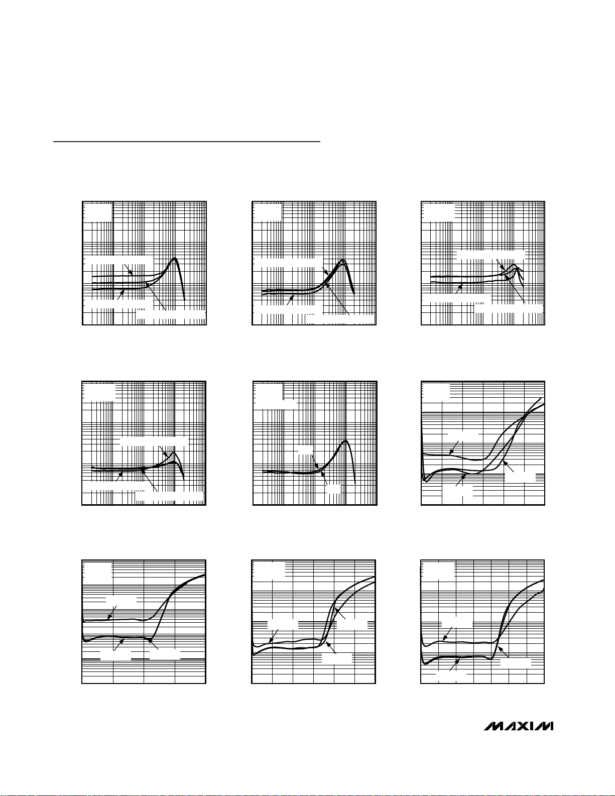
Typical Operating Characteristics
(VDD= PVDD= SHDN = 3.3V, GND = PGND = 0V, SYNC = VDD(SSM), gain = 6dB (GAIN1 = 0, GAIN2 = 1)).
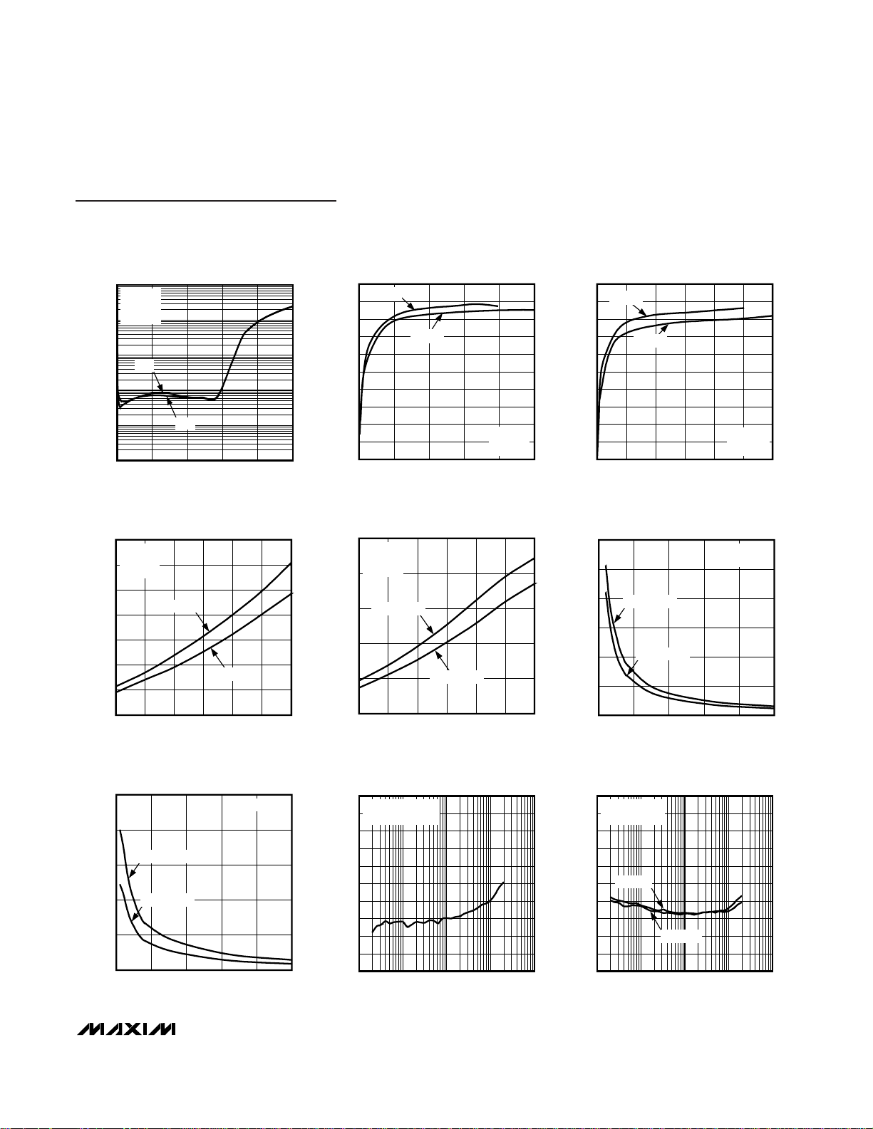
TOTAL HARMONIC DISTORTION
PLUS NOISE vs. FREQUENCY
MAX9701 toc01
FREQUENCY (Hz)
THD+N (%)
10k1k100
0.1
1
10
0.01
10 100k
VDD = 5V
R
L
= 4
Ω
OUTPUT POWER = 300mW
OUTPUT POWER = 100mW
OUTPUT POWER = 600mW
TOTAL HARMONIC DISTORTION
PLUS NOISE vs. FREQUENCY
MAX9701 toc02
FREQUENCY (Hz)
THD+N (%)
10k1k100
0.1
1
10
0.01
10 100k
VDD = 5V
R
L
= 8
Ω
OUTPUT POWER = 250mW
OUTPUT POWER = 100mW
OUTPUT POWER = 500mW
TOTAL HARMONIC DISTORTION
PLUS NOISE vs. FREQUENCY
MAX9701 toc03
FREQUENCY (Hz)
THD+N (%)
10k1k100
0.1
1
10
0.01
10 100k
VDD = 3.3V
R
L
= 4
Ω
OUTPUT POWER = 300mW
OUTPUT POWER = 100mW
OUTPUT POWER = 600mW
TOTAL HARMONIC DISTORTION
PLUS NOISE vs. FREQUENCY
MAX9701 toc04
FREQUENCY (Hz)
THD+N (%)
10k1k100
0.1
1
10
0.01
10 100k
VDD = 3.3V
R
L
= 8
Ω
OUTPUT POWER = 100mW
OUTPUT POWER = 400mW
OUTPUT POWER = 250mW
TOTAL HARMONIC DISTORTION
PLUS NOISE vs. FREQUENCY
MAX9701 toc05
FREQUENCY (Hz)
THD+N (%)
10k1k100
0.1
1
10
0.01
10 100k
VDD = 5V
R
L
= 8
Ω
P
OUT
= 800mW
FFM
SSM
TOTAL HARMONIC DISTORTION
PLUS NOISE vs. OUTPUT POWER
MAX9701 toc06
OUTPUT POWER (W)
THD+N (%)
2.52.01.51.00.5
0.1
1
10
100
0.01
03.0
VDD = 5V
R
L
= 4Ω
fIN = 10kHz
fIN = 20kHz
fIN = 1kHz
TOTAL HARMONIC DISTORTION
PLUS NOISE vs. OUTPUT POWER
MAX9701 toc07
OUTPUT POWER (W)
THD+N (%)
1.51.00.5
0.01
0.1
1
10
100
0.001
02.0
VDD = 5V
R
L
= 8Ω
fIN = 10kHz
fIN = 20kHz
fIN = 1kHz
TOTAL HARMONIC DISTORTION
PLUS NOISE vs. OUTPUT POWER
MAX9701 toc08
OUTPUT POWER (W)
THD+N (%)
1.00.80.60.40.2
0.1
1
10
100
0.01
0 1.2
VDD = 3.3V
R
L
= 4Ω
fIN = 10kHz
fIN = 20kHz
fIN = 1kHz
TOTAL HARMONIC DISTORTION
PLUS NOISE vs. OUTPUT POWER
MAX9701 toc09
OUTPUT POWER (mW)
THD+N (%)
600500400300200100
0.1
1
10
100
0.01
0700
VDD = 3.3V
R
L
= 8Ω
fIN = 10kHz
fIN = 20kHz
fIN = 1kHz
MAX9701
1.3W, Filterless, Stereo Class D Audio
Power Amplifier
_______________________________________________________________________________________ 5
TOTAL HARMONIC DISTORTION
PLUS NOISE vs. OUTPUT POWER
MAX9701 toc10
OUTPUT POWER (W)
THD+N (%)
1.61.20.80.4
0.01
0.1
1
10
100
0.001
02.0
VDD = 5V
R
L
= 8Ω
f
IN
= 1kHz
SSM
FFM
EFFICIENCY vs. OUTPUT POWER
MAX9701 toc11
OUTPUT POWER (W)
EFFICIENCY (%)
2.01.51.00.5
10
20
30
40
50
60
70
80
90
100
0
02.5
RL = 8Ω
RL = 4Ω
VDD = 5V
f
IN
= 1kHz
EFFICIENCY vs. OUTPUT POWER
MAX9701 toc12
OUTPUT POWER (W)
EFFICIENCY (%)
1.00.80.60.40.2
10
20
30
40
50
60
70
80
90
100
0
01.2
RL = 8Ω
RL = 4Ω
VDD = 3.3V
f
IN
= 1kHz
OUTPUT POWER vs. SUPPLY VOLTAGE
MAX9701 toc13
SUPPLY VOLTAGE (V)
OUTPUT POWER (W)
5.04.54.03.53.0
0.5
1.0
1.5
2.0
2.5
3.0
3.5
0
2.5 5.5
RL = 4Ω
A
V
= 12dB
f
IN
= 1kHz
THD+N = 10%
THD+N = 1%
OUTPUT POWER vs. SUPPLY VOLTAGE
MAX9701 toc14
SUPPLY VOLTAGE (V)
OUTPUT POWER (W)
5.04.54.03.53.0
0.4
0.8
1.2
1.6
2.0
0
2.5 5.5
RL = 8Ω
A
V
= 12dB
f
IN
= 1kHz
THD+N = 10%
THD+N = 1%
OUTPUT POWER vs. LOAD RESISTANCE
MAX9701 toc15
LOAD RESISTANCE (Ω)
OUTPUT POWER (W)
80604020
0.5
1.0
1.5
2.0
2.5
3.0
0
0100
VDD = 5V
f
IN
= 1kHz
THD+N = 10%
THD+N = 1%
OUTPUT POWER vs. LOAD RESISTANCE
MAX9701 toc16
LOAD RESISTANCE (Ω)
OUTPUT POWER (W)
80604020
0.4
0.8
1.2
1.6
2.0
0
0 100
fIN = 1kHz
THD+N = 10%
THD+N = 1%
POWER-SUPPLY REJECTION RATIO
vs. FREQUENCY
MAX9701 toc17
FREQUENCY (Hz)
PSRR (dB)
10k1k100
-90
-80
-70
-60
-50
-40
-30
-20
-10
0
-100
10 100k
V
RIPPLE
= 100mV
P-P
RL = 8Ω
COMMON-MODE REJECTION RATIO
vs. FREQUENCY
MAX9701 toc18
FREQUENCY (Hz)
CMRR (dB)
10k1k100
-90
-80
-70
-60
-50
-40
-30
-20
-10
0
-100
10 100k
VCM = 100mV
P-P
RL = 8Ω
VDD = 5V
VDD = 3.3V
Typical Operating Characteristics (continued)
(VDD= PVDD= SHDN = 3.3V, GND = PGND = 0V, SYNC = VDD(SSM), gain = 6dB (GAIN1 = 0, GAIN2 = 1)).
MAX9701
1.3W, Filterless, Stereo Class D Audio
Power Amplifier
6 _______________________________________________________________________________________
Typical Operating Characteristics (continued)
(VDD= PVDD= SHDN = 3.3V, GND = PGND = 0V, SYNC = VDD(SSM), gain = 6dB (GAIN1 = 0, GAIN2 = 1)).
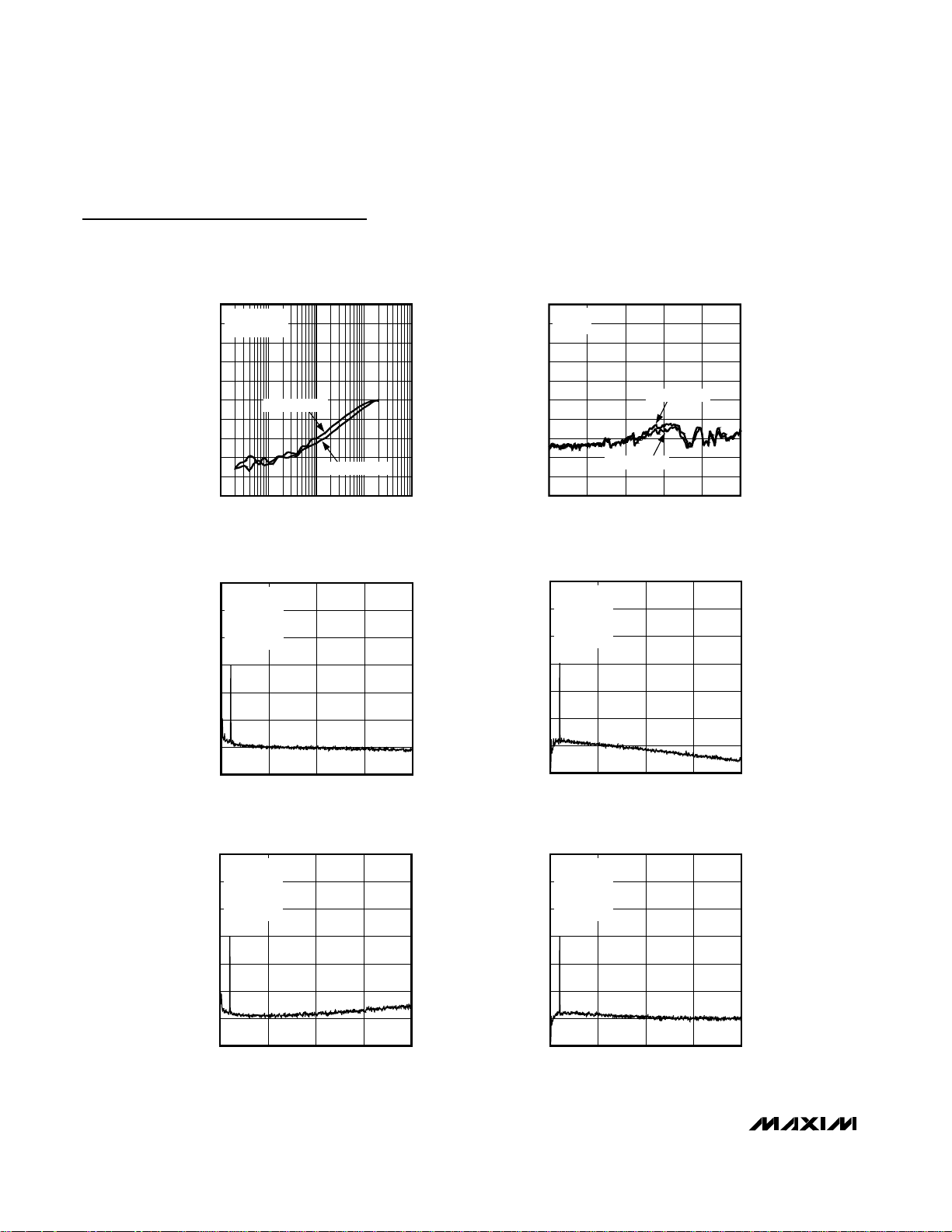
CROSSTALK vs. FREQUENCY
MAX9701 toc19
FREQUENCY (Hz)
CROSSTALK (dB)
10k1k100
-120
-110
-100
-90
-80
-70
-60
-50
-40
-30
-130
10 100k
RIGHT TO LEFT
LEFT TO RIGHT
P
OUT
= 300mW
R
L
= 8Ω
CROSSTALK vs. INPUT AMPLITUDE
MAX9701 toc20
INPUT AMPLITUDE (dB)
CROSSTALK (dB)
-14-34-54-74
-120
-110
-100
-90
-80
-70
-60
-50
-40
-30
-130
-94 6
RL = 8Ω
f
IN
= 1kHz
RIGHT TO LEFT
LEFT TO RIGHT
OUTPUT FREQUENCY SPECTRUM
MAX9701 toc21
FREQUENCY (Hz)
OUTPUT MAGNITUDE (dBV)
15k10k5k
-120
-100
-80
-60
-40
-20
0
-140
0 20k
FFM MODE
V
OUT
= -60dBV
f = 1kHz
R
L
= 8Ω
UNWEIGHTED
OUTPUT FREQUENCY SPECTRUM
MAX9701 toc22
FREQUENCY (Hz)
OUTPUT MAGNITUDE (dBV)
15k10k5k
-120
-100
-80
-60
-40
-20
0
-140
020k
FFM MODE
V
OUT
= -60dBV
f = 1kHz
R
L
= 8Ω
A-WEIGHTED
OUTPUT FREQUENCY SPECTRUM
MAX9701 toc23
FREQUENCY (Hz)
OUTPUT MAGNITUDE (dBV)
15k10k5k
-120
-100
-80
-60
-40
-20
0
-140
0 20k
SSM MODE
V
OUT
= -60dBV
f = 1kHz
R
L
= 8Ω
UNWEIGHTED
OUTPUT FREQUENCY SPECTRUM
MAX9701 toc24
FREQUENCY (Hz)
OUTPUT MAGNITUDE (dBV)
15k10k5k
-120
-100
-80
-60
-40
-20
0
-140
020k
SSM MODE
V
OUT
= -60dBV
f = 1kHz
R
L
= 8Ω
A-WEIGHTED

MAX9701
1.3W, Filterless, Stereo Class D Audio
Power Amplifier
_______________________________________________________________________________________ 7
WIDEBAND OUTPUT SPECTRUM
(FFM MODE)
MAX9701 toc25
FREQUENCY (Hz)
OUTPUT MAGNITUDE (dB)
100k10k
-90
-80
-70
-60
-50
-40
-30
-20
-10
0
-100
1k 1M
RBW = 10kHz
INPUT AC GROUNDED
WIDEBAND OUTPUT SPECTRUM
(SSM MODE)
MAX9701 toc26
FREQUENCY (Hz)
OUTPUT MAGNITUDE (dB)
100k10k
-90
-80
-70
-60
-50
-40
-30
-20
-10
0
-100
1k 1M
RBW = 10kHz
INPUT AC GROUNDED
TURN-ON/TURN-OFF RESPONSE
MAX9701 toc27
MAX9701
OUTPUT
SHDN
0V
250mV/div
2V/div
10ms/div
SUPPLY CURRENT
vs. SUPPLY VOLTAGE
MAX9701 toc28
SUPPLY VOLTAGE (V)
SUPPLY CURRENT (mA)
5.04.54.03.53.0
8
11
14
17
20
5
2.5 5.5
SSM
FFM
BOTH CHANNELS
SHUTDOWN CURRENT
vs. SUPPLY VOLTAGE
MAX9701 toc29
SUPPLY VOLTAGE (V)
SHUTDOWN CURRENT (µA)
5.04.54.03.53.0
1
2
3
4
5
0
2.5 5.5
BOTH CHANNELS
Typical Operating Characteristics (continued)
(VDD= PVDD= SHDN = 3.3V, GND = PGND = 0V, SYNC = VDD(SSM), gain = 6dB (GAIN1 = 0, GAIN2 = 1)).

MAX9701
1.3W, Filterless, Stereo Class D Audio
Power Amplifier
8 _______________________________________________________________________________________
Pin Description
PIN
TQFN UCSP
NAME FUNCTION
1A2SHDN Active-Low Shutdown. Connect to VDD for normal operation.
2 B3 SYNC
Frequency Select and External Clock Input.
SYNC = GND: Fixed-frequency mode with f
S
= 1100kHz.
SYNC = Unconnected: Fixed-frequency mode with f
S
= 1400kHz.
SYNC = V
DD
: Spread-spectrum mode with fS = 1200kHz ±60kHz.
SYNC = Clocked: Fixed-frequency mode with f
S
= external clock frequency.
3, 8, 11, 16
— N.C. No Connection. Not internally connected.
4 A3 OUTL+ Left-Channel Amplifier Output Positive Phase
5, 14 A4, D4 PV
DD
H-Bridge Power Supply. Connect to VDD. Bypass with a 0.1µF capacitor to PGND.
6, 13 B4, C4 PGND Power Ground
7 A5 OUTL- Left-Channel Amplifier Output Negative Phase
9, 22 B1, B5 GND Analog Ground
10 C5
Clock Signal Output
12 D5 OUTR- Right-Channel Amplifier Output Negative Phase
15 D3 OUTR+ Right-Channel Amplifier Output Positive Phase
17 C3 GAIN1 Gain-Select Input 1
18 D2 GAIN2 Gain-Select Input 2
19 D1 INR- Right-Channel Inverting Input
20 C2 INR+ Right-Channel Noninverting Input
21 C1 V
DD
Analog Power Supply. Connect to PVDD. Bypass with a 10µF capacitor to GND.
23 B2 INL+ Left-Channel Noninverting Input
24 A1 INL- Left-Channel Inverting Input
EP — EP
Exposed Pad. Connect the exposed thermal pad to the GND plane (see the Supply
Bypassing, Layout, and Grounding section).
SYNC_OUT

MAX9701
1.3W, Filterless, Stereo Class D Audio
Power Amplifier
_______________________________________________________________________________________ 9
Functional Diagram
V
BIAS
V
BIAS
CLASS D
MODULATOR
AND H-BRIDGE
CLASS D
MODULATOR
AND H-BRIDGE
BIAS
GENERATOR
OSCILLATOR
AND
SAWTOOTH
GAIN
CONTROL
OUTL+
V
BIAS
MAX9701
GND
PGND
OUTR+
OUTL-
OUTR-
SYNC_OUT
PV
DD
SYNC
INL+
INL-
INR+
INR-
GAIN1
GAIN2
SHDN
R
IN
R
IN
R
IN
R
IN
470nF
470nF
470nF
470nF
V
DD
V
DD
10µF 0.1µF
MAX9701
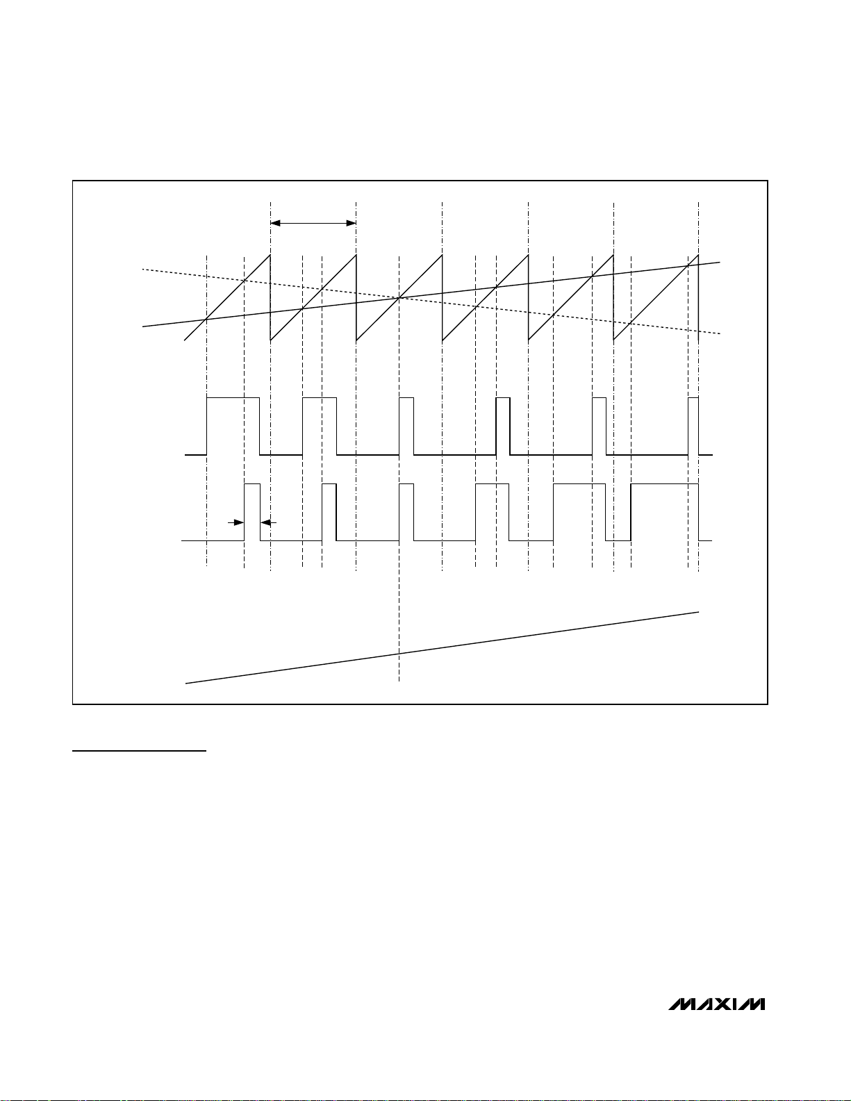
Detailed Description
The MAX9701 filterless, stereo Class D audio power
amplifier features several improvements to switch-mode
amplifier technology. The MAX9701 offers Class AB performance with Class D efficiency, while occupying minimal board space. A unique, filterless modulation
scheme, synchronizable switching frequency, and
spread-spectrum switching mode create a compact,
flexible, low-noise, efficient audio power amplifier. The
differential input architecture reduces common-mode
noise pickup, and can be used without input-coupling
capacitors. The inputs can also be configured to accept
a single-ended input signal.
Comparators monitor the MAX9701 inputs and compare
the complementary input voltages to the sawtooth waveform. The comparators trip when the input magnitude of
the sawtooth exceeds their corresponding input voltage.
Both comparators reset at a fixed time after the rising
edge of the second comparator trip point, generating a
minimum-width pulse (t
ON(MIN)
) at the output of the second comparator (Figure 1). As the input voltage increases
or decreases, the duration of the pulse at one output
increases while the other output pulse duration remains
the same. This causes the net voltage across the speaker
(V
OUT+
- V
OUT-
) to change. The minimum-width pulse
helps the device to achieve high levels of linearity.
1.3W, Filterless, Stereo Class D Audio
Power Amplifier
10 ______________________________________________________________________________________
OUT+
OUT-
V
IN-
V
IN+
V
OUT+
- V
OUT-
t
ON(MIN)
t
SW
Figure 1. MAX9701 Outputs with an Input Signal Applied

Operating Modes
Fixed-Frequency (FFM) Mode
The MAX9701 features two fixed-frequency modes.
Connect SYNC to GND to select a 1.1MHz switching frequency. Leave SYNC unconnected to select a 1.4MHz
switching frequency. The frequency spectrum of the
MAX9701 consists of the fundamental switching frequency and its associated harmonics (see the Wideband
Output Spectrum (FFM Mode) graph in the Typical
Operating Characteristics). Program the switching frequency so the harmonics do not fall within a sensitive frequency band (Table 1). Audio reproduction is not
affected by changing the switching frequency.
MAX9701
1.3W, Filterless, Stereo Class D Audio
Power Amplifier
______________________________________________________________________________________ 11
V
OUT_+
- V
OUT_-
t
SW
t
SW
t
SW
t
SW
V
IN_-
V
IN_+
OUT_+
OUT_-
t
ON(MIN)
Figure 2. MAX9701 Outputs with an Input Signal Applied (SSM Mode)
Table 1. Operating Modes
SYNC MODE
GND FFM with f
OSC
= 1100kHz
Unconnected FFM with f
OSC
= 1400kHz
V
DD
SSM with f
OSC
= 1200kHz ±60kHz
Clocked FFM with f
OSC
= external clock frequency
MAX9701
Spread-Spectrum (SSM) Mode
The MAX9701 features a unique, patented spreadspectrum mode that flattens the wideband spectral
components, improving EMI emissions that may be
radiated by the speaker and cables. This mode is
enabled by setting SYNC = V
DD
(Table 1). In SSM
mode, the switching frequency varies randomly by
±60kHz around the center frequency (1.2MHz). The
modulation scheme remains the same, but the period
of the sawtooth waveform changes from cycle to cycle
(Figure 2). Instead of a large amount of spectral energy
present at multiples of the switching frequency, the
energy is now spread over a bandwidth that increases
with frequency. Above a few megahertz, the wideband
spectrum looks like white noise for EMI purposes
(Figure 3). A proprietary amplifier topology ensures this
does not corrupt the noise floor in the audio bandwidth.
Synchronous Switching Mode
SYNC
The SYNC input allows the MAX9701 to be synchronized
to a user-defined clock, or another Maxim Class D amplifier, creating a fully synchronous system, minimizing
clock intermodulation, and allocating spectral components of the switching harmonics to insensitive frequency
bands. Applying a TTL clock signal between 1000kHz
and 1600kHz to SYNC synchronizes the MAX9701. The
period of the SYNC clock can be randomized, allowing
the MAX9701 to be synchronized to another Maxim Class
D amplifier operating in SSM mode.
SYNC_OUT
SYNC_OUT allows several MAX9701s as well as other
Class D amplifiers (such as the MAX9700) to be cascaded. The synchronized output minimizes interference due to clock intermodulation caused by the
switching spread between single devices. Using
SYNC_OUT, the modulation scheme remains the same
and audio reproduction is not affected by changing the
switching frequency.
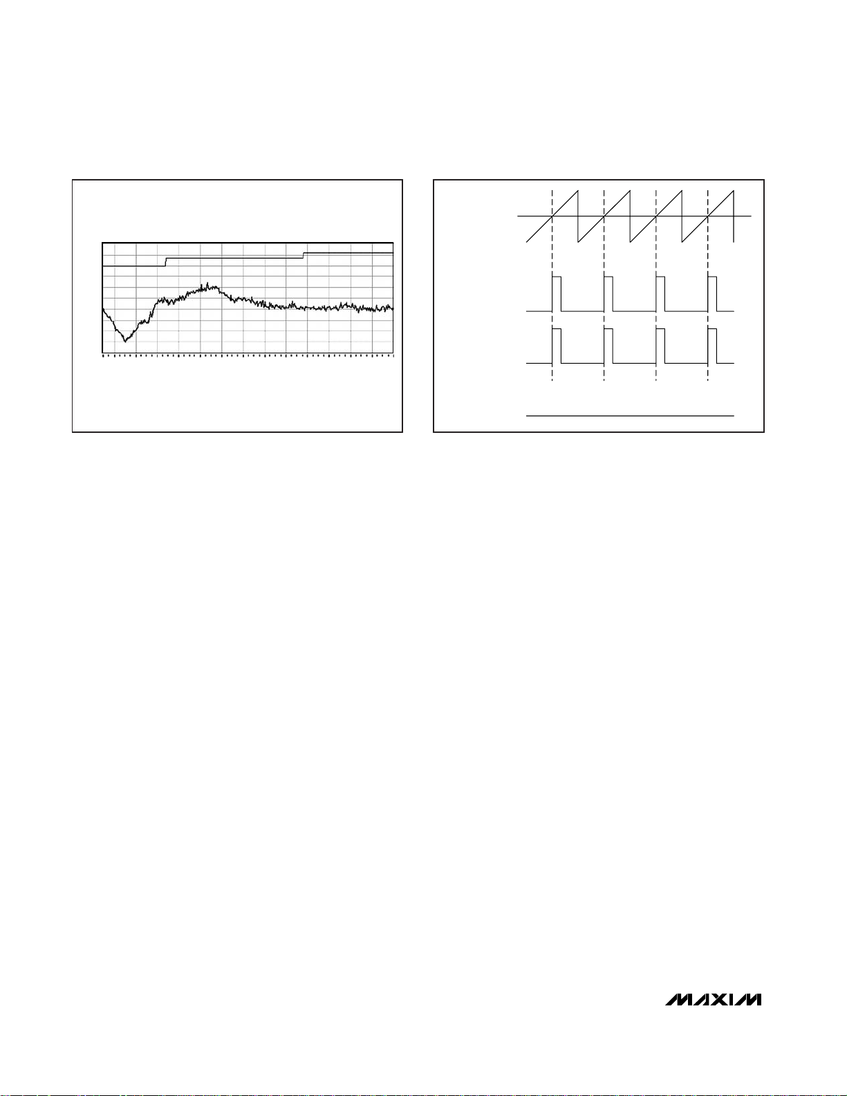
Filterless Modulation/Common-Mode Idle
The MAX9701 uses Maxim’s unique, patented modulation
scheme that eliminates the LC filter required by traditional
class D amplifiers, improving efficiency, reducing component count, conserving board space and system cost.
Conventional Class D amplifiers output a 50% duty cycle,
180° out-of-phase square wave when no signal is present. With no filter, the square wave appears across the
load as a DC voltage, resulting in finite load current,
which increases power consumption especially when
idling. When no signal is present at the input of the
MAX9701, the amplifiers will output an in-phase square
wave as shown in Figure 4. Because the MAX9701 drives
the speaker differentially, the two outputs cancel each
other, resulting in no net idle mode voltage across the
speaker, minimizing power consumption.
Efficiency
Efficiency of a Class D amplifier is due to the switching
operation of the output stage transistors. In a Class D
amplifier, the output transistors act as current-steering
switches and consume negligible additional power.
Any power loss associated with the Class D output
stage is mostly due to the I2R loss of the MOSFET onresistance, and quiescent-current overhead.
1.3W, Filterless, Stereo Class D Audio
Power Amplifier
12 ______________________________________________________________________________________
V
IN_
= 0V
OUT_-
OUT_+
V
OUT_+
- V
OUT_-
= 0V
Figure 4. MAX9701 Outputs with No Input Signal
FREQUENCY (MHz)
AMPLITUDE (dBµV/m)
280260240200 22080 100 120 140 160 18060
5.0
10.0
15.0
20.0
25.0
30.0
35.0
40.0
45.0
50.0
0.0
30 300
Figure 3. MAX9701 with 76mm of Speaker Cable with TDK
Common-Mode Choke: TDK ACM4532-801-20-X
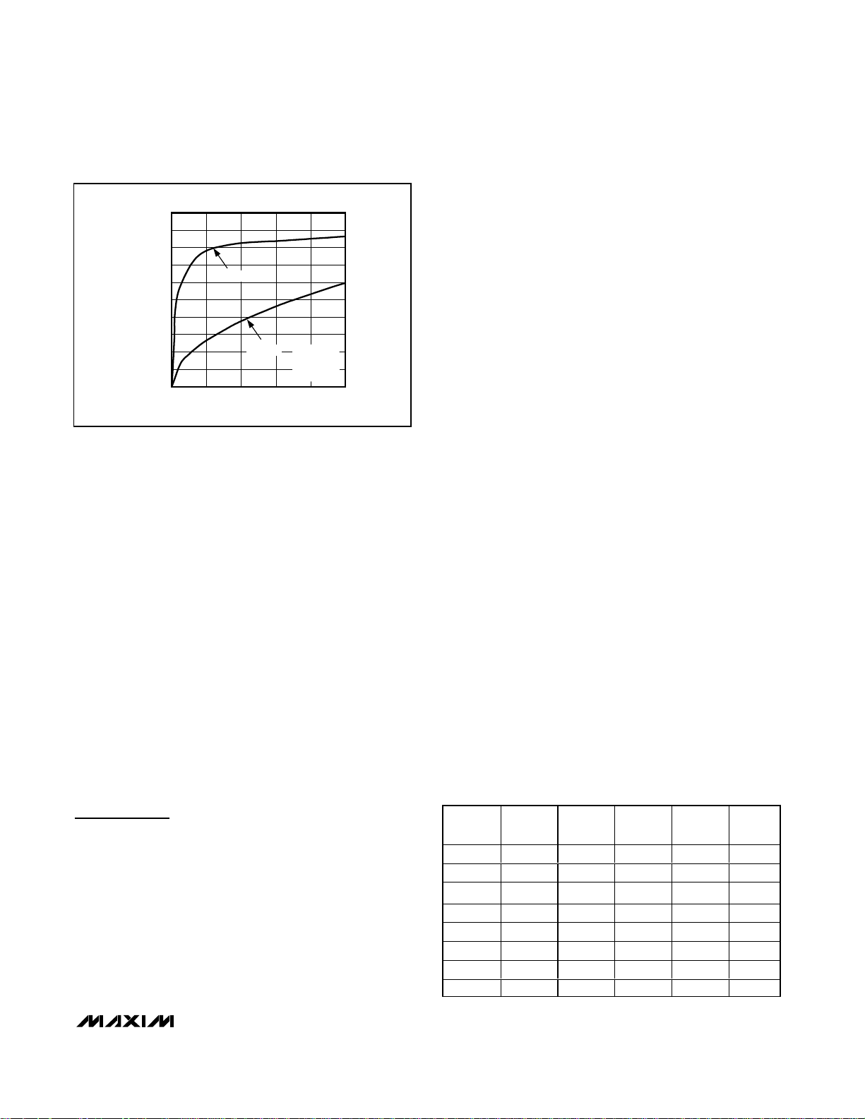
The theoretical best efficiency of a linear amplifier is
78%, however that efficiency is only exhibited at peak
output powers. Under normal operating levels (typical
music reproduction levels), efficiency falls below 30%,
whereas the MAX9701 still exhibits >80% efficiencies
under the same conditions (Figure 5).
Shutdown
The MAX9701 has a shutdown mode that reduces power
consumption and extends battery life. Driving SHDN low
places the MAX9701 in a low-power (0.1µA) shutdown
mode. Connect SHDN to V
DD
for normal operation.
Click-and-Pop Suppression
The MAX9701 features comprehensive click-and-pop
suppression that eliminates audible transients on startup
and shutdown. While in shutdown, the H-bridge is in a
high-impedance state. During startup, or power-up, the
input amplifiers are muted and an internal loop sets the
modulator bias voltages to the correct levels, preventing
clicks and pops when the H-bridge is subsequently
enabled. For 40ms following startup, a soft-start function
gradually unmutes the input amplifiers.
Applications Information
Filterless Operation
Traditional Class D amplifiers require an output filter to
recover the audio signal from the amplifier’s PWM output. The filters add cost, increase the solution size of
the amplifier, and can decrease efficiency. The traditional PWM scheme uses large differential output
swings (2 x V
DD(P-P)
) and causes large ripple currents.
Any parasitic resistance in the filter components results
in a loss of power, lowering the efficiency.
The MAX9701 does not require an output filter. The
device relies on the inherent inductance of the speaker
coil and the natural filtering of both the speaker and the
human ear to recover the audio component of the
square-wave output. Eliminating the output filter results
in a smaller, less costly, more efficient solution.
Because the frequency of the MAX9701 output is well
beyond the bandwidth of most speakers, voice coil
movement due to the square-wave frequency is very
small. Although this movement is small, a speaker not
designed to handle the additional power can be damaged. For optimum results, use a speaker with a series
inductance >10µH. Typical 8Ω speakers, for portable
audio applications, exhibit series inductances in the
range of 20µH to 100µH.
Output Offset
Unlike a Class AB amplifier, the output offset voltage of a
Class D amplifier does not noticeably increase quiescent
current draw when a load is applied. This is due to the
power conversion of the Class D amplifier. For example,
an 8mV DC offset across an 8Ω load results in 1mA extra
current consumption in a Class AB device. In the Class D
case, an 8mV offset into 8Ω equates to an additional
power drain of 8µW. Due to the high efficiency of the
Class D amplifier, this represents an additional quiescent
current draw of: 8µW/(V
DD
/ 100 x η), which is on the
order of a few µA.
Selectable Gain
The MAX9701 features four selectable gain settings,
minimizing external component count. Gains of 0dB,
3dB, 12dB, and 18dB are set through gain-select
inputs, GAIN1 and GAIN2. GAIN1 and GAIN2 can be
hard-wired or digitally controlled. Table 2 shows the
suggested gain settings to attain a maximum output
power from a given peak input voltage and given load
at VDD= 3.3V and THD+N = 10%.
MAX9701
1.3W, Filterless, Stereo Class D Audio
Power Amplifier
______________________________________________________________________________________ 13
0
30
20
10
50
40
90
80
70
60
100
0 0.1 0.2 0.40.3 0.5
EFFICIENCY vs. OUTPUT POWER
OUTPUT POWER (W)
EFFICIENCY (%)
MAX9701
CLASS AB
VDD = 3.3V
f = 1kHz
R
L
- 8Ω
Figure 5. MAX9701 Efficiency vs. Class AB Efficiency
GAIN1
GAIN
(dB)
INPUT
R
L
(Ω)
P
OUT
(mW)
0 0 +18
4
1100
1 0 +12
4
1100
01+6
4
1100
110
4
1100
0 0 +18
8
725
1 0 +12
8
725
01+6
8
725
110
8
725
Table 2. Gain Settings
GAIN2
(V
RMS
0.305
0.615
1.213
2.105
0.345
0.686
1.360
2.705
)

MAX9701
Input Amplifier
Differential Input
The MAX9701 features a differential input structure,
making it compatible with many CODECs and offers
improved noise immunity over a single-ended input
amplifier. In devices such as cellular phones, high-frequency signals from the RF transmitter can be picked
up by the amplifier’s input traces. The signals appear at
the amplifier’s inputs as common-mode noise. A differential input amplifier amplifies the difference of the two
inputs, any signal common to both inputs is canceled.
Single-Ended Input
The MAX9701 can be configured as a single-ended
input amplifier by capacitively coupling either input to
GND, and driving the other input (Figure 6).
DC-Coupled Inputs
The input amplifier can accept DC-coupled inputs that
are biased within the amplifier’s common-mode range
(see the Typical Operating Characteristics). DC coupling eliminates the input-coupling capacitors, reducing component count to potentially two external
components (Figure 7). However, the highpass filtering
effect of the capacitors is lost, allowing low-frequency
signals to feed through to the load.
Component Selection
Input Filter
An input capacitor, CIN, in conjunction with the
MAX9701 input impedance (RIN) forms a highpass filter
that removes the DC bias from an incoming signal. The
AC-coupling capacitor allows the amplifier to automatically bias the signal to an optimum DC level. Assuming
zero-source impedance, the -3dB point of the highpass
filter is given by:
Choose CINso f
-3dB
is well below the lowest frequency of
interest. Use capacitors whose dielectrics have low-voltage coefficients, such as tantalum or aluminum electrolytic. Capacitors with high-voltage coefficients, such as
ceramics, may result in increased distortion at low frequencies.
Other considerations when designing the input filter
include the constraints of the overall system and the
actual frequency band of interest. Although high-fidelity
audio calls for a flat-gain response between 20Hz and
20kHz, portable voice-reproduction devices such as
cellular phones and two-way radios need only concentrate on the frequency range of the spoken human voice
(typically 300Hz to 3.5kHz). In addition, speakers used
f
RC
dB
IN IN
−=3
1
2π
1.3W, Filterless, Stereo Class D Audio
Power Amplifier
14 ______________________________________________________________________________________
MAX9701
0.1µF10µF
2.5V TO 5.5V
0.47µF
0.47µF
0.47µF
0.47µF
SINGLE-ENDED
LEFT AUDIO INPUT
SINGLE-ENDED
RIGHT AUDIO INPUT
OUTL+
OUTL-
OUTR+
OUTR-
GAIN1
GND
PGND
SYNC
INL+
INR+
INL-
INR-
GAIN2
SHDN
V
DD
PV
DD
FFM MODE WITH f
OSC
= 1100kHz, GAIN = 6dB.
Figure 6. Single-Ended Input
MAX9701
0.1µF10µF
2.5V TO 5.5V
OUTL+
OUTL-
OUTR+
OUTR-
GAIN1
GND
PGND
SYNC
INL+
INR+
INL-
INR-
GAIN2
SHDN
V
DD
PV
DD
FFM MODE WITH f
OSC
= 1100kHz, GAIN = 6dB
CODEC BIASED TO 1/2 MAX9701 COMMON-MODE VOLTAGE.
CODEC
Figure 7. DC-Coupled Inputs

in portable devices typically have a poor response
below 300Hz. Taking these two factors into consideration, the input filter may not need to be designed for a
20Hz to 20kHz response, saving both board space and
cost due to the use of smaller capacitors.
Output Filter
The MAX9701 does not require an output filter. The
device passes FCC emissions standards with 76mm of
unshielded speaker cables. However, output filtering
can be used if a design is failing radiated emissions due
to board layout or cable length, or if the circuit is near
EMI-sensitive devices. Use a ferrite bead filter when
radiated frequencies above 10MHz are of concern. Use
an LC filter or a common-mode choke when radiated
emissions below 10MHz are of concern, or when long
leads (>76mm) connect the amplifier to the speaker.
2.1 Channel Configuration
The typical 2.1 channel application circuit (Figure 8)
shows the MAX9701 configured as a mid-/high-frequency
amplifier and the MAX9700 configured as a mono bass
amplifier. Input capacitors (C
IN
) set the highpass cutoff
frequency according to the following equation:
where RINis the typical input resistance of the
MAX9701. The 10µF capacitors on the output of the
MAX9701 ensure a two-pole highpass filter.
f
RC
IN IN
=
××
1
2π
MAX9701
1.3W, Filterless, Stereo Class D Audio
Power Amplifier
______________________________________________________________________________________ 15
MAX9701
MAX9700
MAX4238
INR+
INL+
INL-
INR-
SYNC
5V
OUTL+
OUTL-
OUTR+
OUTR-
8Ω
8Ω
SYNC_OUT
10µF
10µF
C
IN
2200pF
1µF
1µF
5V
NOTE: VALUES SHOWN ARE FOR A LOWPASS CUTOFF OF 2Hz AND A BASS GAIN OF -1V/V.
FFM MODE WITH f
OSC
= 1100kHz.
OUT+
OUT-
SYNC
IN+
IN-
1.25V
R3
10kΩ
C2
1nF
R1
20kΩ
R2
20kΩ
R4
39kΩ
C2
0.01µF
V
DD
C
IN
2200pF
C
IN
2200pF
C
IN
2200pF
4Ω
Figure 8. 2.1 Channel Application Circuit

MAX9701
Low frequencies are summed through a two-pole lowpass filter and sent to the MAX9700 mono speaker
amplifier. The passband gain of the lowpass filter is
unity for in-phase stereo signals,
where R1 = R2 and R3 = R1//R2. The cutoff frequency
of the lowpass filter is set by the following equation:
Supply Bypassing, Layout, and Grounding
Proper layout and grounding are essential for optimum
performance. Use large traces for the power-supply
inputs and amplifier outputs to minimize losses due to
parasitic trace resistance. Large traces also aid in moving
heat away from the package. Proper grounding improves
audio performance, minimizes crosstalk between channels, and prevents any switching noise from coupling into
the audio signal. Connect PGND and GND together at a
single point on the PC board. Route all traces that carry
switching transients away from GND and the traces/components in the audio signal path.
Bypass VDDwith 10µF to GND and PVDDwith 0.1µF to
PGND. Place the bypass capacitors as close to the
MAX9701 as possible. Use large, low-resistance output
traces. Current drawn from the outputs increases as load
impedance decreases. High-output trace resistance
decreases the power delivered to the load. Large output,
supply, and GND traces allow more heat to move from
the MAX9701 to the air, decreasing the thermal impedance of the circuit.
The MAX9701 thin QFN-EP package features an
exposed thermal pad on its underside. This pad lowers
the package’s thermal impedance by providing a
direct heat conduction path from the die to the printed
circuit board. Connect the exposed thermal pad to the
GND plane.
UCSP Applications Information
For the latest application details on UCSP construction,
dimensions, tape carrier information, printed circuit board
techniques, bump-pad layout, and recommended reflow
temperature profile as well as the latest information on
reliability testing results, refer to Application Note:
UCSP—A Wafer-Level Chip-Scale Package available on
Maxim’s website at www.maxim-ic.com/ucsp.
f
CC R R
=×
×××
1
2
1
12 34π
− ×2
3
1
R
R
1.3W, Filterless, Stereo Class D Audio
Power Amplifier
16 ______________________________________________________________________________________

MAX9701
1.3W, Filterless, Stereo Class D Audio
Power Amplifier
______________________________________________________________________________________ 17
MAX4060
MAX9701
MAX9722B
CODEC
AUX_IN
BIAS
IN+
IN-
V
CC
OUTL-
OUTL+
OUTR+
OUTR-
INL
INR
C1P CIN
SV
SS
PV
SS
OUTR
OUTL
V
DD
0.1µF
0.1µF
0.1µF
2.2kΩ
2.2kΩ
V
DD
µCONTROLLER
INL+
SYNC
OUT
1µF
1µF
1µF
1µF
1µF
SHDN
SHDN
GND
470nF
470nF
470nF
470nF
GAIN1
GAIN2
INL-
INR-
INR+
0.1µF10µF
V
DD
V
DD
PV
DD
GND PGND
0.1µF
System Diagram
MAX9701
1.3W, Filterless, Stereo Class D Audio
Power Amplifier
18 ______________________________________________________________________________________
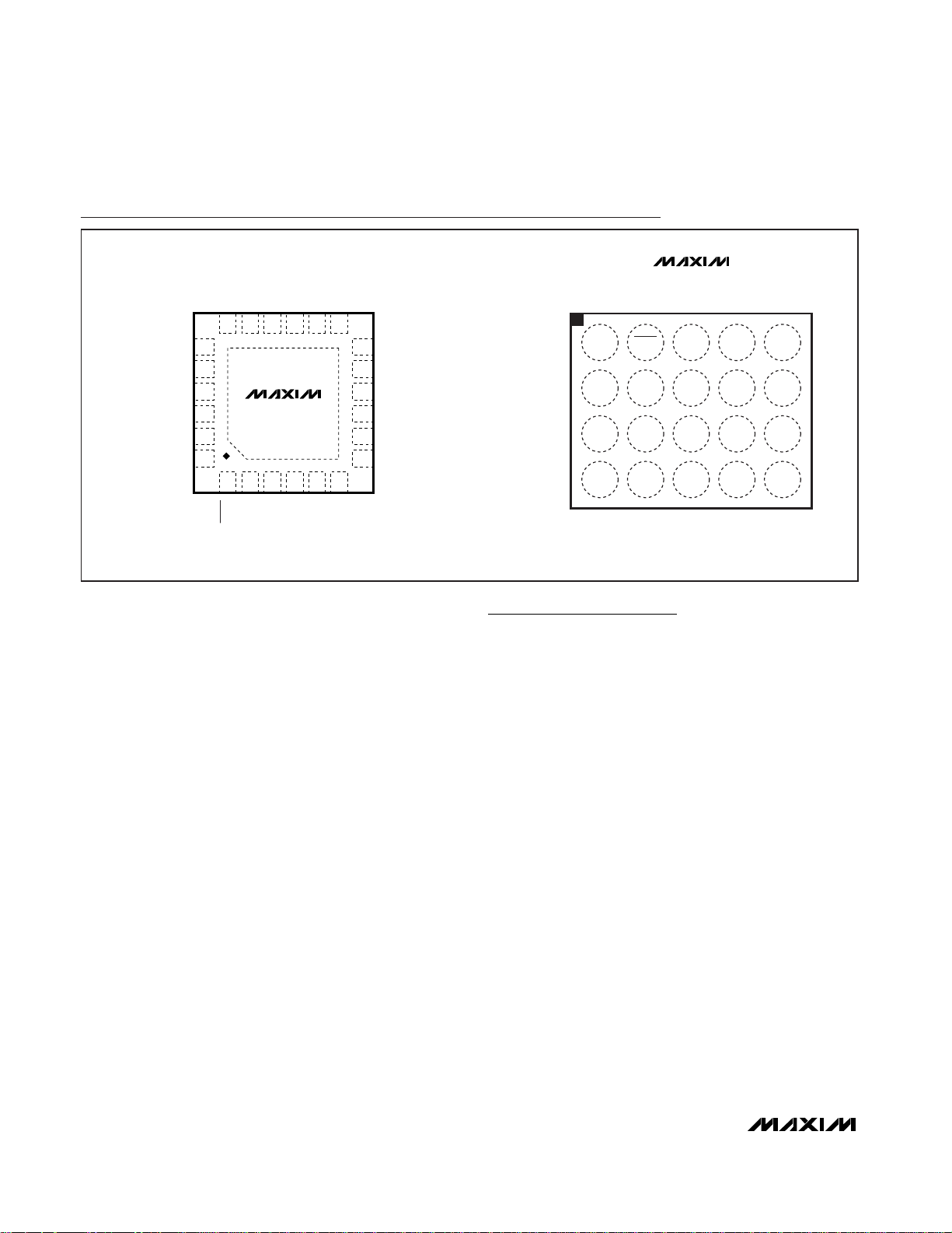
Chip Information
TRANSISTOR COUNT: 5688
PROCESS: BiCMOS
GND INL+ SYNC PGND GND
V
DD
INR+ GAIN1 PGND
SYNC
_OUT
INR- GAIN2 OUTR+ PV
DD
OUTR-
INL- SHDN OUTL+ PV
DD
OUTL-A
B
C
D
12345
MAX9701
UCSP
TOP VIEW
(BUMPS ON BOTTOM)
MAX9701
18 17 16 15 14
19
TQFN
TOP VIEW
13
1 2 3 4 5 6
24
23
22
21
20
12
7
8
9
10
11
INL+
V
DD
INR+
INR-
INL-
GND
N.C.
SYNC_OUT
N.C.
OUTR-
OUTL-
GND
SHDN
SYNC
N.C.
OUTL+
PV
DD
PGND
GAIN2
GAIN1
N.C.
OUTR+
PV
DD
PGND
Pin Configurations
MAX9701
1.3W, Filterless, Stereo Class D Audio
Power Amplifier
______________________________________________________________________________________ 19
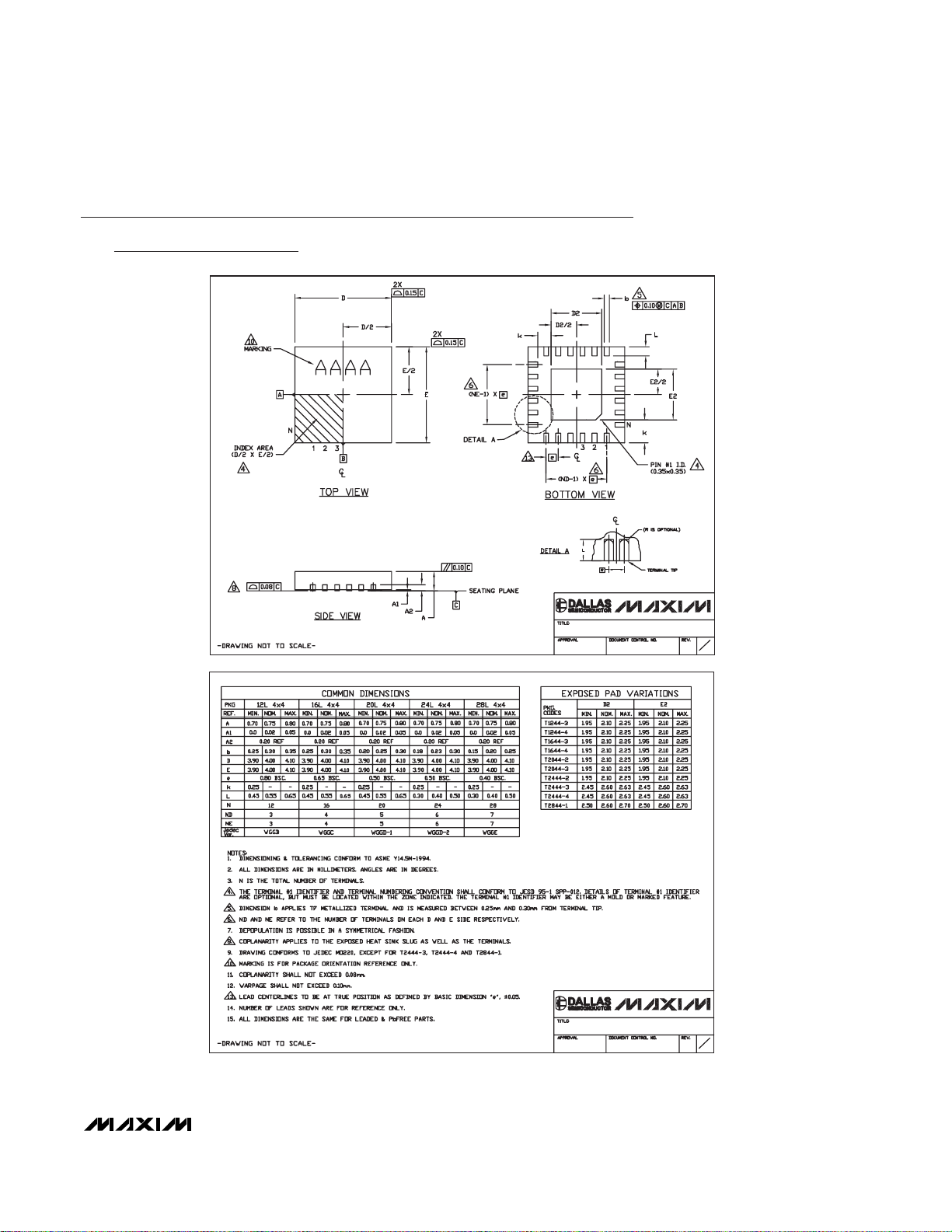
24L QFN THIN.EPS
PACKAGE OUTLINE,
21-0139
2
1
F
12, 16, 20, 24, 28L THIN QFN, 4x4x0.8mm
PACKAGE OUTLINE,
21-0139
2
2
F
12, 16, 20, 24, 28L THIN QFN, 4x4x0.8mm
Package Information
(The package drawing(s) in this data sheet may not reflect the most current specifications. For the latest package outline information,
go to www.maxim-ic.com/packages
.)
MAX9701 Package Code: T2444-4

MAX9701
1.3W, Filterless, Stereo Class D Audio
Power Amplifier
Maxim cannot assume responsibility for use of any circuitry other than circuitry entirely embodied in a Maxim product. No circuit patent licenses are
implied. Maxim reserves the right to change the circuitry and specifications without notice at any time.
20 ____________________Maxim Integrated Products, 120 San Gabriel Drive, Sunnyvale, CA 94086 408-737-7600
© 2007 Maxim Integrated Products is a registered trademark of Maxim Integrated Products, Inc.
Package Information (continued)
(The package drawing(s) in this data sheet may not reflect the most current specifications. For the latest package outline information,
go to www.maxim-ic.com/packages
.)
MAX9701 Package Code: B20-1
Revision History
Pages changed at Rev 2: 1, 5, 20
5x4 UCSP.EPS
 Loading...