

Page 1
19-5111; Rev 1; 7/10
EVALUATION KIT
AVAILABLE
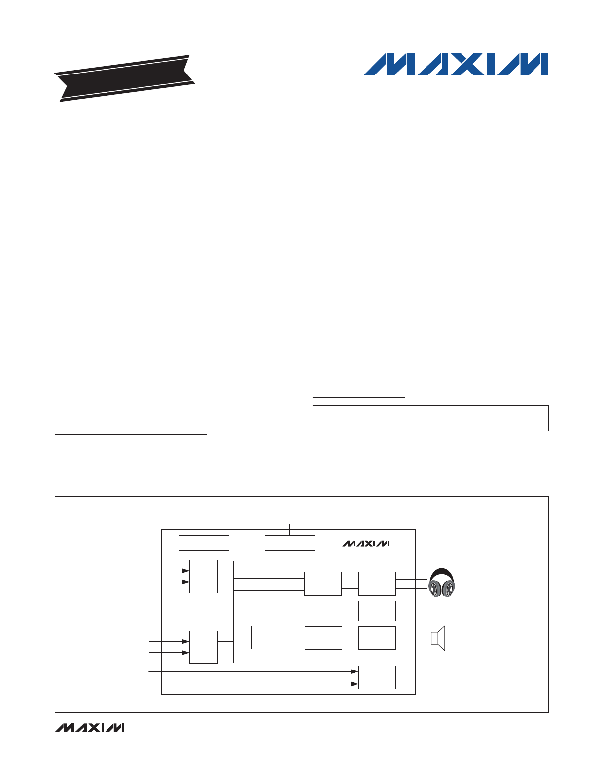
Audio Subsystem with Mono Class D
Speaker and Class H Headphone Amplifiers
General Description
The MAX97002 mono audio subsystem combines a
mono speaker amplifier with a stereo headphone amplifier and an analog DPST switch. The headphone and
speaker amplifiers have independent volume control and
on/off control. The 4 inputs are configurable as 2 differential inputs or 4 single-ended inputs.
The entire subsystem is designed for maximum efficiency. The high-efficiency, 700mW, Class D speaker
amplifier operates directly from the battery and consumes no more than 1FA in shutdown mode. The Class
H headphone amplifier utilizes a dual-mode charge
pump to maximize efficiency while outputting a groundreferenced signal that does not require output coupling
capacitors.
The speaker amplifier incorporates a distortion limiter to
automatically reduce the volume level when excessive
clipping occurs. This allows high gain for low-level signals without compromising the quality of large signals.
2
All control is performed using the 2-wire I
The MAX97002 operates over the extended -40NC to
+85NC temperature range, and is available in the 2mm x
2.5mm, 20-bump, WLP package (0.5mm pitch).
Applications
Cell Phones
Portable Media Players
C interface.
Features
S 2.7V to 5.5V Speaker Supply Voltage
S
1.6V to 2V Headphone Supply Voltage
S
700mW Speaker Output (V
= 8ω + 68µH)
Z
SPK
S
37mW/Channel Headphone Output (R
S
Low-Emission Class D Amplifier
S
Efficient Class H Headphone Amplifier
S
Ground-Referenced Headphone Outputs
S
2 Stereo Single-Ended/Mono Differential Inputs
S
Integrated Distortion Limiter (Speaker Outputs)
S
Integrated DPST Analog Switch
S
No Clicks and Pops
S
TDMA Noise Free
S
2mm x 2.5mm, 20-Bump, 0.5mm Pitch WLP
PVDD
= 3.7V,
HP
= 16I)
Package
Ordering Information
PART TEMP RANGE PIN-PACKAGE
MAX97002EWP+
-40NC to +85NC
20 WLP
MAX97002
Simplified Block Diagram
BATTERY1.8V
POWER SUPPLY
STEREO/
MONO
INPUT
STEREO/
MONO
INPUT
_______________________________________________________________ Maxim Integrated Products 1
For pricing, delivery, and ordering information, please contact Maxim Direct at 1-888-629-4642,
or visit Maxim’s website at www.maxim-ic.com.
LIMITER
I2C
CONTROL
VOLUME
VOLUME
MAX97002
CLASS H
AMPLIFIER
CHARGE
PUMP
CLASS D
AMPLIFIER
BYPASS
Page 2

Audio Subsystem with Mono Class D
Speaker and Class H Headphone Amplifiers
Table of ConTenTs
General Description . . . . . . . . . . . . . . . . . . . . . . . . . . . . . . . . . . . . . . . . . . . . . . . . . . . . . . . . . . . . . . . . . . . . . . . . . . . . 1
Applications . . . . . . . . . . . . . . . . . . . . . . . . . . . . . . . . . . . . . . . . . . . . . . . . . . . . . . . . . . . . . . . . . . . . . . . . . . . . . . . . . . 1
Features . . . . . . . . . . . . . . . . . . . . . . . . . . . . . . . . . . . . . . . . . . . . . . . . . . . . . . . . . . . . . . . . . . . . . . . . . . . . . . . . . . . . . 1
Simplified Block Diagram . . . . . . . . . . . . . . . . . . . . . . . . . . . . . . . . . . . . . . . . . . . . . . . . . . . . . . . . . . . . . . . . . . . . . . . . 1
Ordering Information . . . . . . . . . . . . . . . . . . . . . . . . . . . . . . . . . . . . . . . . . . . . . . . . . . . . . . . . . . . . . . . . . . . . . . . . . . . 1
Functional Diagram/Typical Application Circuit . . . . . . . . . . . . . . . . . . . . . . . . . . . . . . . . . . . . . . . . . . . . . . . . . . . . . . . 4
MAX97002
Absolute Maximum Ratings . . . . . . . . . . . . . . . . . . . . . . . . . . . . . . . . . . . . . . . . . . . . . . . . . . . . . . . . . . . . . . . . . . . . . . 5
Electrical Characteristics . . . . . . . . . . . . . . . . . . . . . . . . . . . . . . . . . . . . . . . . . . . . . . . . . . . . . . . . . . . . . . . . . . . . . . . . 5
Digital I/O Characteristics. . . . . . . . . . . . . . . . . . . . . . . . . . . . . . . . . . . . . . . . . . . . . . . . . . . . . . . . . . . . . . . . . . . . . . . . 9
2
C TIMING Characteristics . . . . . . . . . . . . . . . . . . . . . . . . . . . . . . . . . . . . . . . . . . . . . . . . . . . . . . . . . . . . . . . . . . . . . 10
I
Pin Configuration . . . . . . . . . . . . . . . . . . . . . . . . . . . . . . . . . . . . . . . . . . . . . . . . . . . . . . . . . . . . . . . . . . . . . . . . . . . . . 17
Pin Description . . . . . . . . . . . . . . . . . . . . . . . . . . . . . . . . . . . . . . . . . . . . . . . . . . . . . . . . . . . . . . . . . . . . . . . . . . . . . . . 17
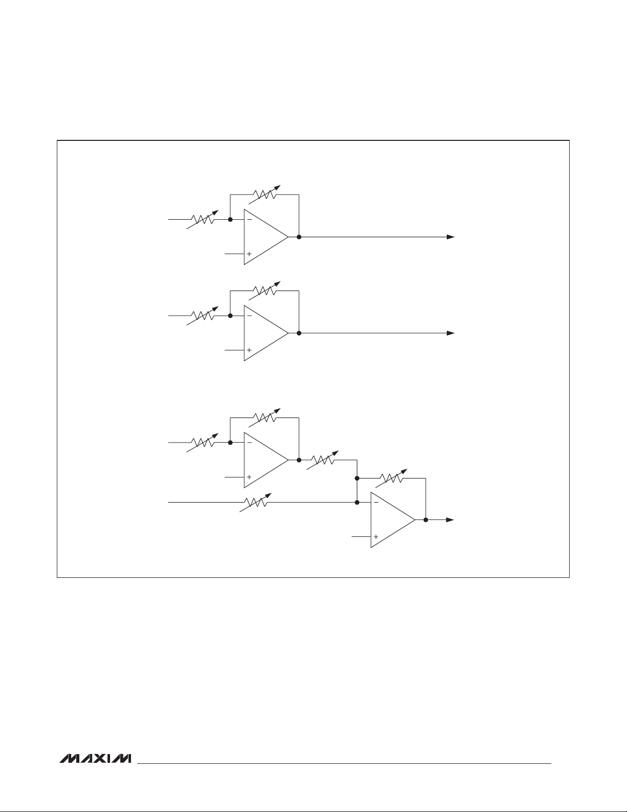
Detailed Description . . . . . . . . . . . . . . . . . . . . . . . . . . . . . . . . . . . . . . . . . . . . . . . . . . . . . . . . . . . . . . . . . . . . . . . . . . . 18
Signal Path . . . . . . . . . . . . . . . . . . . . . . . . . . . . . . . . . . . . . . . . . . . . . . . . . . . . . . . . . . . . . . . . . . . . . . . . . . . . . . . . 18
Mixers . . . . . . . . . . . . . . . . . . . . . . . . . . . . . . . . . . . . . . . . . . . . . . . . . . . . . . . . . . . . . . . . . . . . . . . . . . . . . . . . . . . . 18
Class D Speaker Amplifier . . . . . . . . . . . . . . . . . . . . . . . . . . . . . . . . . . . . . . . . . . . . . . . . . . . . . . . . . . . . . . . . . . . . 18
Ultra-Low EMI Filterless Output Stage . . . . . . . . . . . . . . . . . . . . . . . . . . . . . . . . . . . . . . . . . . . . . . . . . . . . . . . . .20
Distortion Limiter . . . . . . . . . . . . . . . . . . . . . . . . . . . . . . . . . . . . . . . . . . . . . . . . . . . . . . . . . . . . . . . . . . . . . . . . . 21
Analog Switch . . . . . . . . . . . . . . . . . . . . . . . . . . . . . . . . . . . . . . . . . . . . . . . . . . . . . . . . . . . . . . . . . . . . . . . . . . . . . . 21
Headphone Amplifier . . . . . . . . . . . . . . . . . . . . . . . . . . . . . . . . . . . . . . . . . . . . . . . . . . . . . . . . . . . . . . . . . . . . . . . . 21
DirectDrive . . . . . . . . . . . . . . . . . . . . . . . . . . . . . . . . . . . . . . . . . . . . . . . . . . . . . . . . . . . . . . . . . . . . . . . . . . . . . . 21
Charge Pump . . . . . . . . . . . . . . . . . . . . . . . . . . . . . . . . . . . . . . . . . . . . . . . . . . . . . . . . . . . . . . . . . . . . . . . . . . . . 22
Class H Operation . . . . . . . . . . . . . . . . . . . . . . . . . . . . . . . . . . . . . . . . . . . . . . . . . . . . . . . . . . . . . . . . . . . . . . . . 22
Low-Power Mode . . . . . . . . . . . . . . . . . . . . . . . . . . . . . . . . . . . . . . . . . . . . . . . . . . . . . . . . . . . . . . . . . . . . . . . . . 22
2
C Slave Address. . . . . . . . . . . . . . . . . . . . . . . . . . . . . . . . . . . . . . . . . . . . . . . . . . . . . . . . . . . . . . . . . . . . . . . . . . . 22
I
2
C Registers . . . . . . . . . . . . . . . . . . . . . . . . . . . . . . . . . . . . . . . . . . . . . . . . . . . . . . . . . . . . . . . . . . . . . . . . . . . . 23
I
Mixers . . . . . . . . . . . . . . . . . . . . . . . . . . . . . . . . . . . . . . . . . . . . . . . . . . . . . . . . . . . . . . . . . . . . . . . . . . . . . . . . . . . . 25
Volume Control . . . . . . . . . . . . . . . . . . . . . . . . . . . . . . . . . . . . . . . . . . . . . . . . . . . . . . . . . . . . . . . . . . . . . . . . . . . . . 26
Distortion Limiter . . . . . . . . . . . . . . . . . . . . . . . . . . . . . . . . . . . . . . . . . . . . . . . . . . . . . . . . . . . . . . . . . . . . . . . . . . . . 29
Power Management . . . . . . . . . . . . . . . . . . . . . . . . . . . . . . . . . . . . . . . . . . . . . . . . . . . . . . . . . . . . . . . . . . . . . . . . .29
Charge-Pump Control. . . . . . . . . . . . . . . . . . . . . . . . . . . . . . . . . . . . . . . . . . . . . . . . . . . . . . . . . . . . . . . . . . . . . . . . 30
2
C Serial Interface . . . . . . . . . . . . . . . . . . . . . . . . . . . . . . . . . . . . . . . . . . . . . . . . . . . . . . . . . . . . . . . . . . . . . . . . . . 30
I
Bit Transfer . . . . . . . . . . . . . . . . . . . . . . . . . . . . . . . . . . . . . . . . . . . . . . . . . . . . . . . . . . . . . . . . . . . . . . . . . . . . . .30
START and STOP Conditions. . . . . . . . . . . . . . . . . . . . . . . . . . . . . . . . . . . . . . . . . . . . . . . . . . . . . . . . . . . . . . . .30
Charge-Pump Control. . . . . . . . . . . . . . . . . . . . . . . . . . . . . . . . . . . . . . . . . . . . . . . . . . . . . . . . . . . . . . . . . . . . . . . . 30
2
Page 3

Audio Subsystem with Mono Class D
Speaker and Class H Headphone Amplifiers
Table of ConTenTs (ConTinued)
Early STOP Conditions. . . . . . . . . . . . . . . . . . . . . . . . . . . . . . . . . . . . . . . . . . . . . . . . . . . . . . . . . . . . . . . . . . . . . 31
Slave Address . . . . . . . . . . . . . . . . . . . . . . . . . . . . . . . . . . . . . . . . . . . . . . . . . . . . . . . . . . . . . . . . . . . . . . . . . . . 31
Acknowledge . . . . . . . . . . . . . . . . . . . . . . . . . . . . . . . . . . . . . . . . . . . . . . . . . . . . . . . . . . . . . . . . . . . . . . . . . . . . 31
Write Data Format . . . . . . . . . . . . . . . . . . . . . . . . . . . . . . . . . . . . . . . . . . . . . . . . . . . . . . . . . . . . . . . . . . . . . . . . 31
Read Data Format . . . . . . . . . . . . . . . . . . . . . . . . . . . . . . . . . . . . . . . . . . . . . . . . . . . . . . . . . . . . . . . . . . . . . . . . 32
Applications Information. . . . . . . . . . . . . . . . . . . . . . . . . . . . . . . . . . . . . . . . . . . . . . . . . . . . . . . . . . . . . . . . . . . . . . . . 33
Filterless Class D Operation . . . . . . . . . . . . . . . . . . . . . . . . . . . . . . . . . . . . . . . . . . . . . . . . . . . . . . . . . . . . . . . . . . .33
RF Susceptibility . . . . . . . . . . . . . . . . . . . . . . . . . . . . . . . . . . . . . . . . . . . . . . . . . . . . . . . . . . . . . . . . . . . . . . . . . . . .33
Component Selection . . . . . . . . . . . . . . . . . . . . . . . . . . . . . . . . . . . . . . . . . . . . . . . . . . . . . . . . . . . . . . . . . . . . . . . . 34
Optional Ferrite Bead Filter . . . . . . . . . . . . . . . . . . . . . . . . . . . . . . . . . . . . . . . . . . . . . . . . . . . . . . . . . . . . . . . . . 34
Input Capacitor. . . . . . . . . . . . . . . . . . . . . . . . . . . . . . . . . . . . . . . . . . . . . . . . . . . . . . . . . . . . . . . . . . . . . . . . . . . 34
Charge-Pump Capacitor Selection . . . . . . . . . . . . . . . . . . . . . . . . . . . . . . . . . . . . . . . . . . . . . . . . . . . . . . . . . . . 34
Charge-Pump Flying Capacitor . . . . . . . . . . . . . . . . . . . . . . . . . . . . . . . . . . . . . . . . . . . . . . . . . . . . . . . . . . . . . . 34
Charge-Pump Holding Capacitor . . . . . . . . . . . . . . . . . . . . . . . . . . . . . . . . . . . . . . . . . . . . . . . . . . . . . . . . . . . . 34
Supply Bypassing, Layout, and Grounding . . . . . . . . . . . . . . . . . . . . . . . . . . . . . . . . . . . . . . . . . . . . . . . . . . . . . 34
WLP Applications Information . . . . . . . . . . . . . . . . . . . . . . . . . . . . . . . . . . . . . . . . . . . . . . . . . . . . . . . . . . . . . . . 35
Package Information. . . . . . . . . . . . . . . . . . . . . . . . . . . . . . . . . . . . . . . . . . . . . . . . . . . . . . . . . . . . . . . . . . . . . . . . . . . 36
MAX97002
3
Page 4
Audio Subsystem with Mono Class D
Speaker and Class H Headphone Amplifiers
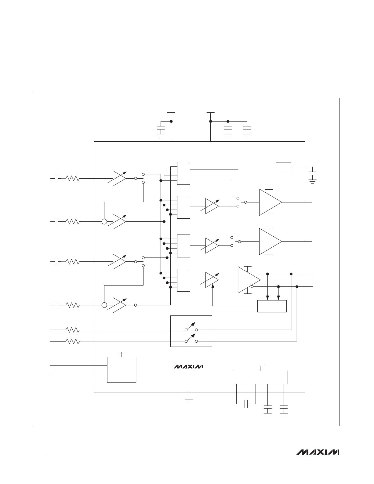
Functional Diagram/Typical Application Circuit
1.6V TO 2V 2.7V TO 5.5V
1µF 0.1µF 10µF
V
DD
B4
PVDD
D4
MAX97002
0.47µF
0.47µF
0.47µF
0.47µF
OPTIONAL
OPTIONAL
OPTIONAL
OPTIONAL
INA1
INA2
INB1 D1
INB2 D2
COM1 C3
COM2 D3
PGAINA
-6dB TO +18dB
C1
PGAINA
-6dB TO +18dB
C2
+
PGAINB
-6dB TO +18dB
PGAINB
-6dB TO +18dB
INADIFF
INBDIFF
MUX
LPMODE
MIX
HPLMIX
MIX
HPRMIX
MIX
SPKMIX
HPLVOL:
-64dB TO +6dB
HPRVOL:
-64dB TO +6dB
SPKVOL:
-30dB TO +20dB
CLASS H
CLASS H
PVDD
CLASS D
+12dB
SPKEN
PGND
+
ANALOG SWITCHES
HPVDD
0/3dB
HPLEN
HPVSS
HPVDD
0/3dB
HPREN
HPVSS
THD LIMITER
LMTEN
BIAS
B1
BIAS
1µF
HPLA2
HPRA1
C5
OUTP
OUTN
D5
V
SDA B2
SCL B3
DD
2
I
C
INTERFACE
BYPEN
MAX97002
C4
GND
A4
C1P
V
DD
CHARGE PUMP
A5
C1N
B5
A3
HPVDD HPVSS
4
Page 5
Audio Subsystem with Mono Class D
Speaker and Class H Headphone Amplifiers
ABSOLUTE MAXIMUM RATINGS
(Voltages with respect to GND.)
V
, HPVDD ........................................................-0.3V to +2.2V
DD
PVDD ....................................................................-0.3V to +6.0V
HPVSS ..................................................................-2.2V to +0.3V
C1N .....................................(HPVSS - 0.3V) to (HPVDD + 0.3V)
C1P ...................................................... -0.3V to (HPVDD + 0.3V)
HPL, HPR ............................ (HPVSS - 0.3V) to (HPVDD + 0.3V)
INA1, INA2, INB1, INB2, BIAS ............................. -0.3V to +6.0V
SDA, SCL .............................................................-0.3V to +6.0V
COM1, COM2, OUTP, OUTN .................-0.3V to (PVDD + 0.3V)
Continuous Current In/Out of PVDD, GND, OUT_ ........ Q800mA
Continuous Current In/Out of HPR, HPL, VDD .............. Q140mA
Continuous Current In/Out of COM1, COM2 ................ Q150mA
Stresses beyond those listed under “Absolute Maximum Ratings” may cause permanent damage to the device. These are stress ratings only, and functional
operation of the device at these or any other conditions beyond those indicated in the operational sections of the specifications is not implied. Exposure to absolute
maximum rating conditions for extended periods may affect device reliability.
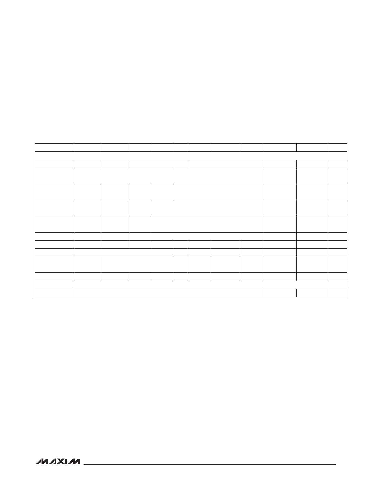
ELECTRICAL CHARACTERISTICS
(V
= 1.8V, V
VDD
HPRVOL = SPKVOL = 0dB, speaker loads (Z
HPL or HPR to GND. SDA and SCL pullup voltage = 1.8V. Z
T
= T
MIN
to T
MAX
A
PARAMETER SYMBOL CONDITIONS MIN TYP MAX UNITS
Speaker Amplifier Supply
Voltage Range
Headphone Amplifier Supply
Voltage Range
Quiecsent Supply Current
Shutdown Current I
Turn-On Time t
Input Resistance R
PVDD
= 3.7V, V
= 0V. Input signal applied at INA configured single-ended, preamp gain = 0dB, HPLVOL =
GND
) connected between OUTP and OUTN. Headphone loads (RHP) connected from
SPK
, unless otherwise noted. Typical values are at TA = +25NC.) (Note 1)
PVDD Guaranteed by PSRR test 2.7 5.5 V
V
DD
Guaranteed by PSRR test 1.6 2 V
Low-power headphone
mode, T
HP mode, T
= +25NC
A
A
stereo SE input on INA,
INB disabled
SPK mode, T
mono differential Input on
INB, INA disabled
SPK + HP mode, T
+25NC, stereo SE input on
INA, INB disabled
SHDN
ON
IN
TA = +25NC, V
Time from power-on to full operation,
including soft-start
TA = +25NC,
internal gain
Continuous Input Current (all other pins) ........................ Q20mA
Duration of OUT_ Short Circuit to GND or PVDD .....Continuous
Duration of Short Circuit Between
OUTP and OUTN ................................................... Continuous
Duration of HP_ Short Circuit to GND or V
Continuous Power Dissipation (T
= +70NC)
A
...........Continuous
DD
20-Bump WLP Multilayer Board
(derate 13mW/NC above +70NC)................................1040mW
Junction Temperature .....................................................+150NC
Operating Temperature Range .......................... -40NC to +85NC
Storage Temperature Range ............................ -65NC to +150NC
Lead Temperature (soldering, 10s) ................................+260NC
= J, RHP = J. C
SPK
= +25NC,
= +25NC
A
=
A
= 0V
SHDN
C1P-C1N
I
VDD
I
PVDD
I
VDD
I
PVDD
I
VDD
I
PVDD
I
VDD
I
PVDD
I
VDD + IPVDD
V
= 0V,
VDD
I
PVDD
= C
HPVDD
= C
1.35 1.85
0.35 0.55
1.35 1.85
0.75 1.15
0.32 0.6
1.38 2.2
1.35 1.85
1.8 2.7
< 1
HPVSS
0 8
10 ms
Gain = -6dB, -3dB 41.2
Gain = 0dB, 3dB,
6dB, dB
16 20.6 27
Gain = 18dB 5.5 7.2 9.6
= C
BIAS
= 1FF.
mA
FA
kI
MAX97002
5
Page 6

Audio Subsystem with Mono Class D
Speaker and Class H Headphone Amplifiers
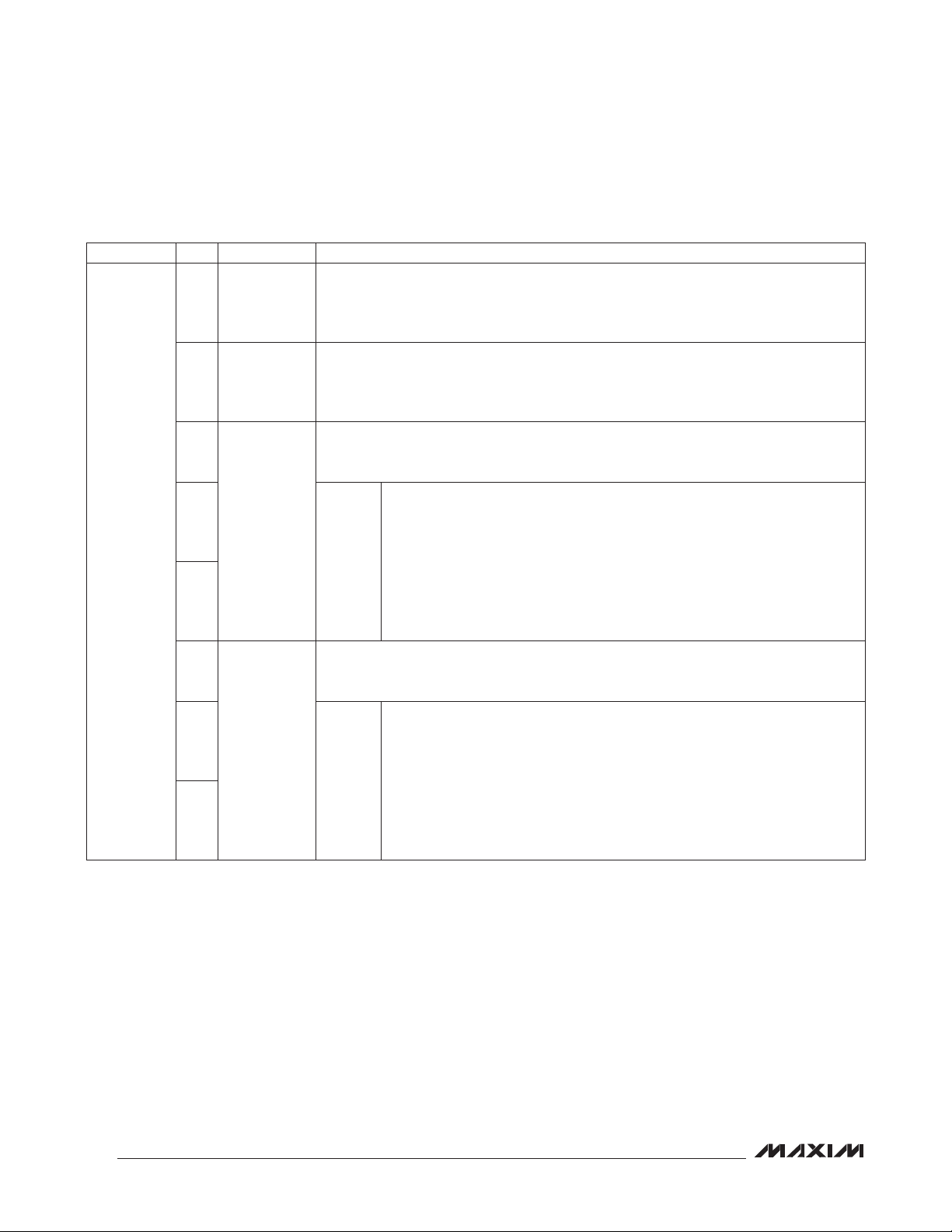
ELECTRICAL CHARACTERISTICS (continued)
(V
= 1.8V, V
VDD
HPRVOL = SPKVOL = 0dB, speaker loads (ZSPK) connected between OUTP and OUTN. Headphone loads (RHP) connected from
HPL or HPR to GND. SDA and SCL pullup voltage = 1.8V. ZSPK = J, RHP = J. C
T
= T
A
Feedback Resistance R
MAX97002
Maximum Input Signal Swing
Common-Mode Rejection
Ratio
Input DC Voltage IN__ inputs 1.125 1.2 1.275 V
Bias Voltage V
SPEAKER AMPLIFIER
Output Offset Voltage V
Click-and-Pop Level K
Power-Supply Rejection Ratio
(Note 2)
Output Power (Note 3)
Total Harmonic Distortion
Plus Noise
Signal-to-Noise Ratio SNR
to T
MIN
MAX
PARAMETER SYMBOL CONDITIONS MIN TYP MAX UNITS
= 3.7V, V
PVDD
, unless otherwise noted. Typical values are at TA = +25NC.) (Note 1)
= 0V. Input signal applied at INA configured single-ended, preamp gain = 0dB, HPLVOL =
GND
F
CMRR
BIAS
OS
CP
PSRR
THD+N
TA = +25NC, external gain
Preamp = 0dB 2.3
Preamp = +18dB 0.29
Preamp = external gain
f = 1kHz (differential input mode),
gain = 0dB
f = 1kHz (differential input mode),
gain = 18dB
1.13 1.2 1.27 V
TA = +25NC, SPKM = 1 Q0.5 Q4
T
= +25NC, SPKMIX = 0x01, IN_DIFF = 0 Q1.5
A
Peak voltage, TA =
+25NC, A-weighted,
32 samples per second, volume at mute
(Note 2)
T
= +25NC
A
THD+N P 1%,
f = 1kHz,
Z
= 8I + 68FH
SPK
f = 1kHz, P
R
= 8I
SPK
A-weighted,
SPKMIX = 0x03, referenced to 700mW
= 360mW, TA = +25NC,
OUT
Into shutdown -70
Out of shutdown -70
= 2.7V to
V
PVDD
5.5V
f = 217Hz,
200mV
P-P
f = 1kHz,
200mV
P-P
f = 20kHz,
200mV
P-P
= 4.2V 920
V
PVDD
= 3.7V 700
PVDD
= 3.3V 550
V
PVDD
IN_DIFF = 0
(single-ended)
IN_DIFF = 1
(differential)
C1P-C1N
ripple
ripple
ripple
= C
= C
HPVDD
19 20 21
2.3 x
RINEX/RF
55
32
50 77
73
73
57
0.05 0.6 %
96
96
HPVSS
= C
BIAS
= 1FF.
kI
V
P-P
dB
mV
dBV
dB
mWV
dB
6
Page 7
Audio Subsystem with Mono Class D
Speaker and Class H Headphone Amplifiers
ELECTRICAL CHARACTERISTICS (continued)
(V
= 1.8V, V
VDD
HPRVOL = SPKVOL = 0dB, speaker loads (ZSPK) connected between OUTP and OUTN. Headphone loads (RHP) connected from
HPL or HPR to GND. SDA and SCL pullup voltage = 1.8V. ZSPK = J, RHP = J. C
T
= T
MIN
to T
MAX
A
PARAMETER SYMBOL CONDITIONS MIN TYP MAX UNITS
Oscillator Frequency f
Spread-Spectrum Bandwidth
Gain 11.5 12 12.5 dB
Current Limit 1.5 A
Efficiency
Output Noise
CHARGE PUMP
Charge-Pump Frequency
Positive Output Voltage V
Negative Output Voltage V
Headphone Output Voltage
Threshold
Mode Transition Timeouts
HEADPHONE AMPLIFIERS
Output Offset Voltage V
Click-and-Pop Level K
PVDD
= 3.7V, V
= 0V. Input signal applied at INA configured single-ended, preamp gain = 0dB, HPLVOL =
GND
, unless otherwise noted. Typical values are at TA = +25NC.) (Note 1)
OSC
E
250 kHz
= 600mW, f = 1kHz 87 %
P
OUT
A-weighted, (SPKMIX = 0x01),
IN_DIFF = 1, SPKVOL = -30dB
V
HPVDD
HPVSS
V
TH1
V
TH2
= V
HPL
= V
HPL
= V
V
HPL
V
, V
HPL
, V
V
HPL
V
, V
HPL
, V
V
HPL
Output voltage at which the charge pump
switches between fast and slow clock
Output voltage at which the charge pump
switches modes, VOUT rising or falling
= 0V, TA = +25NC
HPR
= 0.2V 665
HPR
= 0.5V 500
HPR
> V
HPR
HPR
HPR
HPR
< V
> V
< V
TH
TH
TH
TH
Time it takes for the charge pump to transition from Invert to split mode
Time it takes for the charge pump to transition from split to invert mode
OS
CP
TA = +25NC, volume at mute
T
= +25NC, HP_MIX = 0x1, IN_DIFF = 0
A
Peak voltage, TA =
+25NC, A-weighted, 32
samples per second,
volume at mute (Note 2)
Into shutdown -74
Out of shutdown
C1P-C1N
= C
HPVDD
= C
Q20
37
80 83 85
V
DD
VDD/2
-V
DD
-VDD/2
QV
QVDD
DD
x 0.05
QV
x 0.21
DD
x 0.08
QVDD
x 0.25
32 ms
20
Q0.15 Q0.6
Q0.5
-74
HPVSS
= C
BIAS
kHz
QVDD
x 0.13
QVDD
x 0.3
= 1FF.
FV
RMS
kHzV
V
V
V
Fs
mV
dBV
MAX97002
7
Page 8
Audio Subsystem with Mono Class D
Speaker and Class H Headphone Amplifiers
ELECTRICAL CHARACTERISTICS (continued)
(V
= 1.8V, V
VDD
HPRVOL = SPKVOL = 0dB, speaker loads (ZSPK) connected between OUTP and OUTN. Headphone loads (RHP) connected from
HPL or HPR to GND. SDA and SCL pullup voltage = 1.8V. ZSPK = J, RHP = J. C
T
= T
MIN
to T
MAX
A
PARAMETER SYMBOL CONDITIONS MIN TYP MAX UNITS
MAX97002
Power-Supply Rejection Ratio
(Note 2)
Output Power P
Channel-to-Channel Gain
Tracking
Total Harmonic Distortion
Plus Noise
Signal-to-Noise Ratio SNR
Slew Rate SR 0.35
Capacitive Drive C
Crosstalk
ANALOG SWITCH
On-Resistance R
Total Harmonic Distortion
Plus Noise
Off-Isolation
PVDD
= 3.7V, V
= 0V. Input signal applied at INA configured single-ended, preamp gain = 0dB, HPLVOL =
GND
, unless otherwise noted. Typical values are at TA = +25NC.) (Note 1)
= 1.62V to
V
DD
1.98V
f = 217Hz,
V
RIPPLE
200mV
PSRR
= +25NC
T
A
f = 1kHz,
V
RIPPLE
200mV
f = 20kHz,
V
RIPPLE
200mV
= 16I
R
THD+N = 1%, f = 1kHz
OUT
T
= +25NC, HPL to HPR, HPLMIX = 0x01,
THD+N P
A
HPRMIX = 0x02, IN_DIFF = 0
= 10mW, f = 1kHz
OUT
A-weighted, R
= 16I, HPLMIX = 0x01,
HP
R
R
R
HP
HP
HP
HP
= 32I
= 32I
= 16I
HPRMIX = 0x02, IN_DIFF = 0
L
200 pF
HPL to HPR, HPR to HPL, f = 20Hz to
20kHz
T
= +25NC
A
T
= T
A
T
MAX
10I in series
with each
switch
No series
resistors
ON
THD+N
I
= 20mA, V
NC_
COM_
=
0V and PVDD, SWEN = 1
V
DIFCOM_
V
CMCOM_
= 2V
P-P
= PVDD/2,
,
f = 1kHz, SWEN = 1,
Z
= 8I + 68FH
SPK
SWEN = 0, COM1 and COM2 to GND = 50I,
f = 10kHz, referred to signal applied to
OUTP and OUTN
C1P-C1N
=
P-P
=
P-P
=
P-P
to
MIN
= C
HPVDD
= C
HPVSS
= C
70 85
84
80
69
37
30
Q0.3 Q2.5
0.02
0.03 0.1
100 dB
68 dB
1.6 4
5.2
0.05
0.3
90 dB
BIAS
= 1FF.
dB
mW
%
%
V/Fs
I
%
8
Page 9
Audio Subsystem with Mono Class D
Speaker and Class H Headphone Amplifiers
ELECTRICAL CHARACTERISTICS (continued)
(V
= 1.8V, V
VDD
HPRVOL = SPKVOL = 0dB, speaker loads (ZSPK) connected between OUTP and OUTN. Headphone loads (RHP) connected from
HPL or HPR to GND. SDA and SCL pullup voltage = 1.8V. ZSPK = J, RHP = J. C
T
= T
A
PREAMPLIFIER
Gain
VOLUME CONTROL
Volume Level
Mute Attenuation f = 1kHz
Zero-Crossing Detection
Timeout
LIMITER
Attack Time 1 ms
Release Time Constant
to T
MIN
MAX
PARAMETER SYMBOL CONDITIONS MIN TYP MAX UNITS
= 3.7V, V
PVDD
, unless otherwise noted. Typical values are at TA = +25NC.) (Note 1)
= 0V. Input signal applied at INA configured single-ended, preamp gain = 0dB, HPLVOL =
GND
PGAIN_ = 000 -6.5 -6 -5.5
PGAIN_ = 001 -3.5 -3 -2.5
PGAIN_ = 010 -0.5 0 +0.5
100 ms
PGAIN_ = 011 2.5 3 3.5
PGAIN_ = 100 5.5 6 6.5
PGAIN_ = 101 8.5 9 9.5
PGAIN_ = 110 17.5 18 18.5
HP_VOL = 0x1F 5.5 6 6.5
HP_VOL = 0x00 -68 -64 -60
SPKVOL = 0x3F 19 20 21
SPKVOL = 0x00 -31 -30 -29
Speaker 100
Headphone 110
THDT1 = 0 1.4
THDT1 = 1 2.8
C1P-C1N
= C
HPVDD
= C
HPVSS
= C
BIAS
= 1FF.
dB
dB
dB
s
MAX97002
DIGITAL I/O CHARACTERISTICS
(V
= 3.7V, V
PVDD
PARAMETER SYMBOL CONDITIONS MIN TYP MAX UNITS
DIGITAL INPUTS (SDA, SCL)
Input Voltage High V
Input Voltage Low V
Input Hysteresis V
Input Capacitance C
Input Leakage Current I
DIGITAL OUTPUTS (SDA Open Drain)
Output Low Voltage V
= 0V. TA = T
GND
MIN
to T
HYS
IH
IL
IN
IN
OL
MAX
I
, unless otherwise noted. Typical values are at TA = +25NC.) (Note 1)
TA = +25NC
= 3mA 0.4 V
SINK
0.75 x
V
DD
200 mV
10 pF
V
0.35 x
V
DD
±1.0
V
FA
9
Page 10
Audio Subsystem with Mono Class D
Speaker and Class H Headphone Amplifiers
I2C TIMING CHARACTERISTICS
(V
= 3.7V, V
PVDD
PARAMETER SYMBOL CONDITIONS MIN TYP MAX UNITS
Serial-Clock Frequency f
Bus Free Time Between STOP
and START Conditions
Hold Time (Repeated) START
Condition
MAX97002
SCL Pulse-Width Low t
SCL Pulse-Width High t
Setup Time for a REPEATED
START Condition
Data Hold Time t
Data Setup Time t
SDA and SCL Receiving Rise
Time
SDA and SCL Receiving Fall
Time
SDA Transmitting Fall Time t
Setup Time for STOP Condition t
Bus Capacitance C
Pulse Width of Suppressed
Spike
Note 1: 100% production tested at T
Note 2: Amplifier inputs are AC-coupled to GND.
Note 3: Class D amplifier testing performed with a resistive load in series with an inductor to simulate an actual speaker load.
Note 4: C
is in pF.
B
= 0V. TA = T
GND
to T
MIN
t
HD,STA
t
SU,STA
HD,DAT
SU,DAT
SU,STO
= +25NC. Specifications over temperature limits are guaranteed by design.
A
, unless otherwise noted. Typical values are at TA = +25NC.) (Note 1)
MAX
SCL
t
BUF
0 400 kHz
1.3 Fs
0.6 Fs
LOW
HIGH
1.3 Fs
0.6 Fs
0.6 Fs
0 900 ns
100 ns
t
R
t
F
F
(Note 4)
(Note 4)
(Note 4)
20 +
0.1C
20 +
0.1C
20 +
0.1C
0.6 Fs
B
t
SP
400 pF
0 50 ns
B
B
B
300 ns
300 ns
300 ns
Figure 1. I
10
CONDITION
SCL
SDA
2
C Interface Timing Diagram
START
28 9
1
CLOCK PULSE FOR
ACKNOWLEDGMENT
NOT ACKNOWLEDGE
ACKNOWLEDGE
Page 11
Audio Subsystem with Mono Class D
Speaker and Class H Headphone Amplifiers
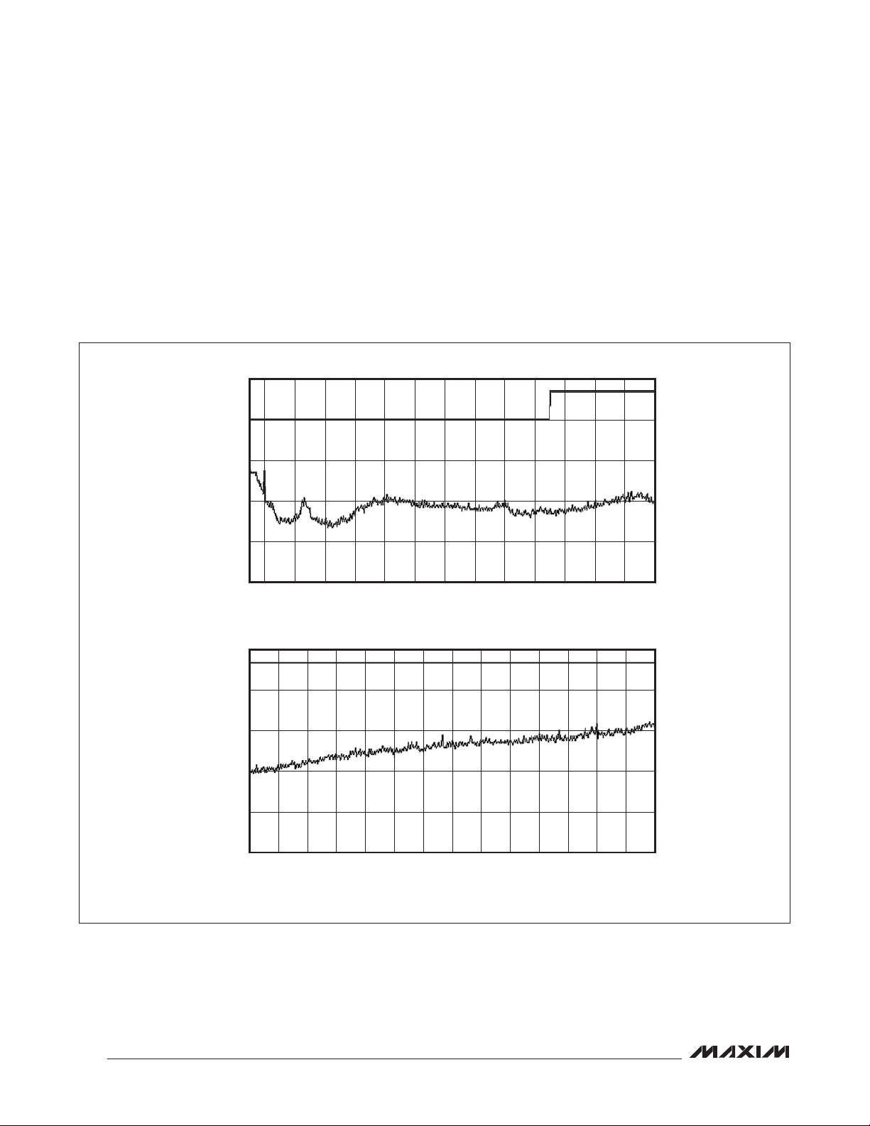
Typical Operating Characteristics
(V
= V
LDOIN
loads (ZSPK) connected between OUTP and OUTN. Headphone loads (RHP) connected from HPL or HPR to GND. ZSPK = ∞, RHP = ∞.
C
C1P-C1N
6
5
4
3
2
SUPPLY CURRENT (mA)
1
0
2.5 5.5
10
0
-10
-20
-30
-40
-50
-60
HEADPHONE VOLUME ATTENUATION (dB)
-70
0 35
PVDD
= C
= 3.7V, V
HPVDD
= C
GND
HPVSS
= V
= C
PGND
BIAS
SUPPLY CURRENT
vs. SUPPLY VOLTAGE
SPEAKER ONLY
INPUTS AC-COUPLED TO GND
INPUT = INA
V
= V
= 3.3V
SDA
SCL
5.04.54.03.53.0
SUPPLY VOLTAGE (V)
HEADPHONE VOLUME ATTENUATION
vs. HP_VOL CODE
RIGHT AND LEFT
32I LOAD
30255 10 15 20
HP_VOL CODE (NUMERIC)
= 0V. Single-ended inputs, preamp gain = 0dB, HPLVOL = HPRVOL = SPKVOL = 0dB. Speaker
= 1μF. TA = +25°C, unless otherwise noted.)
4.0
3.5
MAX97002 toc01
3.0
2.5
2.0
1.5
SHUTDOWN CURRENT (µA)
1.0
0.5
0
2.5 5.5
10
MAX97002 toc04
1
0.1
THD+N (%)
0.01
0.001
0.01 100
SHUTDOWN CURRENT
vs. SUPPLY VOLTAGE
INPUTS AC-COUPLED TO GND
V
= V
= 3.3V
SDA
SCL
SUPPLY VOLTAGE (V)
THD+N vs. FREQUENCY
V
= 3.7V
PVDD
Z
= 8I + 68µF
SPRK
P
= 600mW
OUT
P
OUT
FREQUENCY (kHz)
MAX97002 toc02
5.04.54.03.53.0
MAX97002 toc05
= 200mW
1010.1
SPEAKER VOLUME ATTENUATION
vs. VOLUME CONTROL CODE
30
8I LOAD
20
10
0
-10
-20
SPEAKER VOLUME ATTENUATION (dB)
-30
-40
0 70
VOLUME CONTROL CODE (NUMERIC)
THD+N vs. FREQUENCY
10
V
= 3.7V
PVDD
Z
= 4I + 33µF
SPRK
1
P
= 1000mW
OUT
0.1
THD+N (%)
P
= 200mW
0.01
0.001
0.01 100
FREQUENCY (kHz)
OUT
605040302010
1010.1
MAX97002
MAX97002 toc03
MAX97002 toc06
10
THD+N vs. FREQUENCY
V
= 3.7V
PVDD
Z
= 8I + 68µF
SPRK
1
0.1
THD+N (%)
SSM
0.01
FFM
0.001
0.01 100
FREQUENCY (kHz)
THD+N vs. OUTPUT POWER
MAX97002 toc08
100
10
THD+N (%)
0.1
0.01
0.001
100
V
= 5.0V
PVDD
Z
= 8I + 68µF
SPRK
10
MAX97002 toc07
fIN = 1kHz
0 400
fIN = 6kHz
fIN = 100Hz
800 1200 1600 2000
P
(mW)
OUT
2400
1
THD+N (%)
0.1
0.01
1010.1
0.001
THD+N vs. OUTPUT POWER
= 5.0V
V
PVDD
Z
= 4I + 33µF
SPRK
1
fIN = 6kHz
fIN = 1kHz
fIN = 100Hz
0 4000
P
(mW)
OUT
350030002500200015001000500
MAX97002 toc09
11
Page 12
Audio Subsystem with Mono Class D
Speaker and Class H Headphone Amplifiers
Typical Operating Characteristics (continued)
(V
= V
LDOIN
loads (ZSPK) connected between OUTP and OUTN. Headphone loads (RHP) connected from HPL or HPR to GND. ZSPK = ∞, RHP = ∞.
C
C1P-C1N
PVDD
= C
= 3.7V, V
HPVDD
= C
GND
HPVSS
= V
= C
= 0V. Single-ended inputs, preamp gain = 0dB, HPLVOL = HPRVOL = SPKVOL = 0dB. Speaker
PGND
= 1μF. TA = +25°C, unless otherwise noted.)
BIAS
100
V
= 4.2V
PVDD
Z
= 8I + 68µF
SPRK
10
MAX97002
THD+N vs. OUTPUT POWER
1
THD+N (%)
0.1
0.01
0.001
100
10
1
THD+N (%)
0.1
0.01
0.001
fIN = 6kHz
fIN = 1kHz
0 1600
P
OUT
THD+N vs. OUTPUT POWER
V
= 3.7V
PVDD
Z
= 4I + 33µF
SPRK
fIN = 6kHz
fIN = 1kHz
0 400
800
P
OUT
fIN = 100Hz
140012001000800600400200
(mW)
f
= 100Hz
IN
1200 1600 2000
(mW)
MAX97002 toc10
MAX97002 toc13
100
V
= 4.2V
PVDD
Z
= 4I + 33µF
SPRK
10
fIN = 1kHz
fIN = 6kHz
fIN = 100Hz
P
(mW)
OUT
1
THD+N (%)
0.1
0.01
0.001
EFFICIENCY vs. OUTPUT POWER
100
Z
= 8I + 68µF
SPRK
90
80
THD+N vs. OUTPUT POWER
70
60
50
40
EFFICIENCY (%)
30
20
10
0
0 2.5
Z
SPRK
P
(W)
OUT
25002000150010005000 3000
= 4I + 33µF
V
= 5.0V
PVDD
fIN = 1kHz
2.01.51.00.5
MAX97002 toc11
MAX97002 toc14
100
V
PVDD
Z
SPRK
10
1
0.01
fIN = 1kHz
0.1
THD+N (%)
0.001
EFFICIENCY vs. OUTPUT POWER
100
Z
SPRK
90
80
70
60
50
40
EFFICIENCY (%)
30
20
10
0
THD+N vs. OUTPUT POWER
= 3.7V
= 8I + 68µF
fIN = 6kHz
fIN = 100Hz
P
(mW)
OUT
= 8I + 68µF
Z
= 4I + 33µF
SPRK
V
PVDD
fIN = 1kHz
P
(W)
OUT
MAX97002 toc12
120010008006004002000
MAX97002 toc15
= 3.7V
1.41.20.8 1.00.4 0.60.20 1.6
OUTPUT POWER vs. SUPPLY VOLTAGE
2.0
fIN = 1kHz
1.8
Z
= 8I + 68µF
SPRK
1.6
1.4
1.2
1.0
0.8
OUTPUT POWER (W)
0.6
0.4
0.2
0
THD+N = 10%
2.5 5.5
SUPPLY VOLTAGE (V)
12
THD+N = 1%
OUTPUT POWER vs. SUPPLY VOLTAGE
3.5
fIN = 1kHz
Z
3.0
MAX97002 toc16
2.5
2.0
1.5
OUTPUT POWER (W)
1.0
0.5
5.04.53.0 3.5 4.0
0
= 4I + 33µF
SPRK
THD+N = 10%
THD+N = 1%
2.5 5.5
SUPPLY VOLTAGE (V)
5.04.54.03.53.0
MAX97002 toc17
OUTPUT POWER vs. LOAD RESISTANCE
2.0
1.8
1.6
1.4
1.2
1.0
0.8
OUTPUT POWER (W)
0.6
THD+N = 1%
0.4
0.2
0
LOAD RESISTANCE (I)
V
PVDD
f
= 1kHz
IN
Z
SPRK
THD+N = 10%
= 3.7V
= LOAD + 68µF
100101 1000
MAX97002 toc18
Page 13

Audio Subsystem with Mono Class D
Speaker and Class H Headphone Amplifiers
Typical Operating Characteristics (continued)
(V
= V
LDOIN
loads (ZSPK) connected between OUTP and OUTN. Headphone loads (RHP) connected from HPL or HPR to GND. ZSPK = ∞, RHP = ∞.
C
C1P-C1N
0
-10
-20
-30
-40
-50
PSRR (dB)
-60
-70
-80
-90
-100
0.01 100
PVDD
= C
= 3.7V, V
HPVDD
= C
GND
HPVSS
= V
= C
PGND
BIAS
POWER-SUPPLY REJECTION RATIO
vs. FREQUENCY
V
= 200mV
RIPPLE
V
PVDD
INPUTS AC-COUPLED GND
= 3.7V
FREQUENCY (kHz)
P-P
1010.1
= 0V. Single-ended inputs, preamp gain = 0dB, HPLVOL = HPRVOL = SPKVOL = 0dB. Speaker
= 1μF. TA = +25°C, unless otherwise noted.)
MAX97002 toc19
POWER-SUPPLY REJECTION RATIO
vs. SUPPLY VOLTAGE
0
V
= 200mV
RIPPLE
fIN = 1kHz
-20
INPUTS AC-COUPLED GND
-40
PSRR (dB)
-60
-80
-100
2.5 5.5
P-P
SUPPLY VOLTAGE (V)
MAX97002 toc20
AMPLITUDE (dBV)
-100
-120
5.04.54.03.53.0
IN-BAND OUTPUT SPECTRUM
0
SSM
-20
-40
-60
-80
= 1kHz
f
IN
0 20
FREQUENCY (kHz)
15105
MAX97002
MAX97002 toc21
IN-BAND OUTPUT SPECTRUM
0
FFM
-20
-40
-60
AMPLITUDE (dBV)
-80
-100
-120
= 1kHz
f
IN
0 20
FREQUENCY (kHz)
WIDEBAND OUTPUT SPECTRUM
0
-10
-20
-30
-40
-50
-60
-70
OUTPUT AMPLITUDE (dBV)
-80
-90
-100
0.1 1000
FREQUENCY (MHz)
RBW = 100Hz
SSM
WIDEBAND OUTPUT SPECTRUM
0
MAX97002 toc22
15105
-20
-40
-60
-80
OUTPUT AMPLITUDE (dBV)
-100
-120
0.1 1000
FREQUENCY (MHz)
SOFTWARE SHUTDOWN RESPONSE
MAX97002 toc24
100101
1ms/div
RBW = 100Hz
FFM
100101
MAX97002 toc25
MAX97002 toc23
SDA
2V/div
SPKR
OUTPUT
200mA/div
13
Page 14

Audio Subsystem with Mono Class D
Speaker and Class H Headphone Amplifiers
Typical Operating Characteristics (continued)
(V
= V
LDOIN
loads (ZSPK) connected between OUTP and OUTN. Headphone loads (RHP) connected from HPL or HPR to GND. ZSPK = ∞, RHP = ∞.
C
C1P-C1N
PVDD
= C
= 3.7V, V
HPVDD
= C
GND
HPVSS
= V
= C
= 0V. Single-ended inputs, preamp gain = 0dB, HPLVOL = HPRVOL = SPKVOL = 0dB. Speaker
PGND
= 1μF. TA = +25°C, unless otherwise noted.)
BIAS
SOFTWARE TURN-ON RESPONSE
MAX97002
2ms/div
10
0.1
THD+N (%)
0.01
0.001
THD+N vs. OUTPUT POWER
R
LOAD
1
fIN = 1kHz
0 4035
MAX97002 toc26
= 32I
fIN = 6kHz
OUTPUT POWER (mW)
SDA
2V/div
SPKR
OUTPUT
200mA/div
fIN = 100Hz
30252015105
10
THD+N vs. FREQUENCY
R
= 32I
LOAD
1
0.1
THD+N (%)
0.01
0.001
0.01 100
MAX97002 toc29
P
= 25mW
OUT
FREQUENCY (kHz)
P
= 5mW
OUT
10
R
= 16I
LOAD
MAX97002 toc27
1010.1
1
P
= 30mW
OUT
0.1
THD+N (%)
P
= 10mW
0.01
0.001
0.01 100
OUT
FREQUENCY (kHz)
1010.1
MAX97002 toc28
THD+N vs. OUTPUT POWER
10
R
= 16I
LOAD
THD+N vs. FREQUENCY
1
fIN = 6kHz
0.1
THD+N (%)
0.01
0.001
fIN = 1kHz
0 70
OUTPUT POWER (mW)
fIN = 100Hz
MAX97002 toc30
605040302010
14
POWER DISSIPATION
vs. OUTPUT POWER
110
fIN = 1kHz
100
P
90
80
70
60
50
40
30
POWER DISSIPATION (mW)
20
10
0
0 140
= P
OUT
HPL
OUTPUT POWER (mW)
+ P
HPR
R
LOAD
R
= 32I
LOAD
= 16I
1201008040 6020
MAX97002 toc31
OUTPUT POWER vs. LOAD RESISTANCE
250
200
THD+N = 10%
150
100
OUTPUT POWER (mW)
THD+N = 1%
50
0
1 1000
LOAD RESISTANCE (I)
10010
f
IN
= 1kHz
MAX97002 toc32
Page 15

Audio Subsystem with Mono Class D
Speaker and Class H Headphone Amplifiers
Typical Operating Characteristics (continued)
(V
= V
LDOIN
loads (ZSPK) connected between OUTP and OUTN. Headphone loads (RHP) connected from HPL or HPR to GND. ZSPK = ∞, RHP = ∞.
C
C1P-C1N
OUTPUT POWER vs. LOAD RESISTANCE
90
80
70
60
50
40
30
OUTPUT POWER (W)
20
10
0
1 1000
= 3.7V, V
PVDD
= C
HPVDD
fIN = 1kHz
THD+N = 1%
MEASURED AT
HPR ONLY
LOAD RESISTANCE (I)
GND
= C
HPVSS
C1 = C2 = C3 = 2.2µF
C1 = C2 = C3 = 1µF
10010
= V
= C
= 0V. Single-ended inputs, preamp gain = 0dB, HPLVOL = HPRVOL = SPKVOL = 0dB. Speaker
PGND
= 1μF. TA = +25°C, unless otherwise noted.)
BIAS
POWER-SUPPLY REJECTION RATIO
OUTPUT SPECTRUM
R
= 32I
LOAD
f
= 1kHz
IN
FREQUENCY (kHz)
MAX97002 toc33
0
vs. FREQUENCY
V
= 200mV
RIPPLE
VDD = 1.8V
-20
INPUTS AC-COUPLED GND
-40
-60
PSRR (dB)
-80
-100
-120
-140
0.01 100
P-P
FREQUENCY (kHz)
0
-20
MAX97002 toc34
-40
-60
-80
AMPLITUDE (dBV)
-100
-120
-140
1010.1
0 20
16 181442 6 8 10 12
MAX97002
MAX97002 toc35
0
R
= 16I
LOAD
f
= 1kHz
-20
IN
-40
-60
-80
AMPLITUDE (dBV)
-100
-120
-140
0 14 16 18 20
FREQUENCY (kHz)
121082 4 6
COMMON-MODE REJECTION RATIO
vs. FREQUENCY
0
R
= 32I
LOAD
-10
OUTPUT SPECTRUM
-20
-30
-40
CROSSTALK (dB)
-50
-60
PREGAIN = +18dB
PREGAIN = +9dB
PREGAIN = 0dB
MAX97002 toc36
MAX97002 toc38
CROSSTALK vs. FREQUENCY
0
R
= 32I
LOAD
-10
-20
-30
-40
-50
CROSSTALK (dB)
-60
LEFT TO RIGHT
-70
-80
-90
0.01 100
RIGHT TO LEFT
FREQUENCY (kHz)
SOFTWARE SHUTDOWN RESPONSE
MAX97002 toc37
1010.1
MAX97002 toc39
SDA
2V/div
HPL/HPR
200mV/div
-70
0.01 100
FREQUENCY (kHz)
1010.1
1ms/div
15
Page 16
Audio Subsystem with Mono Class D
Speaker and Class H Headphone Amplifiers
Typical Operating Characteristics (continued)
(V
loads (ZSPK) connected between OUTP and OUTN. Headphone loads (RHP) connected from HPL or HPR to GND. ZSPK = ∞, RHP = ∞.
C
LDOIN
C1P-C1N
= V
PVDD
= C
= 3.7V, V
HPVDD
= C
GND
HPVSS
= V
= C
= 0V. Single-ended inputs, preamp gain = 0dB, HPLVOL = HPRVOL = SPKVOL = 0dB. Speaker
PGND
= 1μF. TA = +25°C, unless otherwise noted.)
BIAS
SOFTWARE STARTUP RESPONSE
MAX97002
2ms/div
3.5
INC = 20mA
3.0
2.5
2.0
(I)
ON
R
1.5
1.0
0.5
MAX97002 toc40
SDA
2V/div
HPL/HPR
200mV/div
ON-RESISTANCE vs. V
V
= 2.5V
PVDD
V
= 2.7V
PVDD
V
= 3.0V
PVDD
V
PVDD
V
= 5.0V
PVDD
V
0V
0V
COM
= 3.7V
PVDD
= 5.5V
CLASS H OPERATION
10ms/div
MAX97002 toc43
MAX97002 toc41
HPVDD
1V/div
HPL/HPR
200mV/div
HPVSS
1V/div
BYPASS SWITCH OFF-ISOLATION
0
-20
-40
-60
-80
OFF-ISOLATION (dB)
-100
THD+N vs. OUTPUT POWER
10
R
= 8I
LOAD
EXTERNAL CLASS AB
CONNECTED DIRECTLY
1
TO COM1 AND COMR
f = 6kHz
0.1
THD+N (%)
0.01
0.001
0 80
f = 100Hz
f = 1kHz
OUTPUT POWER (mW)
MAX97002 toc42
70605040302010
MAX97002 toc44
16
0
0 6
V
(V)
COM
54321
-120
0.01 100
FREQUENCY (kHz)
1010.1
Page 17
Audio Subsystem with Mono Class D
Speaker and Class H Headphone Amplifiers
Pin Configuration
TOP VIEW
(BUMP SIDE DOWN)
MAX97002
2 3 41
+
MAX97002
A
B
C
INA1
D
HPL HPVSS C1PHPR
SDA V
INA2 COM1 GND OUTP
INB2 COM2 PVDD OUTNINB1
SCLBIAS
DD
5
C1N
HPVDD
Pin Description
PIN NAME DESCRIPTION
A1 HPR Headphone Amplifier Left Output
A2 HPL Headphone Amplifier Right Output
A3 HPVSS
A4 C1P
A5 C1N
B1 BIAS
B2 SDA Serial-Data Input/Output. Connect a pullup resistor from SDA to DVDD.
B3 SCL Serial-Clock Input. Connect a pullup resistor from SCL to DVDD.
B4 V
B5 HPVDD
C1 INA1 Input A1. Left input or negative input.
C2 INA2 Input A2. Right input or positive input.
C3 COM1 Positive Bypass Switch Input
C4 GND Analog Ground
C5 OUTP Positive Speaker Output
D1 INB1 Input B1. Left input or negative input.
D2 INB2 Input B2. Right input or positive input.
D3 COM2 Negative Bypass Switch Input
D4 PVDD
D5 OUTN Negative Speaker Output
DD
Headphone Amplifier Negative Power Supply. Bypass with a 1FF capacitor to GND.
Charge-Pump Flying Capacitor Positive Terminal. Connect a 1FF capacitor between C1P and C1N.
Charge-Pump Flying Capacitor Negative Terminal. Connect a 1FF capacitor between C1P and
C1N.
Common-Mode Bias. Bypass to GND with a 1FF capacitor.
Headphone Amplifier Supply. Bypass with a 1FF capacitor to GND.
Headphone Amplifier Positive Power Supply. Bypass with a 1FF capacitor to GND.
Class D Power Supply. Bypass with a 1FF capacitor to GND.
17
Page 18
Audio Subsystem with Mono Class D
Speaker and Class H Headphone Amplifiers
Detailed Description
The MAX97002 mono audio subsystem combines a
mono speaker amplifier with a stereo headphone amplifier and an analog DPST switch. The high-efficiency
700mW Class D speaker amplifier operates directly
from the battery and consumes no more than 1FA when
in shutdown mode. The headphone amplifier utilizes a
dual-mode charge pump and a Class H output stage
to maximize efficiency while outputting a ground-ref-
MAX97002
erenced signal that does not require output coupling
capacitors. The headphone and speaker amplifiers
have independent volume control and on/off control.
The 4 inputs are configurable as 2 differential inputs or
4 single-ended inputs. All control is performed using the
2-wire I
The speaker amplifier incorporates a distortion limiter to
automatically reduce the volume level when excessive
clipping occurs. This allows high gain for low-level signals without compromising the quality of large signals.
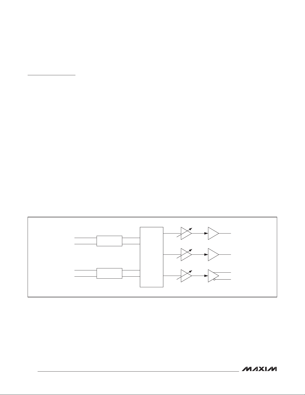
The MAX97002 signal path consists of flexible inputs,
signal mixing, volume control, and output amplifiers
2
C interface.
Signal Path
(Figure 2). The inputs can be configured for singleended or differential signals (Figure 3). The internal
preamplifiers feature programmable gain settings using
internal resistors and an external gain setting using a
trimmed internal feedback resistor. The external option
allows any desired gain to be selected. Following preamplification, the input signals are mixed, volume adjusted, and routed to the headphone and speaker amplifiers
based on the desired configuration.
Mixers
The MAX97002 features independent mixers for the left
headphone, right headphone, and speaker paths. Each
output can select any combination of any inputs. This
allows for mixing two audio signals together and routing independent signals to the headphone and speaker
amplifiers. If one of the inputs is not selected by either
mixer, it is automatically powered down to save power.
Class D Speaker Amplifier
The MAX97002 Class D speaker amplifier utilizes active
emissions limiting and spread-spectrum modulation to
minimize the EMI radiated by the amplifier.
Figure 2. Signal Path
18
INA2
INA1
INB2
INB1
INPUT A
-6dB TO +18dB
INPUT B
-6dB TO +18dB
MIXER
AND
MUX
-64dB TO +6dB
-64dB TO +6dB 0/3dB
-30dB TO +20dB +12dB
0/3dB
Page 19
Audio Subsystem with Mono Class D
Speaker and Class H Headphone Amplifiers
STEREO SINGLE-ENDED
IN_2 (R)
R
TO MIXER
IN_1 (L)
L
MAX97002
DIFFERENTIAL
IN_2 (+)
IN_1 (-)
Figure 3. Differential and Stereo Single-Ended Input Configurations
TO MIXER
19
Page 20
Audio Subsystem with Mono Class D
Speaker and Class H Headphone Amplifiers
Ultra-Low EMI Filterless Output Stage
Traditional Class D amplifiers require the use of external LC filters or shielding in order to meet EN55022B
electromagnetic-interference (EMI) regulation standards. Maxim’s active emissions limiting edge-rate
control circuitry and spread-spectrum modulation
reduces EMI emissions, while maintaining up to 87%
efficiency. Maxim’s spread-spectrum modulation
MAX97002
40
30
20
10
AMPLITUDE (dBµV/m)
0
-10
30 300
mode flattens wideband spectral components, while
proprietary techniques ensure that the cycle-to-cycle
variation of the switching period does not degrade audio
reproduction or efficiency. The MAX97002’s spreadspectrum modulator randomly varies the switching
frequency by Q20kHz around the center frequency
(250kHz). Above 10MHz, the wideband spectrum looks
like noise for EMI purposes (see Figure 4).
2802602402202001801601401201008060
FREQUENCY (MHz)
40
30
20
10
AMPLITUDE (dBµV/m)
0
-10
300 350 1000
Figure 4. EMI with 15cm of Speaker Cable
20
650
600550500450400
FREQUENCY (MHz)
950900850800750700
Page 21
Audio Subsystem with Mono Class D
Speaker and Class H Headphone Amplifiers
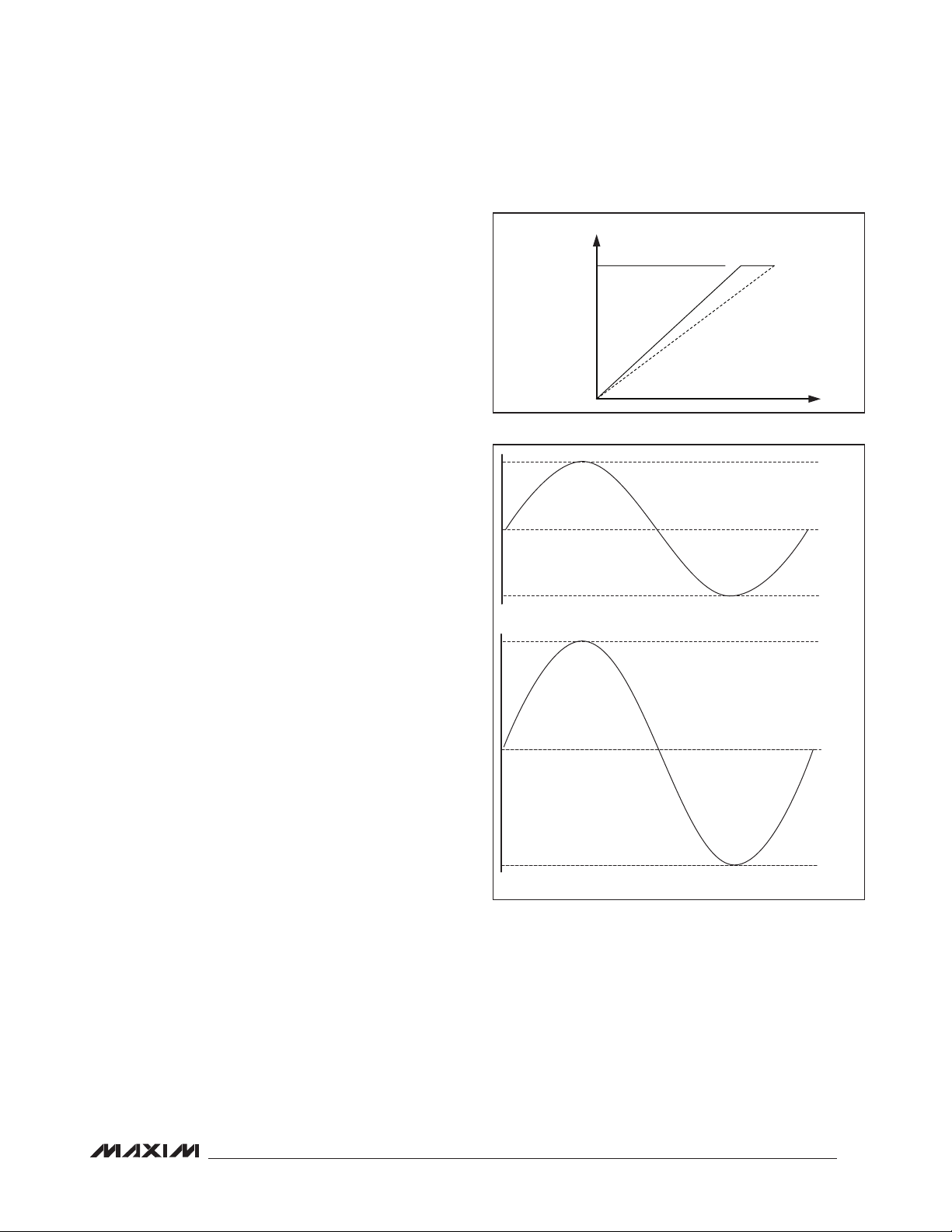
Distortion Limiter
The MAX97002 speaker amplifiers integrate a limiter
to provide speaker protection and audio compression.
When enabled, the limiter monitors the audio signal at
the output of the Class D speaker amplifier and decreases the gain if the distortion exceeds the predefined
threshold. The limiter automatically tracks the battery
voltage to reduce the gain as the battery voltage drops.
Figure 5 shows the typical output vs. input curves with
and without the distortion limiter. The dotted line shows
the maximum gain for a given distortion limit without
the distortion limiter. The solid line shows how, with the
distortion limiter enabled, the gain can be increased
without exceeding the set distortion limit. When the
limiter is enabled, selecting a high gain level results in
peak signals being attenuated while low signals are left
unchanged. This increases the perceived loudness without the harshness of a clipped waveform.
Analog Switch
The MAX97002 integrates a DPST analog audio switch
that connects COM1 and COM2 to OUTP and OUTN,
respectively. Unlike discrete solutions, the switch design
reduces coupling of Class D switching noise to the COM_
inputs. This eliminates the need for a costly T-switch.
Drive COM1 and COM2 with a low-impedance source
to minimize noise on the pins. In applications that do not
require the analog switch, leave COM1 and COM2 unconnected. When applying signal on COM1 and COM2, disable the Class D amplifier before closing the switch.
Headphone Amplifier
DirectDrive
Traditional single-supply headphone amplifiers have
outputs biased at a nominal DC voltage (typically half
the supply). Large coupling capacitors are needed to
block this DC bias from the headphone. Without these
capacitors, a significant amount of DC current flows to
the headphone, resulting in unnecessary power dissipation and possible damage to both headphone and
headphone amplifier.
®
Maxim’s DirectDrive
to create an internal negative supply voltage. This allows
the headphone outputs of the MAX97002 to be biased
at GND while operating from a single supply (Figure 6).
Without a DC component, there is no need for the large
DC-blocking capacitors. Instead of two large (220FF,
typ) capacitors, the MAX97002 charge pump requires
two small ceramic capacitors, conserving board space,
reducing cost, and improving the frequency response
of the headphone amplifier. See the Output Power
architecture uses a charge pump
V
OUT
MAXIMUM THD+N
LEVEL
V
IN
Figure 5. Limiter Gain Curve
V
DD
V
/ 2
DD
GND
CONVENTIONAL AMPLIFIER BIASING SCHEME
+V
DD
SGND
-V
DD
DirectDrive AMPLIFIER BIASING SCHEME
Figure 6.Traditional Amplifier Output vs. MAX97002
DirectDrive Output
vs. Load Resistance graph in the Typical Operating
Characteristics for details of the possible capacitor
sizes. There is a low DC voltage on the amplifier outputs due to amplifier offset. However, the offset of the
MAX97002 is typically Q0.6mV, which, when combined
with a 32I load, results in less than 50FA of DC current
flow to the headphones.
DirectDrive is a registered trademark of Maxim Integrated
Products, Inc.
MAX97002
21
Page 22
Audio Subsystem with Mono Class D
Speaker and Class H Headphone Amplifiers
In addition to the cost and size disadvantages of
the DC-blocking capacitors required by conventional
headphone amplifiers, these capacitors limit the amplifier’s low-frequency response and can distort the audio
signal. Previous attempts at eliminating the outputcoupling capacitors involved biasing the headphone
return (sleeve) to the DC-bias voltage of the headphone
amplifiers. This method raises some issues:
U The sleeve is typically grounded to the chassis. Using
MAX97002
the midrail biasing approach, the sleeve must be isolated from system ground, complicating product design.
U During an ESD strike, the amplifier’s ESD structures are
the only path to system ground. Thus, the amplifier must
be able to withstand the full energy from an ESD strike.
U When using the headphone jack as a line out to other
equipment, the bias voltage on the sleeve may conflict
with the ground potential from other equipment, resulting in possible damage to the amplifiers.
Charge Pump
The MAX97002’s dual-mode charge pump generates
both the positive and negative power supply for the
headphone amplifier. To maximize effficiency, both the
charge pump’s switching frequency and output voltage
change based on signal level.
When the input signal level is less than 10% of V
the switching frequency is reduced to a low rate. This
minimizes switching losses in the charge pump. When
the input signal exceeds 10% of V
, the switching fre-
DD
quency increases to support the load current.
For input signals below 25% of VDD, the charge pump
generates Q(V
/2) to minimize the voltage drop across
DD
the amplifier’s power stage and thus improves efficiency.
Input signals that exceed 25% of V
pump to output QV
. The higher output voltage allows
DD
cause the charge
DD
for full output power from the headphone amplifier.
To prevent audible glitches when transitioning from the
/2) output mode to the QVDD output mode, the
Q(V
DD
charge pump transitions very quickly. This quick change
draws significant current from V
transition. The bypass capacitor on V
required current and prevent droop on V
for the duration of the
DD
supplies the
DD
.
DD
DD
The charge pump’s dynamic switching mode can be
2
turned off through the I
can then be forced to output either Q(V
C interface. The charge pump
DD
regardless of input signal level.
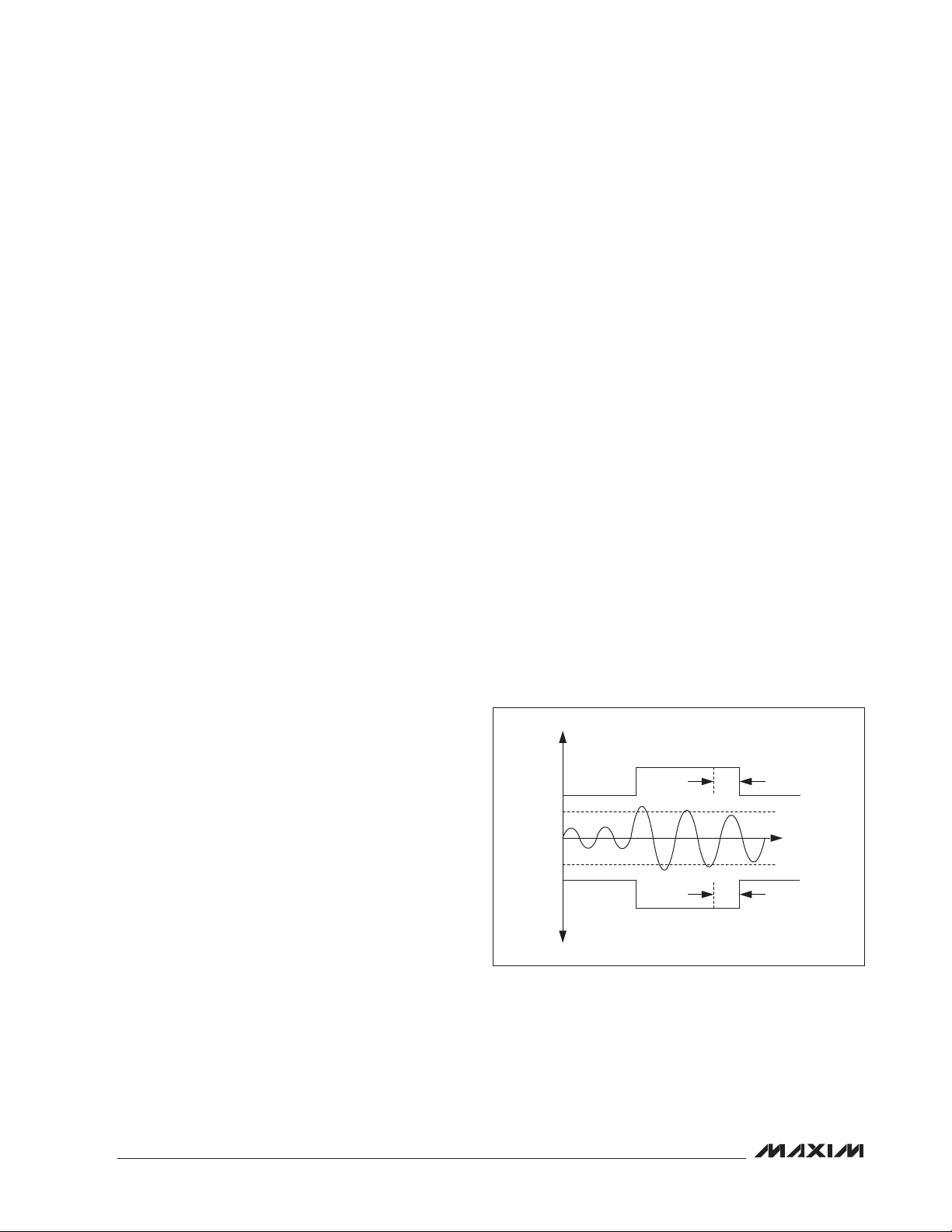
Class H Operation
A Class H amplifier uses a Class AB output stage with
power supplies that are modulated by the output signal.
In the case of the MAX97002, two nominal power-supply
differentials of 1.8V (+0.9V to -0.9V) and 3.6V (+1.8V
to -1.8V) are available from the charge pump. Figure 7
shows the operation of the output voltage dependent
power supply.
Low-Power Mode
To minimize power consumption when using the headphone amplifier, enable the low-power mode. In this
mode, the headphone mixers and volume control are
bypassed and shutdown.
I2C Slave Address
The MAX97002 uses a slave address of 0x9A or
1001101R/W. The address is defined as the 7 most significant bits (MSBs) followed by the read/write bit. Set the read/
write bit to 1 to configure the MAX97002 to read mode. Set
the read/write bit to 0 to configure the MAX97002 to write
mode. The address is the first byte of information sent to
the MAX97002 after the START (S) condition.
1.8V
HPVDD
0.9V
V
TH_H
V
TH_L
-0.9V
-1.8V
Figure 7. Class H Operation
HPVSS
32ms
32ms
/2) or QVDD
OUTPUT
VOLTAGE
22
Page 23
Audio Subsystem with Mono Class D
Speaker and Class H Headphone Amplifiers
I2C Registers
Nine internal registers program the MAX97002. Table 1
lists all of the registers, their addresses, and power-onreset states. Register 0xFF indicates the device revision.
Table 1. Register Map
REGISTER B7 B6 B5 B4 B3 B2 B1 B0 ADDRESS DEFAULT R/W
STATUS
Input Gain INADIFF INBDIFF PGAINA PGAINB 0x00 0x00 R/W
Headphone
Mixers
Speaker
Mixer
Headphone
Left
Headphone
Right
Speaker FFM SPKM SPKVOL 0x05 0x00 R/W
Reserved 0 0 0 0 0 0 0 0 0x06 0x00 R/W
Limiter THDCLP 0 0 0 THDT1 0x07 0x00 R/W
Power
Management
Charge Pump 0 0 0 0 0 0 CPSEL FIXED 0x09 0x00 R/W
REVISION ID
Rev ID REV 0xFF 0x00 R
0 0 0 0 SPKMIX 0x02 0x00 R/W
ZCD SLEW
HPGAIN 0 HPRM HPRVOL 0x04 0x00 R/W
SHDN
HPLMIX HPRMIX 0x01 0x00 R/W
HPLM HPLVOL 0x03 0x00 R/W
LPMODE SPKEN 0 HPLEN HPREN BYPEN 0x08 0x01 R/W
Write zeros to all unused bits in the register table when
updating the register, unless otherwise noted. Tables
2–7 describe each bit.
MAX97002
23
Page 24
Audio Subsystem with Mono Class D
Speaker and Class H Headphone Amplifiers
Table 2. Input Register
REGISTER BIT NAME DESCRIPTION
Input A Differential Mode. Configures the input A channel as either a mono differential
7 INADIFF
MAX97002
0x00
6 INBDIFF
5
4
3
2
1
0
PGAINA
PGAINB
signal (INA = INA2 - INA1) or as a stereo signal (INA1 = left, INA2 = right).
0 = Stereo single-ended
1 = Differential
Input B Differential Mode. Configures the input B channel as either a mono differential
signal (INB = INB2 - INB1) or as a stereo signal (INB1 = left, INB2 = right).
0 = Stereo single-ended
1 = Differential
Input A Preamp Gain. Set the input gain to maximize output signal level for a given input
signal range to improve the SNR of the system. PGAINA = 111 switches to a trimmed
20kI feedback resistor for external gain setting.
VALUE
000
001
010
011
100
101
110
111
Input B Preamp Gain. Set the input gain to maximize output signal level for a given input
signal range to improve the SNR of the system. PGAINB = 111 switches to a trimmed
20kI feedback resistor for external gain setting.
VALUE
000
001
010
011
100
101
110
111
LEVEL (dB)
-6
-3
0
3
6
9
18
External
LEVEL (dB)
-6
-3
0
3
6
9
18
External
24
Page 25
Audio Subsystem with Mono Class D
Speaker and Class H Headphone Amplifiers
Table 3. Mixer Registers
REGISTER BIT NAME DESCRIPTION
7
6
HPLMIX
5
4
0x01
3
2
HPRMIX
1
0
Left Headphone Mixer. Selects which of the four inputs is routed to the left headphone
output.
VALUE
0000
xxx1
xx1x
x1xx
1xxx
Right Headphone Mixer. Selects which of the four inputs is routed to the right
headphone output.
VALUE
0000
xxx1
xx1x
x1xx
1xxx
INPUT
No input
INA1 (disabled when INADIFF = 1)
INA2 (select when INADIFF = 1)
INB1 (disabled when INBDIFF = 1)
INB2 (select when INBDIFF = 1)
INPUT
No input
INA1 (disabled when INADIFF = 1)
INA2 (select when INADIFF = 1)
INB1 (disabled when INBDIFF = 1)
INB2 (select when INBDIFF = 1)
Mixers
MAX97002
0x02
3
2
SPKMIX
1
0
Speaker Mixer. Selects which of the four inputs is routed to the speaker output.
VALUE
0000
xxx1
xx1x
x1xx
1xxx
INPUT
No input
INA1 (disabled when INADIFF = 1)
INA2 (select when INADIFF = 1)
INB1 (disabled when INBDIFF = 1)
INB2 (select when INBDIFF = 1)
25
Page 26

Audio Subsystem with Mono Class D
Speaker and Class H Headphone Amplifiers
Volume Control
Table 4. Volume Control Registers
REGISTER BIT NAME DESCRIPTION
Zero-Crossing Detection. Determines whether zero-crossing detection is used on all vol-
ume control changes to reduce clicks and pops. Disabling zero-crossing detection allows
7
MAX97002
6
5 HPLM
4
0x03
3
2
1
0
ZCD
SLEW
HPLVOL
volume changes to occur immediately.
0 = Enabled
1 = Disabled
Volume Slewing. Determines whether volume slewing is used on all volume control changes to reduce clicks and pops. When enabled, volume changes cause the
MAX97002 to ramp through intermediate volume settings whenever a change to the
volume is made. If ZCD = 1, slewing occurs at a rate of 0.2ms per step. If ZCD = 0, slew
time depends on the input signal. Write a 1 to this bit to disable slewing and implement
volume changes immediately. This bit also activates soft-start at power-on and soft-stop
and power-off.
0 = Enabled
1 = Disabled
Left Headphone Mute
0 = Unmuted
1 = Muted
Left Headphone Volume
VALUE LEVEL (dB) VALUE LEVEL (dB)
0x00 -64 0x10 -12
0x01 -60dB 0x11 -10
0x02 -56 0x12 -8
0x03 -52 0x13 -6
0x04 -48 0x14 -4
0x05 -44 0x15 -2
0x06 -40 0x16 -1
0x07 -37 0x17 0
0x08 -34 0x18 1
0x09 -31 0x19 2
0x0A -28 0x1A 3
0x0B -25 0x1B 4
0x0C -22 0x1C 4.5
0x0D -19 0x1D 5
0x0E -16 0x1E 5.5
0x0F -14 0x1F 6
26
Page 27

Audio Subsystem with Mono Class D
Speaker and Class H Headphone Amplifiers
Table 4. Volume Control Registers (continued)
REGISTER BIT NAME DESCRIPTION
Headphone Gain. Controls the headphone amplifier gain.
7 HPGAIN
5 HPRM
4
3
0x04
2
HPRVOL
1
0
0 = 0dB
1 = 3dB
Right Headphone Mute
0 = Unmuted
1 = Muted
Right Headphone Volume
VALUE LEVEL (dB) VALUE LEVEL (dB)
0x00 -64 0x10 -12
0x01 -60dB 0x11 -10
0x02 -56 0x12 -8
0x03 -52 0x13 -6
0x04 -48 0x14 -4
0x05 -44 0x15 -2
0x06 -40 0x16 -1
0x07 -37 0x17 0
0x08 -34 0x18 1
0x09 -31 0x19 2
0x0A -28 0x1A 3
0x0B -25 0x1B 4
0x0C -22 0x1C 4.5
0x0D -19 0x1D 5
0x0E -16 0x1E 5.5
0x0F -14 0x1F 6
MAX97002
27
Page 28

Audio Subsystem with Mono Class D
Speaker and Class H Headphone Amplifiers
Table 4. Volume Control Registers (continued)
REGISTER BIT NAME DESCRIPTION
Fixed-Frequency Oscillation. Removes spread spectrum from the Class D oscillator.
7 FFM
6 SPKM
MAX97002
5
4
0x05
3
2
1
0 0x25 2 0x33 14
SPKVOL
0 = Spread-spectrum mode
1 = Fixed-frequency mode
Speaker Mute
0 = Unmuted
1 = Mute
Speaker Volume
VALUE LEVEL (dB) VALUE LEVEL (dB) VALUE
0x00–0x18 -30 0x26 3 0x34 14.5
0x19 -26 0x27 4 0x35 15
0x1A -22 0x28 5 0x36 15.5
0x1B -18 0x29 6 0x37 16
0x1C -14 0x2A 7 0x38 16.5
0x1D -12 0x2B 8 0x39 17
0x1E -10 0x2C 9 0x3A 17.5
0x1F -8 0x2D 10 0x3B 18
0x20 -6 0x2E 11 0x3C 18.5
0x21 -4 0x2F 12 0x3D 19
0x22 -2 0x30 12.5 0x3E 19.5
0x23 0 0x31 13 0x3F 20
0x24 1 0x32 13.5
LEVEL
(dB)
28
Page 29

Audio Subsystem with Mono Class D
Speaker and Class H Headphone Amplifiers
Table 5. Distortion Limiter Register
REGISTER BIT NAME DESCRIPTION
Distortion Limit
VALUE THD LIMIT (%)
0000 Disabled
0001–1001
1010
1011
1100
1101
1110
1111
0000 Disabled
Distortion Release Time Constant
0 = 1.4s
1 = 2.8s
0x07
7
6
THDCLP
5
4
0 THDT1
Distortion Limiter
MAX97002
P 4
P 5
P 6
P 8
P 11
P 12
P 15
Power Management
Table 6. Power Management Register
REGISTER BIT NAME DESCRIPTION
Software Shutdown
0 = Device disabled
1 = Device enabled
Low-Power Headphone Mode. Enables low-power headphone mode. When activated this
mode directly connects the selected channel to the headphone amplifiers, bypassing the
mixers and the volume control. Additionally, low-power mode disables the speaker path.
VALUE LIMIT
00 Disabled
01 INA (SE) Connected to the headphone output
10 INB (SE) Connected to the headphone output
11 INA (Diff) to HPL and INB (Diff) to HPR
Speaker Amplifier Enable
0 = Disabled
1 = Enabled
Left Headphone Amplifier Enable
0 = Disabled
1 = Enabled
Right Headphone Amplifier Enable
0 = Disabled
1 = Enabled
Analog Switch
0 = Open
1 = Closed
0x08
7
6
5
4 SPKEN
2 HPLEN
1 HPREN
0 BYPEN
SHDN
LPMODE
29
Page 30

Audio Subsystem with Mono Class D
Speaker and Class H Headphone Amplifiers
Charge-Pump Control
Table 7. Charge-Pump Control Register
REGISTER BIT NAME DESCRIPTION
Charge-Pump Output Select. Works with the FIXED to set Q1.8V or Q0.9V outputs on
1 CPSEL
MAX97002
0x09
0 FIXED
HPVDD and HPVSS. Ignored when FIXED = 0.
0 = Q1.8V on HPVDD/HPVSS
1 = Q0.9V on HPVDD/HPVSS
Class H Mode. When enabled, this bit forces the charge pump to generate static power
rails for HPVDD and HPVSS, instead of dynamically adjusting them based on output signal level.
0 = Class H mode
1 = Fixed-supply mode
I2C Serial Interface
The MAX97002 features an I2C/SMBusK-compatible,
2-wire serial interface consisting of a serial-data line
(SDA) and a serial-clock line (SCL). SDA and SCL facilitate communication between the MAX97002 and the
master at clock rates up to 400kHz. Figure 1 shows the
2-wire interface timing diagram. The master generates
SCL and initiates data transfer on the bus. The master
device writes data to the MAX97002 by transmitting the
proper slave address followed by the register address
and then the data word. Each transmit sequence is
framed by a START (S) or REPEATED START (Sr) condition and a STOP (P) condition. Each word transmitted
to the MAX97002 is 8 bits long and is followed by an
acknowledge clock pulse. A master reading data from
the MAX97002 transmits the proper slave address followed by a series of nine SCL pulses. The MAX97002
transmits data on SDA in sync with the master-generated
SCL pulses. The master acknowledges receipt of each
byte of data. Each read sequence is framed by a START
or REPEATED START condition, a not acknowledge,
and a STOP condition. SDA operates as both an input
and an open-drain output. A pullup resistor, typically
greater than 500I, is required on SDA. SCL operates
only as an input. A pullup resistor, typically greater than
500I, is required on SCL if there are multiple masters on
the bus, or if the single master has an open-drain SCL
output. Series resistors in line with SDA and SCL are
optional. Series resistors protect the digital inputs of the
MAX97002 from high voltage spikes on the bus lines and
minimize crosstalk and undershoot of the bus signals.
Bit Transfer
One data bit is transferred during each SCL cycle. The data
on SDA must remain stable during the high period of the
SCL pulse. Changes in SDA while SCL is high are control
signals (see the START and STOP Conditions section).
START and STOP Conditions
SDA and SCL idle high when the bus is not in use. A
master initiates communication by issuing a START condition. A START condition is a high-to-low transition on
SDA with SCL high. A STOP condition is a low-to-high
transition on SDA while SCL is high (Figure 8). A START
condition from the master signals the beginning of a
transmission to the MAX97002. The master terminates
transmission, and frees the bus, by issuing a STOP condition. The bus remains active if a REPEATED START
condition is generated instead of a STOP condition.
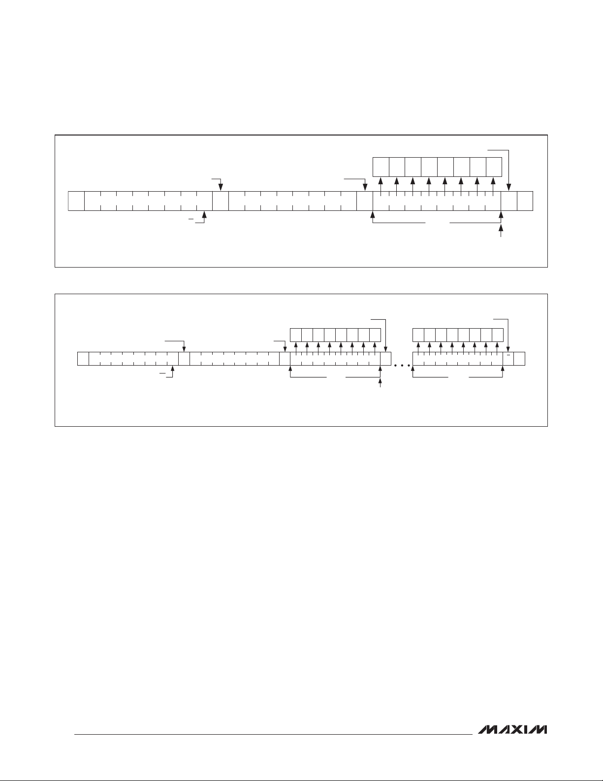
S Sr P
SCL
SDA
Figure 8. START, STOP, and REPEATED START Conditions
SMBus is a trademark of Intel Corp.
30
Page 31

Audio Subsystem with Mono Class D
Speaker and Class H Headphone Amplifiers
Early STOP Conditions
The MAX97002 recognizes a STOP (P) condition at any
point during data transmission except if the STOP condition occurs in the same high pulse as a START (S) condition. For proper operation, do not send a STOP condition
during the same SCL high pulse as the START condition.
Slave Address
The slave address is defined as the seven most significant bits (MSBs) followed by the read/write bit. For
the MAX97002 the 7 MSBs are 1001101. Setting the
read/write bit to 1 (slave address = 0x9B) configures the
MAX97002 for read mode. Setting the read/write bit to 0
(slave address = 0x9A) configures the MAX97002 for write
mode. The address is the first byte of information sent to
the MAX97002 after the START condition.
Acknowledge
The acknowledge bit (ACK) is a clocked 9th bit that
the MAX97002 uses to handshake receipt each byte
of data when in write mode (Figure 9). The MAX97002
pulls down SDA during the entire master-generated 9th
clock pulse if the previous byte is successfully received.
Monitoring ACK allows for detection of unsuccessful
data transfers. An unsuccessful data transfer occurs
if a receiving device is busy or if a system fault has
occurred. In the event of an unsuccessful data transfer,
the bus master retries communication. The master pulls
down SDA during the 9th clock cycle to acknowledge
receipt of data when the MAX97002 is in read mode. An
acknowledge is sent by the master after each read byte
to allow data transfer to continue. A not-acknowledge is
sent when the master reads the final byte of data from
MAX97002
the MAX97002, followed by a STOP condition.
Write Data Format
A write to the MAX97002 includes transmission of a
START condition, the slave address with the R/W bit set
to 0, one byte of data to configure the internal register
address pointer, one or more bytes of data, and a STOP
condition. Figure 10 illustrates the proper frame format
for writing one byte of data to the MAX97002. Figure 11
illustrates the frame format for writing n-bytes of data to
the MAX97002.
The slave address with the R/W bit set to 0 indicates that
the master intends to write data to the MAX97002. The
MAX97002 acknowledges receipt of the address byte
during the master-generated 9th SCL pulse.
The second byte transmitted from the master configures
the MAX97002’s internal register address pointer. The
pointer tells the MAX97002 where to write the next byte
of data. An acknowledge pulse is sent by the MAX97002
upon receipt of the address pointer data.
The third byte sent to the MAX97002 contains the
data that is written to the chosen register. An acknowledge pulse from the MAX97002 signals receipt of the
data byte. The address pointer autoincrements to the
next register address after each received data byte.
This autoincrement feature allows a master to write to
sequential registers within one continuous frame. The
master signals the end of transmission by issuing a
STOP condition. Register addresses greater than 0x09
are reserved. Do not write to these addresses.
Figure 9. Acknowledge
CONDITION
SCL
SDA
START
28 9
1
CLOCK PULSE FOR
ACKNOWLEDGMENT
NOT ACKNOWLEDGE
ACKNOWLEDGE
31
Page 32
Audio Subsystem with Mono Class D
Speaker and Class H Headphone Amplifiers
ACKNOWLEDGE FROM MAX97002
B1 B0B3 B2B5 B4B7 B6
ACKNOWLEDGE FROM MAX97002
S AA
0SLAVE ADDRESS REGISTER ADDRESS
ACKNOWLEDGE FROM MAX97002
DATA BYTE
A
P
R/W
MAX97002
Figure 10. Writing One Byte of Data to the MAX97002
ACKNOWLEDGE FROM MAX97002
S
SLAVE ADDRESS
R/W
Figure 11. Writing n-Bytes of Data to the MAX97002
Send the slave address with the R/W bit set to 1 to initiate
a read operation. The MAX97002 acknowledges receipt
of its slave address by pulling SDA low during the 9th
SCL clock pulse. A START (S) command followed by
a read command resets the address pointer to register
0x00.
The first byte transmitted from the MAX97002 is the contents of register 0x00. Transmitted data is valid on the
rising edge of SCL. The address pointer autoincrements
after each read data byte. This autoincrement feature
allows all registers to be read sequentially within one
continuous frame. A STOP condition can be issued after
any number of read data bytes. If a STOP (P) condition is
issued followed by another read operation, the first data
byte to be read is from register 0x00.
ACKNOWLEDGE FROM MAX97002
A
REGISTER ADDRESS
Read Data Format
ACKNOWLEDGE FROM MAX97002
B1 B0B3 B2B5 B4B7 B6
A
DATA BYTE 1
1 BYTE
AUTOINCREMENT INTERNAL
REGISTER ADDRESS POINTER
The address pointer can be preset to a specific register
before a read command is issued. The master presets
the address pointer by first sending the MAX97002’s
slave address with the R/W bit set to 0 followed by the
register address. A REPEATED START (Sr) condition is
then sent followed by the slave address with the R/W bit
set to 1. The MAX97002 then transmits the contents of
the specified register. The address pointer autoincrements after transmitting the first byte.
The master acknowledges receipt of each read byte
during the acknowledge clock pulse. The master must
acknowledge all correctly received bytes except the last
byte. The final byte must be followed by a not acknowledge from the master and then a STOP condition. Figure
12 illustrates the frame format for reading one byte from
the MAX97002. Figure 13 illustrates the frame format for
reading multiple bytes from the MAX97002.
1 BYTE
ACKNOWLEDGE FROM MAX97002
A0
AUTOINCREMENT INTERNAL
REGISTER ADDRESS POINTER
B1 B0B3 B2B5 B4B7 B6
DATA BYTE n
1 BYTE
P
A
32
Page 33
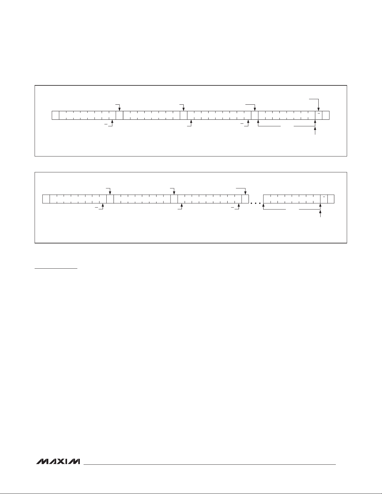
Audio Subsystem with Mono Class D
Speaker and Class H Headphone Amplifiers
MAX97002
ACKNOWLEDGE FROM MAX97002
S
R/W
Figure 12. Reading One Byte of Data from the MAX97002
ACKNOWLEDGE FROM MAX97002
S
Figure 13. Reading n-Bytes of Data from the MAX97002
0
R/W
ACKNOWLEDGE FROM MAX97002
0
ACKNOWLEDGE FROM MAX97002
Sr 1SLAVE ADDRESS REGISTER ADDRESS SLAVE ADDRESS DATA BYTE
REPEATED START
Applications Information
Filterless Class D Operation
Traditional Class D amplifiers require an output filter to
recover the audio signal from the amplifier’s output. The
filters add cost, increase the solution size of the amplifier,
and can decrease efficiency and THD+N performance.
The traditional PWM scheme uses large differential output swings (2 x V
DD(P-P)
rents. Any parasitic resistance in the filter components
results in a loss of power, lowering the efficiency.
The MAX97002 does not require an output filter. The
device relies on the inherent inductance of the speaker
coil and the natural filtering of both the speaker and
the human ear to recover the audio component of the
square-wave output. Eliminating the output filter results
in a smaller, less costly, more efficient solution.
Because the frequency of the MAX97002 output is well
beyond the bandwidth of most speakers, voice coil
movement due to the square-wave frequency is very
small. Although this movement is small, a speaker not
designed to handle the additional power can be damaged. For optimum results, use a speaker with a series
inductance > 10FH. Typical 8I speakers exhibit series
inductances in the 20FH to 100FH range.
) and causes large ripple cur-
ACKNOWLEDGE FROM MAX97002
Sr 1SLAVE ADDRESS REGISTER ADDRESS SLAVE ADDRESS DATA BYTE
ACKNOWLEDGE FROM MAX97002
R/W
NOT ACKNOWLEDGE FROM MASTER
AA
R/WREPEATED START
AA
1 BYTE
AUTOINCREMENT INTERNAL
REGISTER ADDRESS POINTER
1 BYTE
AUTOINCREMENT INTERNAL
REGISTER ADDRESS POINTER
RF Susceptibility
GSM radios transmit using time-division multiple access
(TDMA) with 217Hz intervals. The result is an RF signal
with strong amplitude modulation at 217Hz and its harmonics that are easily demodulated by audio amplifiers.
The MAX97002 is designed specifically to reject RF
signals; however, PCB layout has a large impact on the
susceptibility of the end product.
In RF applications, improvements to both layout and
component selection decreases the MAX97002’s susceptibility to RF noise and prevent RF signals from being
demodulated into audible noise. Trace lengths should
be kept below 1/4 of the wavelength of the RF frequency
of interest. Minimizing the trace lengths prevents them
from functioning as antennas and coupling RF signals
into the MAX97002. The wavelength (l) in meters is
given by:
l = c/f
8
where c = 3 x 10
m/s, and f = the RF frequency of
interest.
Route the audio signals on the middle layers of the PCB
to allow the ground planes above and below to shield
them from RF interference. Ideally, the top and bottom
layers of the PCB should primarily be ground planes to
create effective shielding.
P
A
A P
33
Page 34
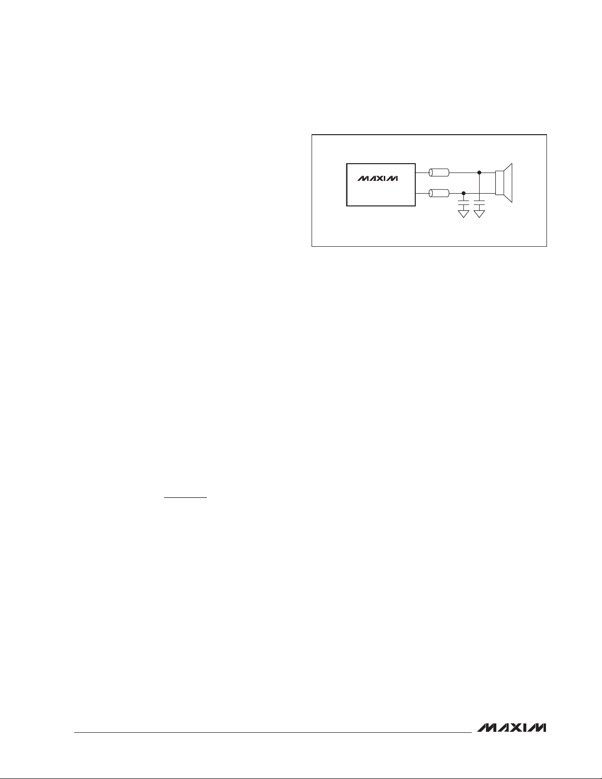
Audio Subsystem with Mono Class D
Speaker and Class H Headphone Amplifiers
Additional RF immunity can also be obtained from relying on the self-resonant frequency of capacitors as it
exhibits the frequency response similar to a notch filter.
Depending on the manufacturer, 10pF to 20pF capacitors
typically exhibit self resonance at RF frequencies. These
capacitors when placed at the input pins can effectively
shunt the RF noise at the inputs of the MAX97002. For
these capacitors to be effective, they must have a lowimpedance, low-inductance path to the ground plane.
MAX97002
Do not use microvias to connect to the ground plane as
these vias do not conduct well at RF frequencies.
Component Selection
Optional Ferrite Bead Filter
Additional EMI suppression can be achieved using a
filter constructed from a ferrite bead and a capacitor to
ground (Figure 14). Use a ferrite bead with low DC resistance, high-frequency (> 600MHz) impedance between
100I and 600I, and rated for at least 1A. The capacitor
value varies based on the ferrite bead chosen and the
actual speaker lead length. Select a capacitor less than
1nF based on EMI performance.
Input Capacitor
An input capacitor, C
impedance of the MAX97002 line inputs forms a highpass filter that removes the DC bias from an incoming
analog signal. The AC-coupling capacitor allows the
amplifier to automatically bias the signal to an optimum
DC level. Assuming zero-source impedance, the -3dB
point of the highpass filter is given by:
Choose CIN such that f
quency of interest. For best audio quality, use capacitors
whose dielectrics have low-voltage coefficients, such as
tantalum or aluminum electrolytic. Capacitors with highvoltage coefficients, such as ceramics, may result in
increased distortion at low frequencies.
Use capacitors with an ESR less than 100mI for optimum
performance. Low-ESR ceramic capacitors minimize the
output resistance of the charge pump. Most surfacemount ceramic capacitors satisfy the ESR requirement.
For best performance over the extended temperature
range, select capacitors with an X7R dielectric.
, in conjunction with the input
IN
1
=
f
−
3dB
Charge-Pump Capacitor Selection
π
2 R C
IN IN
is well below the lowest fre-
-3dB
MAX97002
Figure 14. Optional Class D Ferrite Bead Filter
The value of the flying capacitor (connected between
C1N and C1P) affects the output resistance of the
charge pump. A value that is too small degrades the
device’s ability to provide sufficient current drive, which
leads to a loss of output voltage. Increasing the value
of the flying capacitor reduces the charge-pump output
resistance to an extent. Above 1FF, the on-resistance
of the internal switches and the ESR of external chargepump capacitors dominate.
The holding capacitor (bypassing HPVDD and HPVSS)
value and ESR directly affect the ripple on the supply.
Increasing the capacitor’s value reduces output ripple.
Likewise, decreasing the ESR reduces both ripple and
output resistance. Lower capacitance values can be
used in systems with low maximum output power levels.
See the Output Power vs. Load Resistance graph in the
Typical Operating Characteristics for more information
Supply Bypassing, Layout, and Grounding
Proper layout and grounding are essential for optimum performance. Use a large continuous ground
plane on a dedicated layer of the PCB to minimize
loop areas. Connect GND directly to the ground plane
using the shortest trace length possible. Proper grounding improves audio performance, minimizes crosstalk
between channels, and prevents any digital noise from
coupling into the analog audio signals.
Place the capacitor between C1P and C1N as close
to the MAX97002 as possible to minimize trace length
from C1P to C1N. Inductance and resistance added
between C1P and C1N reduce the output power of the
headphone amplifier. Bypass HPVDD and HPVSS with
capacitors located close to the pins with a short trace
length to GND. Close decoupling of HPVDD and HPVSS
minimizes supply ripple and maximizes output power
from the headphone amplifier.
OUT+
OUT-
Charge-Pump Flying Capacitor
Charge-Pump Holding Capacitor
34
Page 35
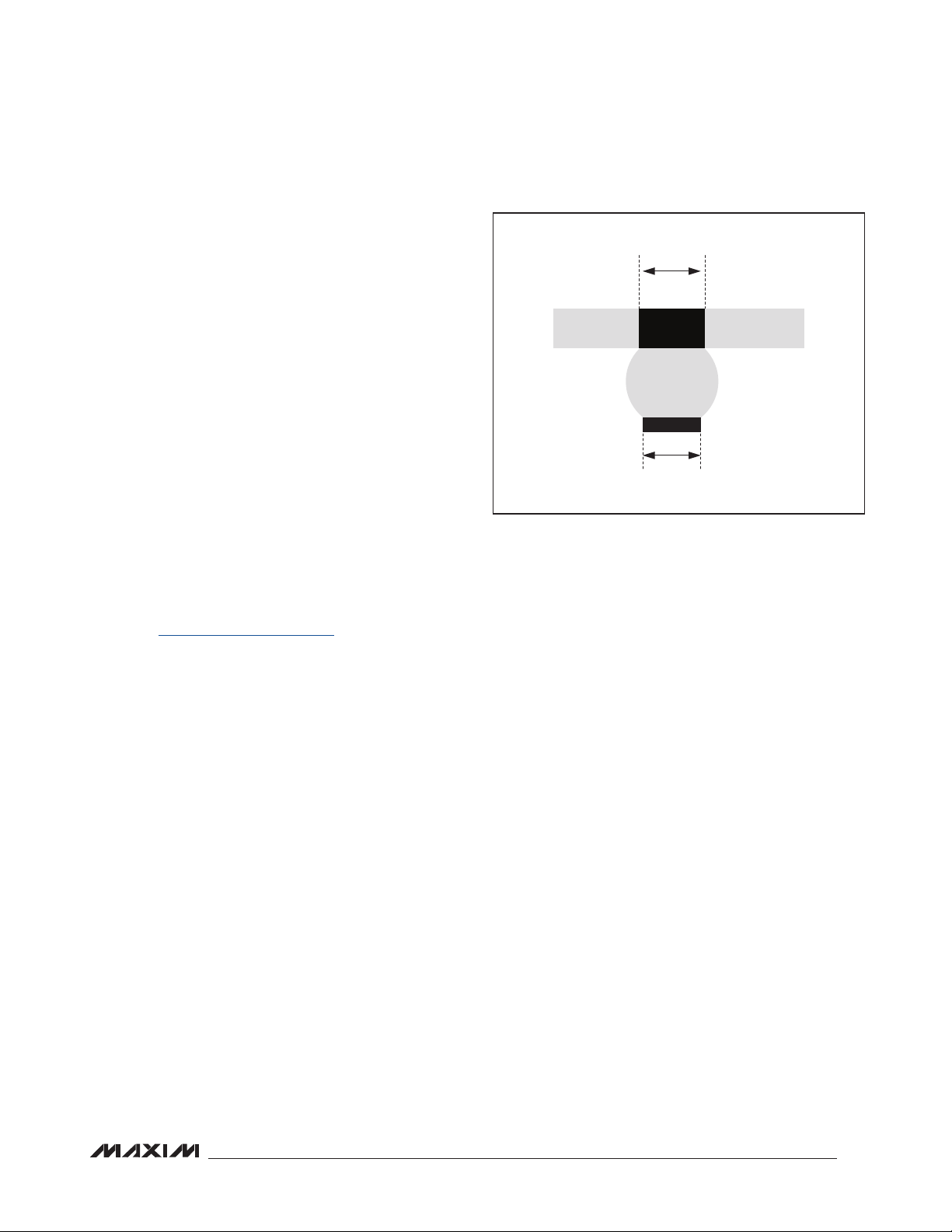
Audio Subsystem with Mono Class D
Speaker and Class H Headphone Amplifiers
Bypass PVDD to GND with as little trace length as possible. Connect OUTP and OUTN to the speaker using
the shortest and widest traces possible. Reducing trace
length minimizes radiated EMI. Route OUTP/OUTN as
a differential pair on the PCB to minimize the loop area,
thereby reducing the inductance of the circuit. If filter
components are used on the speaker outputs, be sure
to locate them as close as possible to the MAX97002
to ensure maximum effectiveness. Minimize the trace
length from any ground tied passive components to
GND to further minimize radiated EMI.
An evaluation kit (EV kit) is available to provide an
example layout for the MAX97002. The EV kit allows
quick setup of the MAX97002 and includes easy-to-use
software, allowing all internal registers to be controlled.
WLP Applications Information
For the latest application details on WLP construction,
dimensions, tape carrier information, PCB techniques,
bump-pad layout, and the recommended reflow temperature profile, as well as the latest information on reliability
testing results, refer to the Application Note 1891: Wafer-
Level Packaging (WLP) and Its Applications on Maxim’s
website at www.maxim-ic.com/ucsp. See Figure 15 for
the recommended PCB footprint for the MAX97002.
MAX97002
0.25mm
0.22mm
Figure 15. Recommended PCB Footprint
35
Page 36
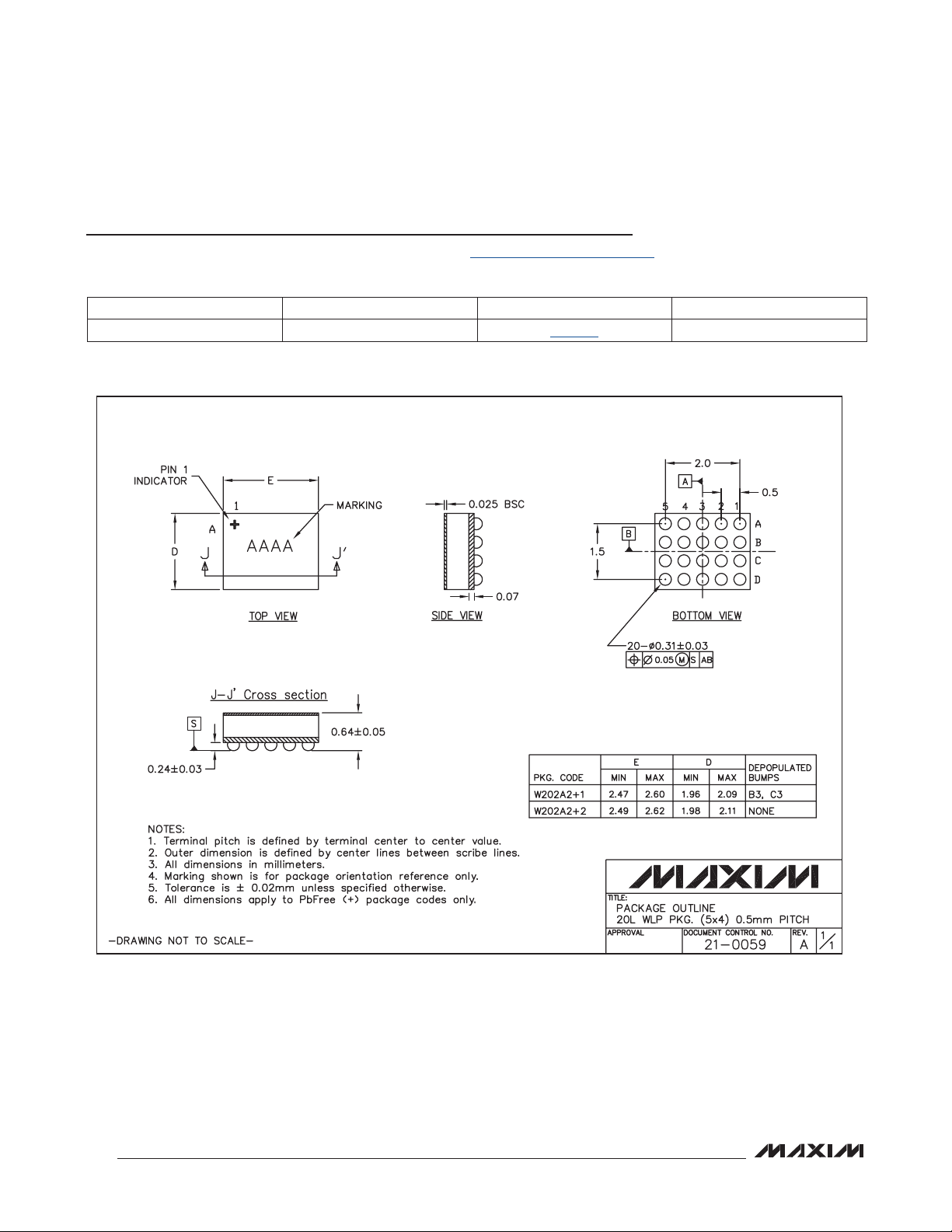
Audio Subsystem with Mono Class D
Speaker and Class H Headphone Amplifiers
Package Information
For the latest package outline information and land patterns, go to www.maxim-ic.com/packages. Note that a “+”, “#”, or “-” in the
package code indicates RoHS status only. Package drawings may show a different suffix character, but the drawing
pertains to the package regardless of RoHS status.
PACKAGE TYPE PACKAGE CODE OUTLINE NO. LAND PATTERN NO.
20 WLP W202A2+2
21-0059
—
MAX97002
20L WLP.EPS
36
Page 37
Audio Subsystem with Mono Class D
Speaker and Class H Headphone Amplifiers
Revision History
MAX97002
REVISION
NUMBER
0 1/10 Initial release —
1 7/10 Corrected mixer bit descriptions 25
REVISION
DATE
DESCRIPTION
PAGES
CHANGED
Maxim cannot assume responsibility for use of any circuitry other than circuitry entirely embodied in a Maxim product. No circuit patent licenses are implied.
Maxim reserves the right to change the circuitry and specifications without notice at any time.
Maxim Integrated Products, 120 San Gabriel Drive, Sunnyvale, CA 94086 408-737-7600 37
©
2010 Maxim Integrated Products Maxim is a registered trademark of Maxim Integrated Products, Inc.
 Loading...