

Page 1
General Description
The MAX9691/MAX9692/MAX9693 are ultra-fast ECL
comparators capable of very short propagation delays.
Their design maintains the excellent DC matching characteristics normally found only in slower comparators.
The MAX9691/MAX9692/MAX9693 have differential
inputs and complementary outputs that are fully compatible with ECL-logic levels. Output current levels are
capable of driving 50Ω terminated transmission lines.
The ultra-fast operation makes signal processing possible at frequencies in excess of 600MHz.
The MAX9692/MAX9693 feature a latch-enable (LE)
function that allows the comparator to be used in a
sample-hold mode. When LE is ECL high, the comparator functions normally. When LE is driven ECL low, the
outputs are forced to an unambiguous ECL-logic state,
dependent on the input conditions at the time of the
latch input transition. If the latch-enable function is not
used on either of the two comparators, the appropriate
LE input must be connected to ground; the companion
LE input must be connected to a high ECL logic level.
These devices are available in SO, QSOP, and tiny
µMAX®packages for added space savings.
________________________Applications
High-Speed Line Receivers
Peak Detectors
Threshold Detectors
High-Speed Triggers
Features
o 1.2ns Propagation Delay
o 100ps Propagation Delay Skew
o 150ps Dispersion
o 0.5ns Latch Setup Time
o 0.5ns Latch-Enable Pulse Width
o Available in µMAX and QSOP Packages
o +5V, -5.2V Power Supplies
MAX9691/MAX9692/MAX9693
Single/Dual, Ultra-Fast, ECL-Output
Comparators with Latch Enable
________________________________________________________________
Maxim Integrated Products
1
_________________________________________________________
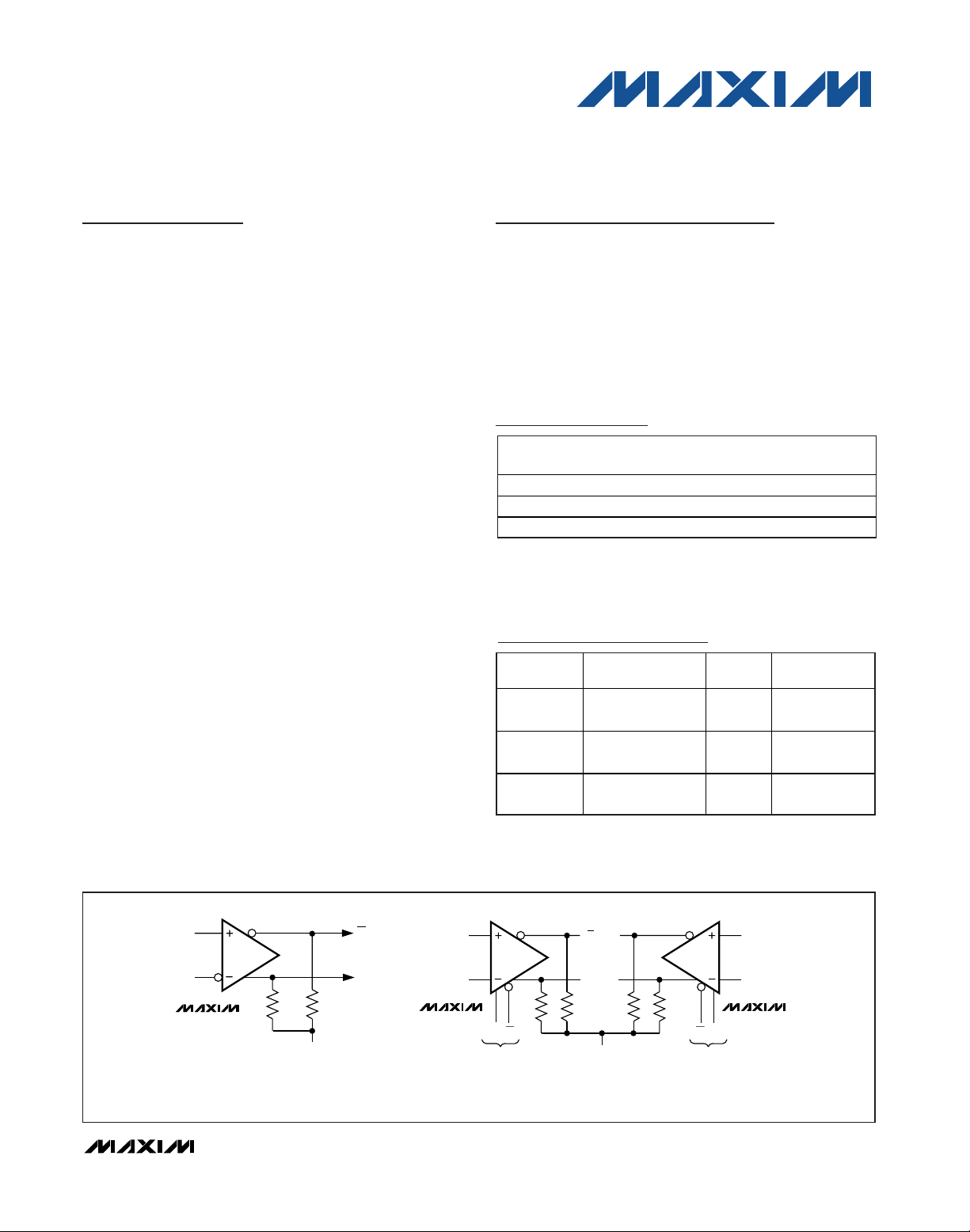
Functional Diagrams
19-1789; Rev 2; 1/12
Ordering Information
Ordering Information continued at the end of data sheet.
Pin Configurations appear at end of data sheet.
Selector Guide
For pricing, delivery, and ordering information, please contact Maxim Direct at 1-888-629-4642,
or visit Maxim’s website at www.maxim-ic.com.
Note: Devices are also available in lead(Pb)-free/RoHS-compli-
ant packages. Specify lead-free by adding a “+” after the part
number.
µMAX is a registered trademark of Maxim Integrated Products, Inc.
PART
MAX9691EUA -40°C to +85°C 8 µMAX
MAX9691ESA -40°C to +85°C 8 SO
MAX9691EPA -40°C to +85°C 8 PDIP
TEMP
RANGE
PIN-PACKAGE
PART
MAX9691 1 No
MAX9692 1 Yes
MAX9693 2 Yes
COMPARATORS
PER PACKAGE
LATCH
ENABLE
PINPACKAGE
8 µMAX,
8 SO, 8 PDIP
10 µMAX,
16 SO, 16 PDIP
16 QSOP,
16 SO, 16 PDIP
NONINVERTING
IN+
IN-
R
R
L
MAX9691
L
V
Q OUT
Q OUT
T
THE OUTPUTS ARE OPEN EMITTERS, REQUIRING EXTERNAL PULLDOWN
RESISTORS. THESE RESISTORS MAY BE IN THE RANGE OF 50Ω TO 200Ω
CONNECTED TO -2.0V, OR 240Ω TO 2000Ω CONNECTED TO -5.2V.
INPUT
INVERTING
INPUT
R
MAX9693 MAX9693
LATCH ENABLE
L
LE LE
R
Q OUT
L
Q OUT
V
T
NONINVERTING
INPUT
INVERTING
INPUT
R
L
R
L
LE LE
LATCH ENABLE
Page 2
MAX9691/MAX9692/MAX9693
Single/Dual, Ultra-Fast, ECL-Output
Comparators with Latch Enable
2 _______________________________________________________________________________________
ABSOLUTE MAXIMUM RATINGS
ELECTRICAL CHARACTERISTICS
(VCC= +5V, VEE= -5.2V, RL= 50Ω to VT, VT= -2V, LE = 0, TA= T
MIN
to T
MAX
, unless otherwise noted.)
Stresses beyond those listed under “Absolute Maximum Ratings” may cause permanent damage to the device. These are stress ratings only, and functional
operation of the device at these or any other conditions beyond those indicated in the operational sections of the specifications is not implied. Exposure to
absolute maximum rating conditions for extended periods may affect device reliability.
Supply Voltage (VCC) ...............................................-0.3V to +6V
Supply Voltage (VEE)................................................-6V to +0.3V
Input Voltage....................................(VCC+ 0.3V) to (VEE- 0.3V)
Output Short-Circuit Duration ....................................Continuous
Differential Input Voltage ......................................................±5V
Latch Enable ...............................................(V
EE
- 0.3V) to +0.3V
Output Current ....................................................................50mA
Input Current ....................................................................±25mA
Continuous Power Dissipation (TA= +70°C)
8-Pin µMAX (derate 4.8mW/°C above 70°C)...............387.8mW
8-Pin SO (derate 7.4mW/°C above +70°C)..................588.2mW
8-Pin PDIP (derate 9.1mW/°C above +70°C) ...........727.3mW
10-Pin µMAX (derate 8.8mW/°C above +70°C) ...........707.3mW
16-Pin QSOP (derate 9.6mW/°C above +70°C) .........771.5mW
16-Pin SO (derate 13.3mW/°C above +70°C) ..........1066.7mW
16-Pin PDIP (derate 10.5mW/°C above +70°C) .......842.1mW
Operating Temperature Range ...........................-40°C to +85°C
Junction Temperature......................................................+150°C
Storage Temperature Range .............................-55°C to +150°C
Lead Temperature (soldering, 10s) .................................+300°C
Soldering Temperature (reflow) .......................................+260°C
)
)
PARAMETER SYMBOL CONDITIONS MIN TYP MAX UNITS
Input Offset Voltage V
OS
Temperature Coefficient ∆VOS/∆T 10 µV/°C
Input Offset Current I
Input Bias Current I
Input Voltage Range V
OS
B
CM
Common-Mode Rejection Ratio CMRR -2.5V ≤ VCM ≤ +3.0V (Note 1) 60 80 dB
Positive Power-Supply Rejection
Ratio
Negative Power-Supply
Rejection Ratio
+PSRR 4.5V ≤ V
-PSRR -5.7V ≤ V
Open-Loop Gain AOL VCM = 0V 70 dB
Differential Input Resistance R
Differential Input Clamp Voltage 1.7 V
Input Capacitance C
Latch Enable Input Current High I
Latch Enable Input Current Low I
Latch E nab l e Log i c H i g h V ol tag eV
Latch Enable Logic Low Voltage V
Logic Output Low Voltage V
IH(LE)
IL(LE)
IH(LE
IL(LE
OH
OL
TA = +25°C -6.5 6.5
T
= T
A
to T
MIN
MAX
TA = +25°C 0.2 5
T
= T
A
to T
MIN
MAX
TA = +25°C620
T
= T
A
to T
MIN
MAX
Note 1 -2.5 +3.0 V
≤ 5.5V 60 dB
CC
≤ -4.7V 60 dB
EE
IN
IN
-10mV < V
V
IH(LE)
V
IL(LE)
TA = T
TA = T
< 10mV 60 kΩ
IN
= 1.1V 60 120 µA
= 1.5V 0.2 10 µA
MIN
MAX
TA = +25°C -1.06 -0.76
TA = T
MIN
TA = T
MAX
TA = +25°C -1.89 -1.55
-11.5 +11.5
8
30
3pF
-1.1 V
-1.5 V
-1.2 -0.87
-0.99 -0.70Logic Output High Voltage V
-1.93 -1.57
-1.89 -1.51
mV
µA
µA
V
V
Page 3
MAX9691/MAX9692/MAX9693
Single/Dual, Ultra-Fast, ECL-Output
Comparators with Latch Enable
_______________________________________________________________________________________ 3
ELECTRICAL CHARACTERISTICS (continued)
(VCC= +5V, VEE= -5.2V, RL= 50Ω to VT, VT= -2V, LE = 0, TA= T
MIN
to T
MAX
, unless otherwise noted.)
Note 1: Guaranteed by design.
Note 2: V
IN
= 100mV, VOD= 10mV.
AC ELECTRICAL CHARACTERISTICS
(VCC= 5V, VEE= -5.2V, RL= 50Ω to VT, VT= -2V, LE = 0, TA= T
MIN
to T
MAX
, unless otherwise noted.)
p
p
pw(LE)
PARAMETER SYMBOL CONDITIONS MIN TYP MAX UNITS
MAX9693
Supply Current I
CC
MAX9691/
MAX9692
TA = +25°C 34 46
to T
= T
T
A
MIN
MAX
TA = +25°C 18 26
T
= T
MIN
to T
MAX
A
50
36
mA
PARAMETER
SYMBOL CONDITIONS MIN TYP MAX
MAX9691/MAX9692/MAX9693
Propagation Delay (Notes 1, 2) t
d+
Rise/Fall Time tr, t
Propagation Delay Skew ∆
Dispersion P
DSP
PD
TA = +25°C 1.2 1.8
, t
d-
TA = T
10% to 90% 500 ps
f
MIN
to T
VOD from 10mV to 100mV 150 ps
MAX9692/MAX9693
Latch-Enable Time (Note 1) TLE(±)
TA = +25°C 1.0 1.8
T
= T
MIN
to T
A
Latch- Enab le P ul se Wi d th (N ote 1) t
Setup Time (Note 1) t
Hold Time (Note 1) t
Channel-to-Channel
Propagation Match
t
PDM
s
h
Note 2 (MAX9693 only) 100 ps
MAX
MAX
UNITS
2.0
ns
100 ps
2.0
ns
0.5 1.0 ns
0.5 1.0 ns
0.5 1.0 ns
Page 4
MAX9691/MAX9692/MAX9693
Single/Dual, Ultra-Fast, ECL-Output
Comparators with Latch Enable
4 _______________________________________________________________________________________
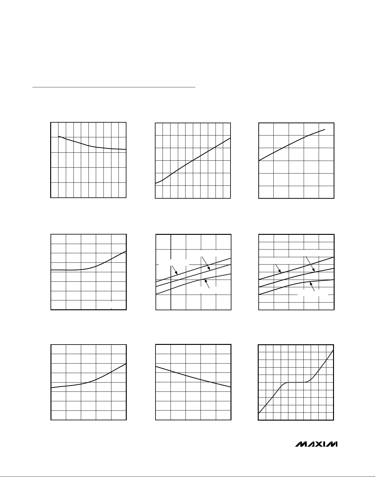
Typical Operating Characteristics
(VCC= +5V, VEE= -5.2V, RL= 50Ω to VT, VT= -2V, V
OD
= 10mV, TA= +25°C, unless otherwise noted.)
WORST-CASE PROPAGATION DELAY
vs. INPUT OVERDRIVE
1400
1200
1000
800
PROPAGATION DELAY (ps)
600
400
0405020 3010 60 70 80 90 100
INPUT OVERDRIVE (mV)
MAX9691/3-01
WORST-CASE PROPAGATION DELAY
vs. TEMPERATURE
1400
1300
1200
1100
1000
900
PROPAGATION DELAY (ps)
800
700
600
-40 -15 10 35 60 85
TEMPERATURE (°C)
VOD = 100mV
MAX9691/3-04
WORST-CASE PROPAGATION DELAY
vs. SOURCE IMPEDANCE
6000
5000
4000
3000
2000
PROPAGATION DELAY (ps)
1000
0
0 20015050 100 250 300 350 400 450 500
SOURCE IMPEDANCE (Ω)
OUTPUT HIGH VOLTAGE
vs. TEMPERATURE
-0.6
-0.7
R
PULLDOWN
-0.8
(V)
OH
V
-0.9
-1.0
-1.1
-40 10-15 35 60 85
R
PULLDOWN
= 200Ω
R
PULLDOWN
TEMPERATURE (°C)
= 100Ω
= 50Ω
1800
MAX9691/3-02
1600
1400
1200
1000
PROPAGATION DELAY (ps)
800
600
0105 152025
-1.60
-1.62
MAX9691/3-05
-1.64
-1.66
-1.68
(V)
-1.70
OL
V
-1.72
-1.74
-1.76
-1.78
-1.80
-40 10-15 35 60 85
WORST-CASE PROPAGATION DELAY
vs. C
LOAD
C
(pF)
LOAD
OUTPUT LOW VOLTAGE
vs. TEMPERATURE
R
= 100Ω
PULLDOWN
R
= 200Ω
PULLDOWN
R
= 50Ω
PULLDOWN
TEMPERATURE (°C)
MAX9691/3-03
MAX9691/3-06
INPUT OFFSET VOLTAGE
vs. TEMPERATURE
2000
1500
1000
500
0
-500
-1000
INPUT OFFSET VOLTAGE (µV)
-1500
-2000
-40 -15 10 35 60 85
TEMPERATURE (°C)
MAX9691/3-08
8.0
7.5
7.0
6.5
6.0
5.5
INPUT BIAS CURRENT (µA)
5.0
4.5
4.0
-40 -15 10 35 60 85
INPUT BIAS CURRENT
vs. TEMPERATURE
TEMPERATURE (°C)
5000
4000
MAX9691/3-09
3000
2000
1000
0
-1000
-2000
INPUT BIAS CURRENT (µA)
-3000
-4000
-5000
-5 -3 -2 -1-4 012 435
INPUT BIAS CURRENT
vs. DIFFERENTIAL INPUT VOLTAGE
DIFFERENTIAL INPUT VOLTAGE (V)
MAX9691/3-10
Page 5

MAX9691/MAX9692/MAX9693
Single/Dual, Ultra-Fast, ECL-Output
Comparators with Latch Enable
_______________________________________________________________________________________
5
Typical Operating Characteristics (continued)
(VCC= +5V, VEE= -5.2V, RL= 50Ω to VT, VT= -2V, V
OD
= 10mV, TA= +25°C, unless otherwise noted.)
PROPAGATION DELAY
MAX9691/3-11
V
IN
200mV/div
1ns/div
Q OUT - Q OUT
200mV/div
VIN = 100mV
V
OD
= 10mV
100MHz OUTPUT RESPONSE
MAX9691/3-12
-1.0V
Q OUT
200mV/div
Q OUT
200mV/div
-1.8V
-1.8V
-1.0V
1ns/div
Pin Description
PIN
MAX9691
11211VCCPositive Supply. Bypass to GND with a 0.1µF capacitor.
2 2 3 — IN+ Positive Input
3 3 4 — IN- Negative Input
4686VEENegative Supply. Bypass to GND with a 0.1µF capacitor.
5 7 11 — Q OUT Output
6 8 12 — Q OUT Complimentary Output
7 9 16 — GND2 Device Ground
8 10 1 — GND1 Device Ground
—4
— 5 6 — LE Latch Enable Input
— — — 1 Q OUTA Channel A Output
——— 2Q OUTA Channel A Complementary Output
— — — 3, 14 GND Device Ground
— — — 4 LEA Channel A Latch Enable Input
——— 5LEA Channel A Latch Enable Complementary Input
— — — 7 INA- Channel A Negative Input
— — — 8 INA+ Channel A Positive Input
— — — 9 INB+ Channel B Positive Input
— — — 10 INB- Channel B Negative Input
———12LEB Channel B Latch Enable Complementary Input
— — — 13 LEB Channel B Latch Enable Input
———15Q OUTB Channel B Complementary Output
— — — 16 Q OUTB Channel B Output
MAX9692
µMAX
MAX9692
PDIP/SO
5, 7, 9, 10,
13, 14, 15
MAX9693
— N.C. No Connection. Not internally connected.
NAME FUNCTION
Page 6

MAX9691/MAX9692/MAX9693
Single/Dual, Ultra-Fast, ECL-Output
Comparators with Latch Enable
6 _______________________________________________________________________________________
__________ Applications Information
Layout
Because of the MAX9691/MAX9692/MAX9693s’ large
gain-bandwidth characteristic, special precautions
must be taken to use them. A PC board with a ground
plane is mandatory. Mount 0.01µF ceramic decoupling
capacitors as close to the power-supply pins as possible, and process the ECL outputs in microstrip fashion,
consistent with the load termination of 50Ω to 200Ω (for
VT = -2V). For low-impedance applications, microstrip
layout and terminations at the input may also be helpful. Pay close attention to the bandwidth of the decoupling and terminating components. Chip components
can be used to minimize lead inductance. Connect
GND1 and GND2 together to a solid copper ground
plane for the MAX9691/MAX9692. GND1 biases the
input gain stages, while GND2 biases the ECL output
stage. If the LE function is not used, connect the LE pin
to GND (MAX9692/MAX9693) and the complementary
LE to ECL logic high level (MAX9693 only). Do not
leave the inputs of an unused comparator floating for
the MAX9693.
Input Slew-Rate Requirements
As with all high-speed comparators, the high gainbandwidth product of these devices creates oscillation
problems when the input goes through the linear
region. For clean switching without oscillation or steps
in the output waveform, the input must meet certain
minimum slew-rate requirements. The tendency of the
part to oscillate is a function of the layout and source
impedance of the circuit employed. Poor layout and
larger source impedance will increase the minimum
slew-rate requirement.
Figure 1 shows a high-speed receiver application with
50Ω input and output termination. With this configuration, in which a ground plane and microstrip PC board
are used, the minimum slew rate for clean output
switching is 1V/µs.
In many applications, adding regenerative feedback
will assist the input signal through the linear region,
which will lower the minimum slew-rate requirement
considerably. For example, with the addition of positive
feedback components, R
f
= 1kΩ and Cf = 10pF, the
minimum slew-rate requirement can be reduced by a
factor of four.
As high-speed receivers, the MAX9691/MAX9692/
MAX9693 are capable of processing signals in excess
of 600MHz. Figure 2 is a 100MHz example with an
input signal level of 14mV
RMS
.
Figure 1. Regenerative Feedback—High-Speed Receiver with
50
Ω
Input and Output Termination
Figure 2. Signal Processed at 100MHz with Input Signal Level
of 14mV
RMS
V
IN
50Ω
50Ω
Q
Q
LE
R
C
f
f
50Ω
-2V
50Ω
INPUT
20mV/div
OUTPUT
500mV/div
2ns/div
0V
-0.9V
-1.7V
Page 7

MAX9691/MAX9692/MAX9693
The timing diagram (Figure 3) illustrates the series of
events that complete the compare function, under
worst-case conditions. The top line of the diagram illustrates two latch-enable pulses. Each pulse is high for
the compare function and low for the latch function. The
first pulse demonstrates the compare function; part of
the input action takes place during the compare mode.
The second pulse demonstrates a compare function
interval during which there is no change in the input.
The leading edge of the input signal (illustrated as a
large-amplitude, small-overdrive pulse) switches the
comparator after time interval t
pd
. Output Q and Q tran-
sistors are similar in timing. The input signal must occur
at time tsbefore the latch falling edge, and must be
maintained for time thafter the edge to be acquired.
After th, the output is no longer affected by the input status until the latch is again strobed. A minimum latch
pulse width of t
pw(LE)
is needed for the strobe opera-
tion, and the output transitions occur after a time t
LE(±)
.
The MAX9691/MAX9692/MAX9693 will not false trip
(i.e., output invert) if one of the inputs is in the valid
common-mode range while the other input is outside
the common-mode range.
Figure 3. Timing Diagram
Single/Dual, Ultra-Fast, ECL-Output
Comparators with Latch Enable
_______________________________________________________________________________________ 7
LATCH
ENABLE
LATCH
DIFFERENTIAL
INPUT
VOLTAGE
V
IN
COMPARE
t
s
t
h
50%
t
pw(LE)
V
OS
Q
Q
V
OD
t
pd
t
LE(+)
50%
50%
Page 8

MAX9691/MAX9692/MAX9693
Single/Dual, Ultra-Fast, ECL-Output
Comparators with Latch Enable
8 _______________________________________________________________________________________
Definition of Terms
V
OS
Input Offset Voltage. The voltage required
between the input terminals to obtain 0V differential at the output.
V
IN
Input Voltage Pulse Amplitude
V
OD
Input Voltage Overdrive
t
pd+
Input to Output High Delay. The propagation
delay measured from the time the input signal
crosses the input offset voltage to the 50%
point of an output low-to-high transition.
t
pd-
Input to Output Low Delay. The propagation
delay measured from the time the input signal
crosses the input offset voltage to the 50%
point of an output high-to-low transition.
t
LE(+)
Latch-Enable to Output High Delay. The prop-
agation delay measured from the 50% point of
the latch-enable signal low-to-high transition
to the 50% point of an output low-to-high transition.
t
LE(-)
Latch-Enable to Output Low Delay. The prop-
agation delay measured from the 50% point of
the latch-enable signal low-to-high transition
to the 50% point of an output high-to-low transition.
t
pw
(LE)
Latch-Enable Pulse Width. The minimum time
the latch-enable signal must be high to acquire
and hold an input signal.
t
s
Setup Time. The minimum time before the
negative transition of the latch-enable pulse
that an input signal must be present to be acquired and held at the outputs.
t
h
Hold Time. The minimum time after the negative transition of the latch-enable signal that
an input signal must remain unchanged to be
acquired and held at the output.
∆
pd
Propagation Delay Skew. The difference in
propagation delay between the Q and Q outputs crossing each other in both directions.
P
DSP
Propagation Delay Dispersion. The change in
propagation delay as a result of the overdrive
of the input signal varying.
t
pdm
Propagation Delay Match (MAX9693 only).
The difference in propagation delay between
two separate channels.
Ordering Information (continued)Chip Information
PROCESS: BiCMOS
Note: Devices are also available in lead(Pb)-free/RoHS-compliant packages. Specify lead-free by adding a “+” after the part
number.
PART
MAX9692EUB -40°C to +85°C 10 µMAX
MAX9692ESE -40°C to +85°C 16 Narrow SO
MAX9692EPE -40°C to +85°C 16 PDIP
MAX9693ESE -40°C to +85°C 16 Narrow SO
MAX9693EEE -40°C to +85°C 16 QSOP
MAX9693EPE -40°C to +85°C 16 PDIP
TEMP
RANGE
PIN-PACKAGE
Page 9

MAX9691/MAX9692/MAX9693
Pin Configurations
TOP VIEW
Single/Dual, Ultra-Fast, ECL-Output
Comparators with Latch Enable
_______________________________________________________________________________________ 9
Package Information
For the latest package outline information and land patterns (footprints), go to www.maxim-ic.com/packages. Note that a "+", "#", or
"-" in the package code indicates RoHS status only. Package drawings may show a different suffix character, but the drawing pertains to the package regardless of RoHS status.
MAX9692
MAX9691
1
V
CC
2
IN+
3
IN-
4
5
LE
10
GND1
9
GND2
8
Q OUT
7
Q OUTN.C.
6
V
EE
µMAX
MAX9692
1
GND1 GND2
2
V
CC
IN+
3
4
IN-
N.C.
5
6
LE
7
N.C.
V
8
EE
16
15
N.C.
14
N.C.
13
N.C.
Q OUT
12
Q OUT
11
10
N.C.
9
N.C.
PDIP/SO
1
V
CC
2
3
IN-
4
EE
87GND1
GND2IN+
Q OUT
6
Q OUTV
5
DIP/SO/µMAX
MAX9693
1
Q OUTA Q OUTB
2
Q OUTA
GND
3
4
LEA
LEA
5
6
V
EE
7
INA-
INA+
8
16
15
Q OUTB
14
GND
13
LEB
12
LEB
V
11
CC
10
INB-
9
INB+
DIP/SO/QSOP
PACKAGE TYPE PACKAGE CODE OUTLINE NO.
8 µMAX U8+1 21-0036 90-0092
8 SO S8+2 21-0041 90-0096
8 PDIP P8+5 21-0043 —
10 µMAX U10+2 21-0061 90-0330
16 QSOP E16+1 21-0055 90-0167
16 SO S16+3 21-0041 90-0097
16 PDIP P16+1 21-0043 —
LAND
PATTERN NO.
Page 10

MAX9691/MAX9692/MAX9693
Single/Dual, Ultra-Fast, ECL-Output
Comparators with Latch Enable
10 ______________________________________________________________________________________
Package Information (continued)
For the latest package outline information and land patterns (footprints), go to www.maxim-ic.com/packages. Note that a "+", "#", or
"-" in the package code indicates RoHS status only. Package drawings may show a different suffix character, but the drawing pertains to the package regardless of RoHS status.
D
D
α
α
Page 11

MAX9691/MAX9692/MAX9693
Package Information (continued)
For the latest package outline information and land patterns (footprints), go to www.maxim-ic.com/packages. Note that a "+", "#", or
"-" in the package code indicates RoHS status only. Package drawings may show a different suffix character, but the drawing pertains to the package regardless of RoHS status.
Single/Dual, Ultra-Fast, ECL-Output
Comparators with Latch Enable
______________________________________________________________________________________ 11
Page 12

MAX9691/MAX9692/MAX9693
Single/Dual, Ultra-Fast, ECL-Output
Comparators with Latch Enable
Maxim cannot assume responsibility for use of any circuitry other than circuitry entirely embodied in a Maxim product. No circuit patent licenses are
implied. Maxim reserves the right to change the circuitry and specifications without notice at any time. The parametric values (min and max limits) shown in
the Electrical Characteristics table are guaranteed. Other parametric values quoted in this data sheet are provided for guidance.
12
____________________Maxim Integrated Products, 120 San Gabriel Drive, Sunnyvale, CA 94086 408-737-7600
© 2012 Maxim Integrated Products Maxim is a registered trademark of Maxim Integrated Products, Inc.
Revision History
REVISION
NUMBER
0 8/00 Initial release —
1 10/02 Updated Ordering Information. 7
2 1/12 Revised Ordering Information, Absolute Maximum Ratings, and Pin Description. 1, 2, 5, 7
REVISION
DATE
DESCRIPTION
PAGES
CHANGED
 Loading...