19-2400; Rev 1; 7/93
Dual, Ultra-Fast ECL-Output Comparator
_______________General Description
The MAX9687 is a dual, ultra-fast ECL comparator
manufactured with a high-frequency bipolar process
(fT= 6GHz) capable of very short propagation delays.
This design maintains the excellent DC matching characteristics normally found only in slower comparators.
The MAX9687 is pin-compatible with the AD9687 and
Am6687, but exceeds their AC characteristics.
The MAX9687 has differential inputs and complementary outputs that are fully compatible with ECL-logic levels. Output current levels are capable of driving 50Ω
terminated transmission lines. The ultra-fast operation
makes signal processing possible at frequencies in
excess of 600MHz.
A latch-enable (LE) function is provided to allow the
comparator to be used in a sample/hold or track/hold
mode. The latch-enable inputs are designed to be driven from the complementary outputs of a standard ECL
gate. When LE is high and –L—E–is low, the comparator
functions normally. When LE is forced low and –L—E–is
high, the comparator outputs are locked in the logical
states determined by the input conditions at the time of
the latch transition. If the latch-enable function is not
used on either of the two comparators, the appropriate
LE input must be connected to ground; the companion
–L—E–
input can be left open.
________________________Applications
High-Speed A/D Converters
High-Speed Line Receivers
Peak Detectors
Threshold Detectors
High-Speed Triggers
____________________________Features
♦ 1.4ns Propagation Delay
♦ 0.5ns Latch Setup Time
♦ 2.0ns Latch-Enable Pulse Width
♦ +5V, -5.2V Power Supplies
♦ Pin-Compatible with AD9687, Am6687, SP9687
♦ Available in Commercial, Extended-Industrial,
and Military Temperature Ranges
♦ Available in Narrow SO Package
______________Ordering Information
PART TEMP. RANGE PIN-PACKAGE*
MAX9687CPE 0°C to +70°C 16 Plastic DIP
MAX9687CSE 0°C to +70°C 16 Narrow SO
MAX9687CJE 0°C to +70°C 16 CERDIP
MAX9687C/D 0°C to +70°C Dice**
MAX9687EPE -40°C to +85°C 16 Plastic DIP
MAX9687ESE -40°C to +85°C 16 Narrow SO
MAX9687MJE -55°C to +125°C 16 CERDIP
* Contact factory for availability of 20-pin PLCC.
** Contact factory for dice specifications.
MAX9687
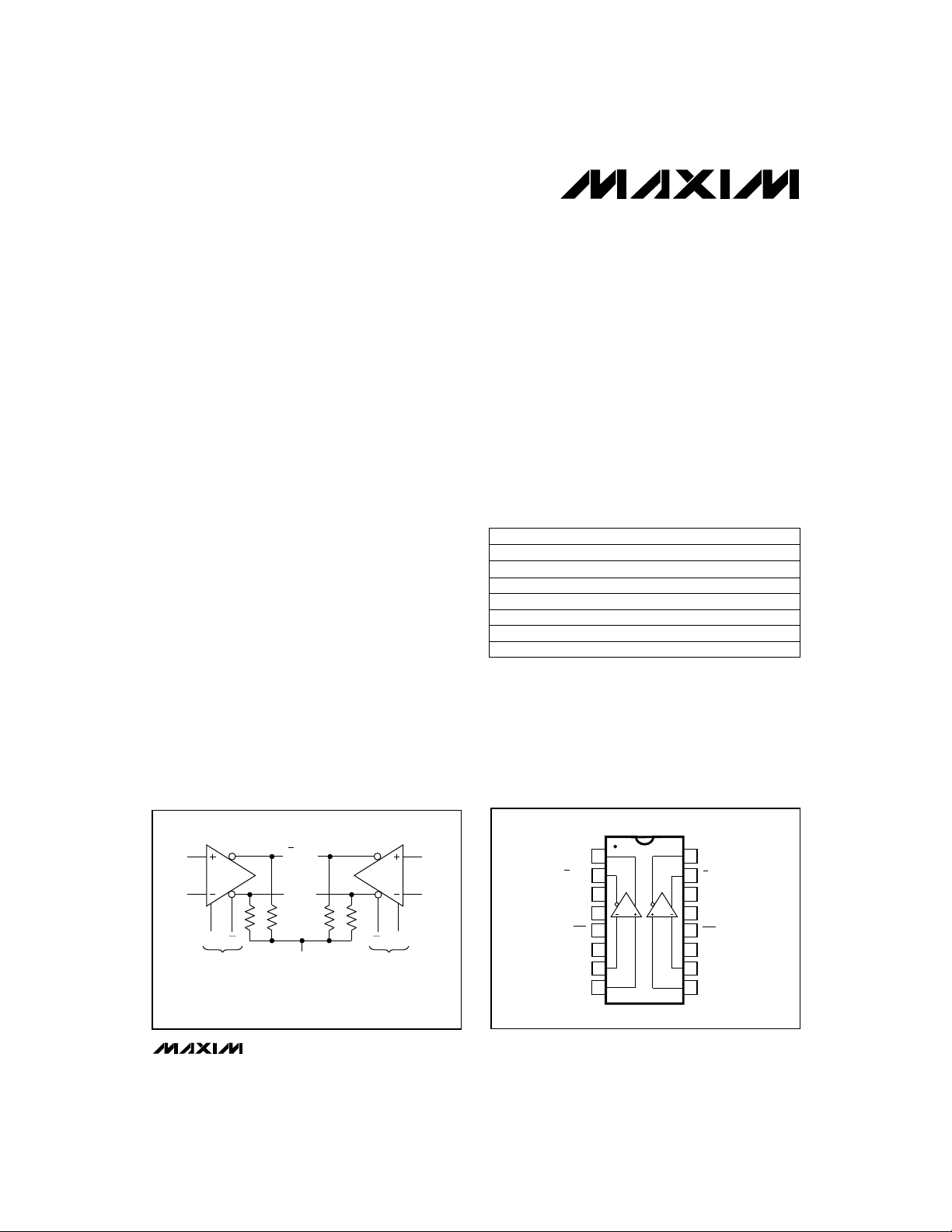
________________Functional Diagram
NONINVERTING
INPUT
INVERTING
INPUT
R
L
LE LE
LATCH ENABLE
THE OUTPUTS ARE OPEN EMITTERS, REQUIRING EXTERNAL PULL-DOWN
RESISTORS. THESE RESISTORS MAY BE IN THE RANGE OF 50Ω – 200Ω
CONNECTED TO -2.0V, OR 240Ω – 2000Ω CONNECTED TO -5.2V.
Q OUT
Q OUT
R
R
L
L
V
T
________________________________________________________________
R
L
LE LE
LATCH ENABLE
NONINVERTING
INPUT
INVERTING
INPUT
___________________Pin Configuration
TOP VIEW
1
Q OUT
2
Q OUT
3
GND
LEA
LEA
INA-
INA+
A
4
5
6
V-
7
8
DIP/SO
Maxim Integrated Products
Call toll free 1-800-998-8800 for free samples or literature.
16
Q OUT
15
Q OUT
14
GND
B
13
LEB
12
LEB
11
V+
10
INB-
9
INB+
1

Dual, Ultra-Fast ECL-Output Comparator
ABSOLUTE MAXIMUM RATINGS
Supply Voltages.....................................................................±6V
Output Short-Circuit Duration (Note 1)..........................Indefinite
Input Voltages........................................................................±5V
Differential Input Voltages.....................................................3.5V
Output Current....................................................................30mA
Continuous Power Dissipation (T
Plastic DIP (derate 10.53mW/°C above +70°C) ...........842mW
= +70°C)
A
Narrow SO (derate 8.70mW/°C above +70°C) .............696mW
CERDIP (derate 10.00mW/°C above +70°C)................800mW
MAX9687
Note 1: Continuous short-circuit protection is allowed on one comparator at a time up to case temperatures of +85°C and ambient
temperatures of +30°C.
Stresses beyond those listed under “Absolute Maximum Ratings” may cause permanent damage to the device. These are stress ratings only, and functional
operation of the device at these or any other conditions beyond those indicated in the operational sections of the specifications is not implied. Exposure to
absolute maximum rating conditions for extended periods may affect device reliability.
ELECTRICAL CHARACTERISTICS
(VS= ±15V, VCM= 0V, TA= +25°C, unless otherwise noted.)
PARAMETER SYMBOL
to T
to T
TA= +25°C
TA= T
MAX
MAX
TA= T
TA= T
TA= +25°C
TA= T
TA= T
Input Offset Voltage
(Note 2)
Temperature Coefficient ∆V
Input Offset Current I
Input Bias Current I
Input Voltage Range V
Common-Mode
Rejection Ratio
Power-Supply Rejection
Ratio
Input Resistance R
Input Capacitance C
Logic Output
High Voltage
V
RS= 100Ω
OS
/
∆T 10 µV/°C
OS
TA= +25°C
OS
TA= T
MIN
TA= +25°C
B
TA= T
MIN
(Note 2)
CM
CMRR 80 dB
(Note 2)
PSRR 60 dB
(Note 2)
IN
IN
MAX9687C,
MAX9687M
V
OH
MAX9687E
TA= +25°C
TA= T
TA= T
TA= +25°C
TA= T
TA= T
Logic Output
Low Voltage
MAX9687C,
MAX9687M
V
OL
MAX9687E
TA= +25°C
Positive Supply Current
Negative Supply Current
I
CC
I
EE
MIN
MIN
to T
to T
MAX
MAX
Operating Temperature Ranges
MAX9687C_ E.....................................................0°C to +70°C
MAX9687E_ E..................................................-40°C to +85°C
MAX9687MJE ................................................-55°C to +125°C
Storage Temperature Range.............................-55°C to +150°C
Lead Temperature (soldering, 10sec).............................+300°C
MIN
to T
MIN TYP MAX
MAX
MAX9687C/E
-5 5
-7 7
MAX9687M
MIN TYP MAX
-5 5
-8 8
15
5
8
10 20
10 20
30
-2.5 +2.5 V
-2.5 +2.5
80
60
MIN
MAX
MIN
MAX
60 kΩ
3 pF
-0.89 -0.70
-0.96 -0.81
-1.14 -0.88
-0.88 -0.70
60
3
-1.16 -0.89-1.05 -0.87
-0.88 -0.69
-0.96 -0.81
-0.96 -0.81
MIN
MAX
MIN
MAX
-1.89 -1.65
-1.83 -1.57
-1.85 -1.65
-1.90 -1.65
-1.83 -1.57
-1.90 -1.65
-1.82 -1.55
-1.85 -1.65
-1.85 -1.65
30 4630 46TA= +25°C
54 6854 68TA= +25°C
5
12
40
5250TA= T
7472TA= T
UNITSCONDITIONS
mV
µA
µA
V
V
mA
mA
2 _______________________________________________________________________________________
 Loading...