

19-2400; Rev 1; 7/93
Dual, Ultra-Fast ECL-Output Comparator
_______________General Description
The MAX9687 is a dual, ultra-fast ECL comparator
manufactured with a high-frequency bipolar process
(fT= 6GHz) capable of very short propagation delays.
This design maintains the excellent DC matching characteristics normally found only in slower comparators.
The MAX9687 is pin-compatible with the AD9687 and
Am6687, but exceeds their AC characteristics.
The MAX9687 has differential inputs and complementary outputs that are fully compatible with ECL-logic levels. Output current levels are capable of driving 50Ω
terminated transmission lines. The ultra-fast operation
makes signal processing possible at frequencies in
excess of 600MHz.
A latch-enable (LE) function is provided to allow the
comparator to be used in a sample/hold or track/hold
mode. The latch-enable inputs are designed to be driven from the complementary outputs of a standard ECL
gate. When LE is high and –L—E–is low, the comparator
functions normally. When LE is forced low and –L—E–is
high, the comparator outputs are locked in the logical
states determined by the input conditions at the time of
the latch transition. If the latch-enable function is not
used on either of the two comparators, the appropriate
LE input must be connected to ground; the companion
–L—E–
input can be left open.
________________________Applications
High-Speed A/D Converters
High-Speed Line Receivers
Peak Detectors
Threshold Detectors
High-Speed Triggers
____________________________Features
♦ 1.4ns Propagation Delay
♦ 0.5ns Latch Setup Time
♦ 2.0ns Latch-Enable Pulse Width
♦ +5V, -5.2V Power Supplies
♦ Pin-Compatible with AD9687, Am6687, SP9687
♦ Available in Commercial, Extended-Industrial,
and Military Temperature Ranges
♦ Available in Narrow SO Package
______________Ordering Information
PART TEMP. RANGE PIN-PACKAGE*
MAX9687CPE 0°C to +70°C 16 Plastic DIP
MAX9687CSE 0°C to +70°C 16 Narrow SO
MAX9687CJE 0°C to +70°C 16 CERDIP
MAX9687C/D 0°C to +70°C Dice**
MAX9687EPE -40°C to +85°C 16 Plastic DIP
MAX9687ESE -40°C to +85°C 16 Narrow SO
MAX9687MJE -55°C to +125°C 16 CERDIP
* Contact factory for availability of 20-pin PLCC.
** Contact factory for dice specifications.
MAX9687
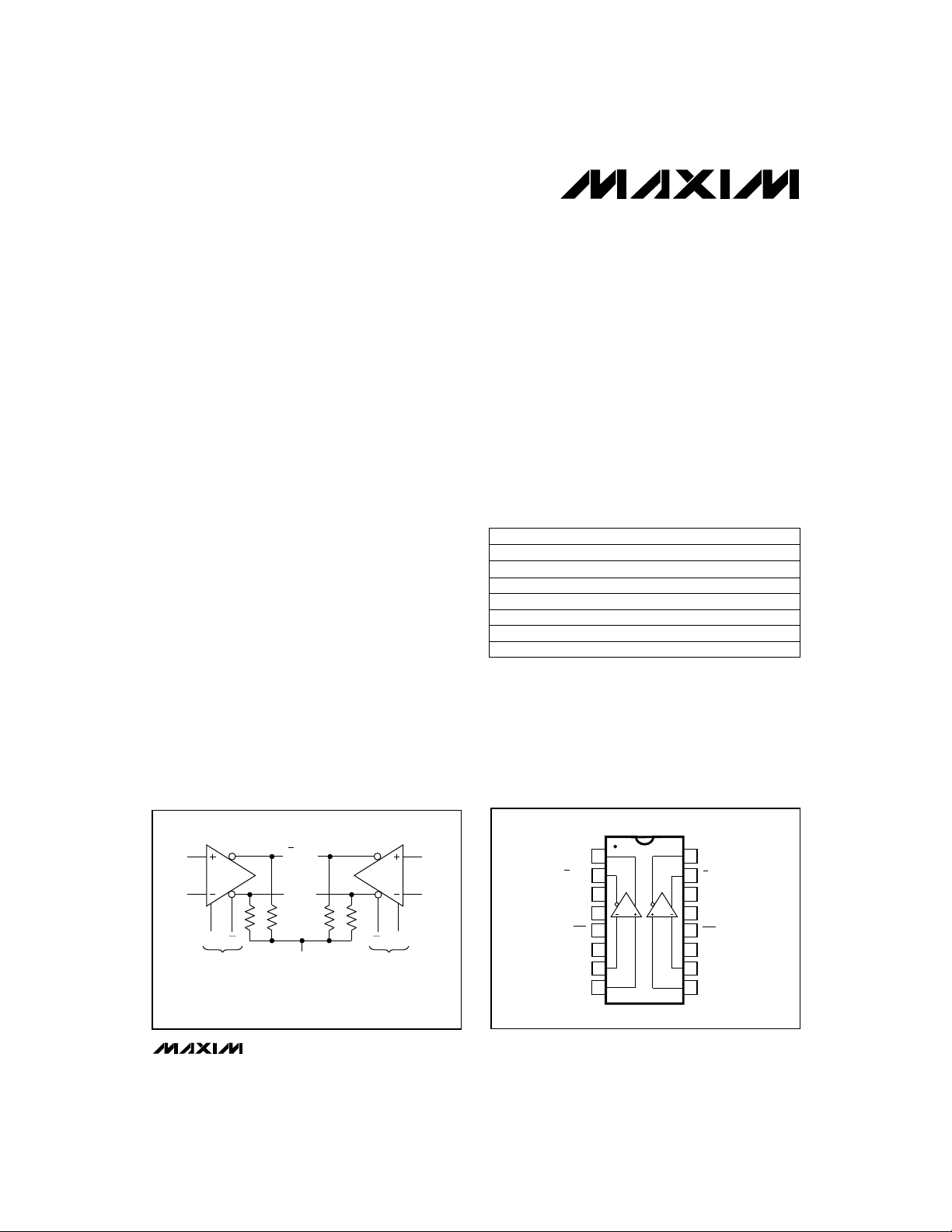
________________Functional Diagram
NONINVERTING
INPUT
INVERTING
INPUT
R
L
LE LE
LATCH ENABLE
THE OUTPUTS ARE OPEN EMITTERS, REQUIRING EXTERNAL PULL-DOWN
RESISTORS. THESE RESISTORS MAY BE IN THE RANGE OF 50Ω – 200Ω
CONNECTED TO -2.0V, OR 240Ω – 2000Ω CONNECTED TO -5.2V.
Q OUT
Q OUT
R
R
L
L
V
T
________________________________________________________________
R
L
LE LE
LATCH ENABLE
NONINVERTING
INPUT
INVERTING
INPUT
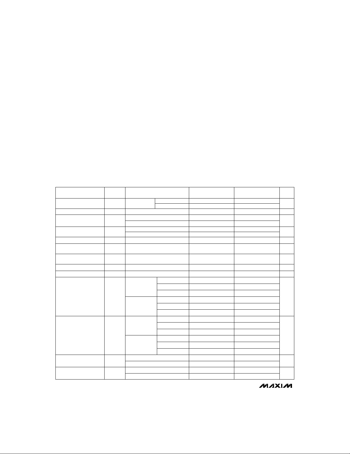
___________________Pin Configuration
TOP VIEW
1
Q OUT
2
Q OUT
3
GND
LEA
LEA
INA-
INA+
A
4
5
6
V-
7
8
DIP/SO
Maxim Integrated Products
Call toll free 1-800-998-8800 for free samples or literature.
16
Q OUT
15
Q OUT
14
GND
B
13
LEB
12
LEB
11
V+
10
INB-
9
INB+
1
Dual, Ultra-Fast ECL-Output Comparator
ABSOLUTE MAXIMUM RATINGS
Supply Voltages.....................................................................±6V
Output Short-Circuit Duration (Note 1)..........................Indefinite
Input Voltages........................................................................±5V
Differential Input Voltages.....................................................3.5V
Output Current....................................................................30mA
Continuous Power Dissipation (T
Plastic DIP (derate 10.53mW/°C above +70°C) ...........842mW
= +70°C)
A
Narrow SO (derate 8.70mW/°C above +70°C) .............696mW
CERDIP (derate 10.00mW/°C above +70°C)................800mW
MAX9687
Note 1: Continuous short-circuit protection is allowed on one comparator at a time up to case temperatures of +85°C and ambient
temperatures of +30°C.
Stresses beyond those listed under “Absolute Maximum Ratings” may cause permanent damage to the device. These are stress ratings only, and functional
operation of the device at these or any other conditions beyond those indicated in the operational sections of the specifications is not implied. Exposure to
absolute maximum rating conditions for extended periods may affect device reliability.
ELECTRICAL CHARACTERISTICS
(VS= ±15V, VCM= 0V, TA= +25°C, unless otherwise noted.)
PARAMETER SYMBOL
to T
to T
TA= +25°C
TA= T
MAX
MAX
TA= T
TA= T
TA= +25°C
TA= T
TA= T
Input Offset Voltage
(Note 2)
Temperature Coefficient ∆V
Input Offset Current I
Input Bias Current I
Input Voltage Range V
Common-Mode
Rejection Ratio
Power-Supply Rejection
Ratio
Input Resistance R
Input Capacitance C
Logic Output
High Voltage
V
RS= 100Ω
OS
/
∆T 10 µV/°C
OS
TA= +25°C
OS
TA= T
MIN
TA= +25°C
B
TA= T
MIN
(Note 2)
CM
CMRR 80 dB
(Note 2)
PSRR 60 dB
(Note 2)
IN
IN
MAX9687C,
MAX9687M
V
OH
MAX9687E
TA= +25°C
TA= T
TA= T
TA= +25°C
TA= T
TA= T
Logic Output
Low Voltage
MAX9687C,
MAX9687M
V
OL
MAX9687E
TA= +25°C
Positive Supply Current
Negative Supply Current
I
CC
I
EE
MIN
MIN
to T
to T
MAX
MAX
Operating Temperature Ranges
MAX9687C_ E.....................................................0°C to +70°C
MAX9687E_ E..................................................-40°C to +85°C
MAX9687MJE ................................................-55°C to +125°C
Storage Temperature Range.............................-55°C to +150°C
Lead Temperature (soldering, 10sec).............................+300°C
MIN
to T
MIN TYP MAX
MAX
MAX9687C/E
-5 5
-7 7
MAX9687M
MIN TYP MAX
-5 5
-8 8
15
5
8
10 20
10 20
30
-2.5 +2.5 V
-2.5 +2.5
80
60
MIN
MAX
MIN
MAX
60 kΩ
3 pF
-0.89 -0.70
-0.96 -0.81
-1.14 -0.88
-0.88 -0.70
60
3
-1.16 -0.89-1.05 -0.87
-0.88 -0.69
-0.96 -0.81
-0.96 -0.81
MIN
MAX
MIN
MAX
-1.89 -1.65
-1.83 -1.57
-1.85 -1.65
-1.90 -1.65
-1.83 -1.57
-1.90 -1.65
-1.82 -1.55
-1.85 -1.65
-1.85 -1.65
30 4630 46TA= +25°C
54 6854 68TA= +25°C
5
12
40
5250TA= T
7472TA= T
UNITSCONDITIONS
mV
µA
µA
V
V
mA
mA
2 _______________________________________________________________________________________

Dual, Ultra-Fast ECL-Output Comparator
SWITCHING CHARACTERISTICS
(VS= ±5V, TA= +25°C, unless otherwise noted.)
PARAMETER SYMBOL
Input to Output High
(Notes 2, 3)
Input to Output Low
(Notes 2, 3)
Latch-Enable to Output High
(Notes 2, 3)
Latch-Enable to Output Low
(Notes 2, 3)
Minimum Setup Time t
Note 2: Not tested, guaranteed by design.
Note 3: VIN= 100mV, VOD= 10mV.
50Ω
V
IN
f
50Ω
t
pd+
t
pd-
t
(E) ns
pd+
t
(E)
pd-
tpw(E)
s
h
LE
50Ω
CfR
50Ω
CONDITIONS
TA= +25°C
TA= 0°C to +70°C 1.6 2.2
TA= -55°C to +125°C
TA= +25°C 1.4 1.9
TA= -55°C to +125°C
TA= +25°C
TA= 0°C to +70°C
TA= -55°C to +125°C
TA= +25°C 1.4 1.8
TA= 0°C to +70°C
TA= -55°C to +125°C
-2V
MAX9687C/E
MIN TYP MAX
1.4 1.9
1.6 2.2TA= 0°C to +70°C
1.3 1.8
1.4 2.0
3.0 2.0
0.5 1.0
0.5 1.0
INPUT
20mV/div 2ns/div
INPUT
OUTPUT
MIN TYP MAX
OUTPUT
500mV/div
MAX9687M
3.0 2.0Latch-Enable Pulse Width (Note 2)
1.4 1.9
1.7 2.6
1.4 1.9
1.9 2.6
1.3 1.8
1.5 2.0
1.3 1.8
1.7 2.6
0.5 1.0
0.5 1.0Minimum Hold Time t
MAX9687
UNITS
ns
ns
ns1.6 1.9
ns
0V
-0.9V
Figure 1. High-speed receiver application with 50Ωinput and output termination. With this configuration, in which a ground plane and
microstrip PC board was used, the minimum slew rate for clean output switching is 1.6V/µs. For sine-wave inputs, this implies a minimum signal size of 360mV
Slew Rate
E
=
RMS
2f2
π
at 500MHz and 90mV at 2MHz.
RMS
__________Applications Information
Because of the MAX9687’s large gain-bandwidth characteristic, special precautions need to be taken if its highspeed capabilities are to be used. A PC board with a
ground plane is mandatory. Mount all decoupling capacitors as close to the power-supply pins as possible, and
process the ECL outputs in microstrip fashion, consistent
with the load termination of 50Ω to 120Ω. For low-imped-
_______________________________________________________________________________________ 3
Layout
-1.7V
Figure 2. As a high-speed receiver, the MAX9687 is capable of
processing signals in excess of 600MHz. Figure 2 is a 100MHz
example with an input signal level of 14mV
RMS.
ance applications, microstrip layout at the input may also
be helpful. Pay close attention to the bandwidth of the
decoupling and terminating components. Chip components can be used to minimize lead inductance.
Input Slew-Rate Requirement
As with all high-speed comparators, the high gainbandwidth product of these devices creates oscillation
problems when the input traverses through the linear
region. For clean switching without oscillation or steps
in the output waveform, the input must meet certain

Dual, Ultra-Fast ECL-Output Comparator
minimum slew-rate requirements. The tendency of the
part to oscillate is a function of the layout and source
impedance of the circuit employed. Both poor layout
and larger source impedance will increase the minimum slew-rate specification.
In many applications, the addition of regenerative feedback will assist the input signal through the linear
region, which will lower the minimum slew-rate requirement considerably. For example, with the addition of
MAX9687
positive feedback components Rf = 1kΩ and
Cf = 10pF, the minimum slew-rate requirement can be
reduced by a factor of four.
____________________Timing Diagram
The timing diagram (Figure 3) illustrates the series of
events that complete the compare function, under
worst-case conditions.
The top line of the diagram illustrates two latch-enable
(LE) pulses; each pulse is high for the compare function and low for the latch function. The first pulse
demonstrates the compare function in which part of the
input action takes place during the compare mode.
The second pulse demonstrates a compare-function
interval during which there is no change in the input.
The leading edge of the input signal (illustrated as a
large-amplitude, small-overdrive pulse) switches the
comparator after time interval tpd. Outputs Q and –Q
are similar in timing. The input signal must occur at time
tsbefore the latch falling edge and, to be acquired,
must be maintained for time thafter the edge. After th,
the output is no longer affected by the input status until
the latch is again strobed. A minimum latch pulse width
of tpw(E) is needed for the strobe operation, and the
output transitions occur after a time tpd(E).
COMPARE
LATCH
ENABLE
DIFFERENTIAL
INPUT
VOLTAGE
LATCH
V
IN
Q
t
s
t
h
V
OD
t
pd
V
Input Offset Voltage—The voltage required
OS
between the input terminals to obtain 0V differential at the output.
Definition of Terms
V
Input Voltage Pulse Amplitude
IN
V
Input Voltage Overdrive
OD
t
Input to Output High Delay—The propagation
pd+
delay measured from the time the input signal
crosses the input offset voltage to the 50% point
of an output low-to-high transition.
t
Input to Output Low Delay—The propagation
pd-
delay measured from the time the input signal
crosses the input offset voltage to the 50% point
of an output high-to-low transition.
t
(E) Latch-Enable to Output High Delay—The propa-
pd+
gation delay measured from the 50% point of the
latch-enable signal low-to-high transition to the
50% point of an output low-to-high transition.
t
(E) Latch-Enable to Output Low Delay—The propa-
pd-
gation delay measured from the 50% point of the
latch-enable signal low-to-high transition to the
50% point of an output high-to-low transition.
tpw(E) Minimum Latch-Enable Pulse Width—The mini-
mum time the latch-enable signal must be high
–
to acquire and hold an input signal.
t
Minimum Setup Time—The minimum time before
s
the negative transition of the latch-enable pulse
that an input signal must be present to be
acquired and held at the outputs.
t
Minimum Hold Time—The minimum time after
h
the negative transition of the latch-enable signal
that an input signal must remain unchanged to
be acquired and held at the outputs.
50%
tpw (E)
V
OS
tpd (E)
50%
Q
Figure 3. Timing Diagram
Maxim cannot assume responsibility for use of any circuitry other than circuitry entirely embodied in a Maxim product. No circuit patent licenses are
implied. Maxim reserves the right to change the circuitry and specifications without notice at any time.
4
___________________Maxim Integrated Products, 120 San Gabriel Drive, Sunnyvale, CA 94086 (408) 737-7600
© 1993 Maxim Integrated Products Printed USA is a registered trademark of Maxim Integrated Products.
50%
 Loading...