

Page 1
19-4904; Rev 1; 12/10
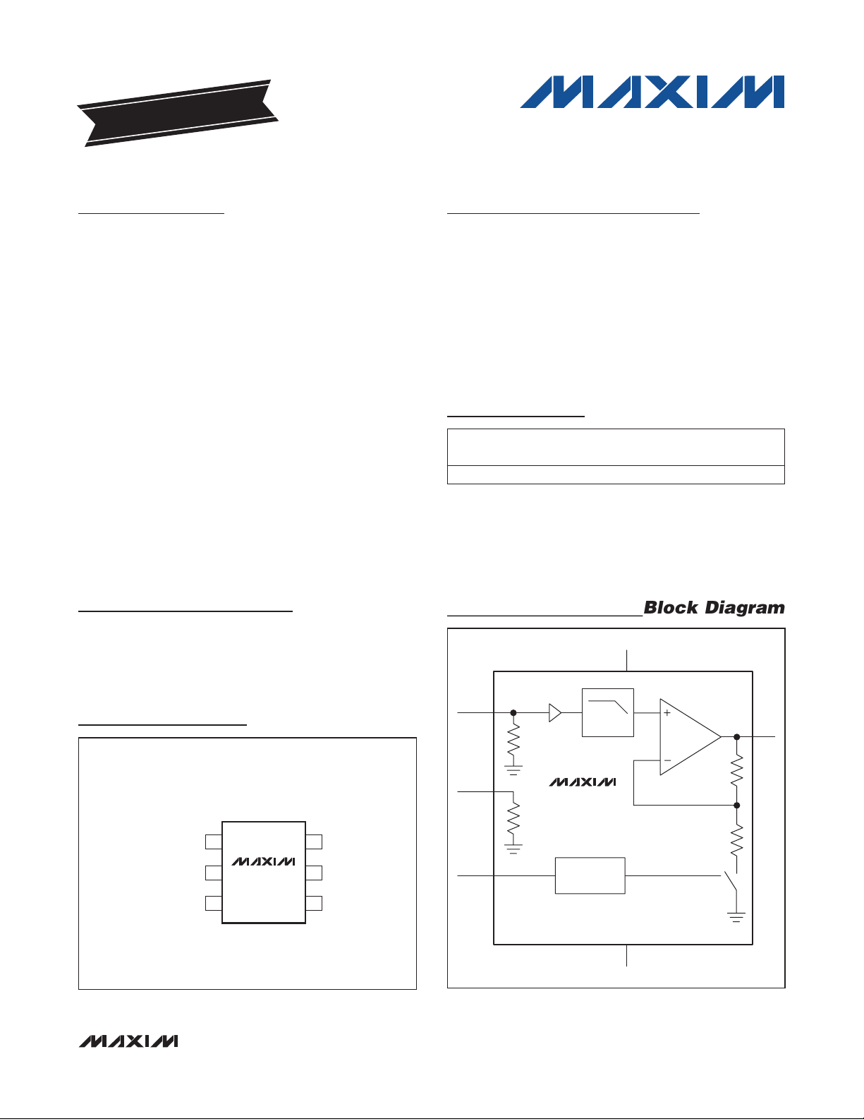
Block Diagram
EVALUATION KIT
AVAILABLE
Internal Gain and Filter in SC70
General Description
The MAX9680 high-speed amplifier and filter is optimized for portable video applications. It is specifically designed to be compatible with the video encoders
embedded in application processors with 0.4V
output. The input common-mode range includes GND,
which allows a video DAC (digital-to-analog converter)
to be DC-coupled to the MAX9680.
The output swings within 2mV of GND and 20mV to VDD
with a standard back-terminated video load (150I). An
internal level shift circuit prevents the output from saturating with 0V input, thus preventing sync-pulse clipping
in common video circuits. Therefore, the MAX9680 is
ideally suited for DC-coupling to the video load.
The MAX9680 has been optimized for space-sensitive
applications by integrating internal gain setting resistors
(G = 5.2V/V) and a 2-pole video-DAC reconstruction filter.
In shutdown mode, the quiescent current is reduced to
less than 0.4FA, dramatically reducing power consumption and prolonging battery life.
The MAX9680 is available in the tiny 2mm x 2.1mm,
6-pin, SC70 package.
P-P
video
3V Video Amplifier with
Features
S 5.2V/V Internal Gain
S 2-Pole Reconstruction Filter
S Input Range Includes Ground
S DC-Coupled Inputs and Outputs
S Rail-to-Rail Output
S 3.7mA Low Quiescent Current
S 0.4µA Shutdown Current
Ordering Information
PART
MAX9680AXT+T
+Denotes a lead(Pb)-free/RoHS-compliant package.
T = Tape and reel.
Typical Application Circuit appears at end of data sheet.
TEMP
RANGE
-40NC to +125NC
PIN-
PACKAGE
6 SC70 ADT
TOP
MARK
MAX9680
Applications
Mobile Phones
Digital Still Cameras
Digital Video Cameras
Pin Configuration
TOP VIEW
+
GND
RSET
IN
1
2
MAX9680
3
SC70
6
5
4
V
DD
ENABLE
OUT
RSET
ENABLE
V
DD
IN
MAX9680
SHUTDOWN
CONTROL
LPF
OUT
G = 5.2V/V
GND
BUFFER
R
IN
R
SET
_______________________________________________________________ Maxim Integrated Products 1
For pricing, delivery, and ordering information, please contact Maxim Direct at 1-888-629-4642,
or visit Maxim’s website at www.maxim-ic.com.
Page 2
3V Video Amplifier with
Internal Gain and Filter in SC70
ABSOLUTE MAXIMUM RATINGS
Supply Voltage (VDD to GND) .................................-0.3V to +4V
ENABLE to GND ......................................................-0.3V to +4V
IN to GND ................................................. -0.3V to (VDD + 0.3V)
OUT to GND (ENABLE is high) ................ -0.3V to (VDD + 0.3V)
OUT to GND (ENABLE is low) .............................-0.3V to +3.2V
ENABLE, IN ..................................................................... Q50mA
OUT ...........................................................................Continuous
Electrostatic Discharge
MAX9680
Human Body Model .......................................................2000V
Charged Device Model ...................................................500V
PACKAGE THERMAL CHARACTERISTICS (Note 1)
SC70
Junction-to-Ambient Thermal Resistance (qJA) .....326.5°C/W
Junction-to-Case Thermal Resistance (qJC) .............115°C/W
Note 1: Package thermal resistances were obtained using the method described in JEDEC specification JESD51-7, using a 4-layer
board. For detailed information on package thermal considerations, refer to www.maxim-ic.com/thermal-tutorial.
Stresses beyond those listed under “Absolute Maximum Ratings” may cause permanent damage to the device. These are stress ratings only, and functional
operation of the device at these or any other conditions beyond those indicated in the operational sections of the specifications is not implied. Exposure to absolute
maximum rating conditions for extended periods may affect device reliability.
ELECTRICAL CHARACTERISTICS
(V
= V
DD
= +25NC.) (Note 2)
OFFSET LEVEL-SHIFT VOLTAGE
Output Level-Shift Voltage V
Power-Supply Rejection Ratio PSRR VIN = V
INPUT VOLTAGE RANGE
Input Voltage Range V
Input Resistance (In+) R
R
Resistance R
SET
R
SET/RIN
VOLTAGE GAIN
DC Voltage Gain (Note 3) A
FREQUENCY RESPONSE
Filter Response
Differential Gain Error
Differential Phase Error
= 2.8V, V
ENABLE
PARAMETER SYMBOL CONDITIONS MIN TYP MAX UNITS
Ratio 4.214 4.3 4.386
= 0V, RL = 150I to GND. TA = -40NC to +125NC, unless otherwise noted. Typical values are at TA
GND
OLS
CM
SET
VIN = V
GND
GND
VDD = 2.7V V
VDD = 2.8V V
VIN = 0.5V 732 872 1012
IN
V
= 0.5V 3150 3750 4350
RSET
VDD = 2.7V, VIN = V
V
VDD = 2.8V, VIN = V
VIN = V
0.387V
Five-step modulated staircase of 127.8mV
step size and 305.3mV peak-to-peak
subcarrier amplitude, f = 4.43MHz
Five-step modulated staircase of 127.8mV
step size and 305.3mV peak-to-peak
subcarrier amplitude, f = 4.43MHz
GND
to
Continuous Power Dissipation (TA = +70NC)
6-Pin SC70 (derate 3.1mW/C above +70NC) .............245mW
Operating Temperature Range ........................ -40NC to +125NC
Junction Temperature .....................................................+150NC
Storage Temperature Range ............................ -65NC to +150NC
Lead Temperature (soldering, 10s) ................................+300NC
Soldering Temperature (reflow) ......................................+260NC
0 120 250 mV
, VDD = 2.7V to 3.6V 200
GND
GND
to 0.445V 5.00 5.17 5.34
GND
to 0.464V 5.00 5.17 5.34
GND
f = 4.5MHz -0.2
f = 9MHz -3.5
f = 27MHz -23
f = 54MHz -45
0.2 %
0.3 degrees
0.445
0.464
FV/V
V
I
I
V/V
dB
2 ______________________________________________________________________________________
Page 3
3V Video Amplifier with
Internal Gain and Filter in SC70
ELECTRICAL CHARACTERISTICS (continued)
(V
= V
DD
= +25NC.) (Note 2)
Group Delay Variation
Signal-to-Noise Ratio SNR 100% white signal 65 dB
OUTPUT
Positive Voltage Output Swing
from Rail
Negative Voltage Output Swing
from Rail
Positive Voltage Output Swing
from Rail
Negative Voltage Output Swing
from Rail
Output Leakage Disabled, V
Output Short-Circuit Current I
POWER SUPPLY
Supply Voltage V
Supply Current I
ENABLE/SHUTDOWN FUNCTION
Disabled (Logic-Low Threshold) 0 0.45 V
Enabled (Logic-High Threshold) 1.3 V
Enable Time 350 ns
Disable Time 200 ns
Shutdown Current Disabled 0.4 4
Note 2: All devices are 100% production tested at TA = +25NC. Specifications over temperature limits are guaranteed by design.
Note 3: Voltage gain (AV) is a two-point measurement in which the output voltage swing is divided by the input voltage swing.
ENABLE
= 2.8V, V
= 0V, RL = 150I to GND. TA = -40NC to +125NC, unless otherwise noted. Typical values are at TA
GND
PARAMETER SYMBOL CONDITIONS MIN TYP MAX UNITS
100kHz P f P 5.5MHz, VIN = V
GND
to 0.387V
15 ns
VIN = 0.7V 20 250 mV
VIN = -0.05V 1.8 5 mV
35 mV
1 mV
FA
DD
OUT
DD
DD
VIN = 0.7V, RL = 75I to GND
VIN = -0.05V, RL = 75I to GND
= 2V 2
OUT
Short to GND 90 mA
2.7 3.6 V
No load 3.7 9 mA
FA
V
MAX9680
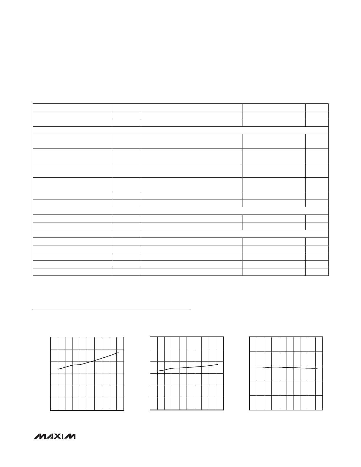
Typical Operating Characteristics
(V
= V
DD
INPUT RESISTANCE vs. TEMPERATURE
890
885
880
875
870
INPUT RESISTANCE (I)
865
860
-60 140
ENABLE
= 2.8V, V
V
IN
TEMPERATURE (°C)
= 0V, RL = 150I to GND. TA = +25NC, unless otherwise noted.)
GND
= 0.4V
MAX9680 toc01
120100806040200-20-40
SET RESISTANCE vs. TEMPERATURE
3900
3850
3800
3750
3700
SET RESISTANCE (I)
3650
3600
-60 140
TEMPERATURE (°C)
R
vs. TEMPERATURE
4.5
MAX9680 toc02
4.4
4.3
(I/I)
IN
/R
SET
4.2
R
4.1
120100806040200-20-40
4.0
SET/RIN
TEMPERATURE (°C)
_______________________________________________________________________________________ 3
120100806040200-20-40-60 140
MAX9680 toc03
Page 4

3V Video Amplifier with
Internal Gain and Filter in SC70
Typical Operating Characteristics (continued)
(V
DD
= V
ENABLE
= 2.8V, V
= 0V, RL = 150I to GND. TA = +25NC, unless otherwise noted.)
GND
5.5
5.4
MAX9680
5.3
GAIN (V/V)
5.2
5.1
5.0
TEMPERATURE (°C)
OUTPUT VOLTAGE LEVEL SHIFT
vs. TEMPERATURE
V
0.200
0.175
0.150
0.125
0.100
0.075
0.050
OUTPUT VOLTAGE LEVEL SHIFT (V)
0.025
0
TEMPERATURE (
GAIN vs. TEMPERATURE
120100806040200-20-40-60 140
5
MAX9680 toc04
4
3
2
OUTPUT VOLTAGE (mV)
1
0
OUTPUT VOLTAGE vs. TEMPERATURE
= -50mV
V
IN
120100806040200-20-40-60 140
TEMPERATURE (°C)
MAX9680 toc05
OUTPUT VOLTAGE vs. TEMPERATURE
= 700mV
V
2.90
2.85
2.80
2.75
2.70
OUTPUT VOLTAGE (V)
2.65
2.60
-60 140
IN
TEMPERATURE (°C)
MAX9680 toc06
120100806040200-20-40
OUTPUT LEAKAGE CURRENT
= V
IN
GND
120100806040200-20-40-60 140
°C)
9
8
MAX9680 toc07
7
6
5
QUIESCENT CURRENT (mA)
4
3
-60 140
= 2.8V
V
ENABLE
TEMPERATURE (°C)
100
MAX9680 toc08
10
1
0.1
OUTPUT LEAKAGE CURRENT (nA)
100806040200-20-40
120
0.01
QUIESCENT CURRENT vs. TEMPERATURE
vs. TEMPERATURE
ENABLE = GND, V
TEMPERATURE (°C)
OUT
= 2V
MAX9680 toc09
120100806040200-20-40-60 140
OUTPUT LEAKAGE CURRENT
vs. TEMPERATURE, ENABLE = 0
100
90
80
70
60
50
40
30
20
OUTPUT LEAKAGE CURRENT (nA)
10
0
SHORT TO V
TEMPERATURE (°C)
MAX9680 toc10
CC
SHORT TO GND
120100806040200-20-40-60 140
SHUTDOWN QUIESCENT CURRENT
HYSTERESIS vs. TEMPERATURE
10
1
0.1
QUIESCENT CURRENT (mA)
TA = +125°C
0.01
0.6 1.0
ENABLE VOLTAGE (V)
TA = +25°C
TA = -40°C
0.90.80.7
MAX9680 toc11
0
GAIN vs. FREQUENCY
-5
-10
-15
-20
GAIN (dB)
-25
-30
-35
-40
100 100,000
FREQUENCY (kHz)
4 ______________________________________________________________________________________
MAX9680 toc12
10,0001000
Page 5

3V Video Amplifier with
Internal Gain and Filter in SC70
Typical Operating Characteristics (continued)
(V
DD
= V
ENABLE
= 2.8V, V
= 0V, RL = 150I to GND. TA = +25NC, unless otherwise noted.)
GND
MAX9680
V
CC
(2V/div)
OUTPUT
(1V/div)
OUTPUT VOLTAGE vs. OUTPUT CURRENT
3.0
2.5
2.0
1.5
TA = 0°C AND +25°C
1.0
OUTPUT VOLTAGE (V)
0.5
0
0 120
TA = +125°C
TA = +85°C
TA = -25°C
TA = -40°C
OUTPUT CURRENT (mA)
TURN-ON TIME
TIME (200ns/div)
MAX9680 toc15
10080604020
MAX9680 toc13
GND
GND
OUTPUT VOLTAGE
vs. OUTPUT SINKING CURRENT
3.0
2.5
2.0
1.5
1.0
OUTPUT VOLTAGE (V)
0.5
0
TA = 0°C
TA = -25°C
TA = -40°C
0 3.0
OUTPUT CURRENT (mA)
V
(2V/div)
OUTPUT
(1V/div)
TA = +125°C
TA = +85°C
TA = +25°C
TURN-OFF TIME
CC
TIME (40ns/div)
MAX9680 toc14
GND
GND
GROUP DELAY vs. FREQUENCY
100
90
MAX9680 toc16
80
70
60
50
DELAY (ns)
40
30
20
10
2.52.01.51.00.5
0
100 100,000
FREQUENCY (kHz)
10,0001000
MAX9680 toc17
POWER-SUPPLY REJECTION RATIO
MAX9680
0
-10
-20
-30
-40
-50
-60
RESPONSE (dB)
-70
-80
-90
-100
0.1 100
VDD = 2.8V ± 100mV
V
ENABLE
RL = 150Ω TO GND
VIN = GND
FREQUENCY (MHz)
= 2.8V
101
_______________________________________________________________________________________ 5
P-P
0.03
0.02
MAX9680 toc17a
0.01
0
-0.01
DIFFERENTIAL GAIN (%)
-0.02
-0.03
DIFFERENTIAL GAIN AND PHASE
f = 4.43MHz
0 1 2 3 4 5
0.6
0.4
MAX9680 toc18
0.2
0
-0.2
DIFFERENTIAL PHASE (deg)
-0.4
-0.6
0 1 2 3 4 5
DIFFERENTIAL GAIN AND PHASE
f = 4.43MHz
MAX9680 toc19
Page 6

3V Video Amplifier with
Internal Gain and Filter in SC70
Pin Description
PIN NAME DESCRIPTION
1 IN Input
2 GND Ground
3 RSET
MAX9680
4 OUT Output
5 ENABLE Enable. Drive high to enable the device. Pull low to disable the device.
6 V
DD
Resistor Set. The reference voltage of the current digital-to-analog converter (DAC) is applied
across the internal R
Positive Power Supply. Bypass to GND with a 0.1FF capacitor.
resistor to generate the reference current of the DAC.
SET
Detailed Description
The MAX9680 filters and amplifies the video DAC output
in applications such as mobile phones. The MAX9680
consists of two resistors, an input buffer, lowpass filter,
and output amplifier capable of driving a standard 150I
video load to ground. The output amplifier provides a
fixed gain of 5.17V/V.
R
Resistor
SET
The video current DAC imposes a reference voltage,
V
, across R
REF
the reference current for the video current DAC.
The video input should be directly connected to the output of the video current DAC. RIN, the equivalent input
resistance, is 872I to ground. The output current of the
video DAC flows through RIN to create the video signal
in the voltage domain.
The filter bandwidth (-3dB) is typically 9MHz, making the
device suitable for standard-definition video signals from
all sources (e.g., broadcast and DVD). Broadcast video
signals are channel limited: NTSC signals have 4.2MHz
bandwidth, and PAL signals have 5MHz bandwidth.
Video signals from a DVD player, however, are not channel limited; so the bandwidth of DVD video signals can
approach the Nyquist limit of 6.75MHz. Recommendation:
ITU-R BT.601-5 specifies 13.5MHz as the sampling rate
. The resulting current (V
SET
REF/RSET
) is
Input
Video Filter
for standard-definition video. Therefore, the maximum
bandwidth of the signal is 6.75MHz. To ease the filtering
requirements, most modern video systems oversample
by two times, clocking the video current DAC at 27MHz.
Output
The MAX9680 features 5.17V/V gain. Operating from a
2.7V to 3.6V supply, the output amplifier is able to drive
a 2.3V signal into a 150I video load to ground. The output is typically offset 120mV above ground to guarantee
linear operation of the amplifier. The MAX9680 output
only sources current; all loads should be connected to
ground.
Short-Circuit Protection
The MAX9680 Typical Application Circuit includes a 75I
back-termination resistor that limits short-circuit currents
for an external short applied at the video output. The
MAX9680 features internal output short-circuit protection
to prevent device damage in prototyping and applications where the amplifier output can be directly shorted.
Short-circuit protection activates if the output is short
circuited and the output current exceeds 90mA. During
short-circuit protection, the output of the MAX9680 is
shut off for 18Fs and then turns on for 0.6Fs. If the short
is still present, the MAX9680 output shuts off again.
Extended short circuits result in a pulsed output. The
device resumes normal operation after the short is
removed.
6 ______________________________________________________________________________________
Page 7

3V Video Amplifier with
Internal Gain and Filter in SC70
Application Information
Input Considerations
The MAX9680 input is DC-coupled. When the supply voltage is between 2.7V and 3.6V, the input voltage range
extends from ground to 0.445V. When the supply voltage is between 2.8V and 3.6V, the input voltage range
extends from ground to 0.464V. A typical current-output
DAC that operates from a single supply usually creates
a composite video signal with a sync tip very close to
ground. Hence, the DAC output can be directly connected to the MAX9680 input. Keep the board trace as
short as possible to minimize parasitic stray capacitance
and prevent unintentional high-frequency attenuation.
The MAX9680 output must be DC-coupled. No
AC-coupled capacitors are allowed. The MAX9680 connects directly to the video cable through a 75I series
back-termination resistor. The other end of the cable
should be properly terminated with a 75I resistor as
well. Because of this configuration, the peak-to-peak
amplitude as well as the DC level of the signal is divided
by two. The MAX9680 output signal is level-shifted up so
the sync tip is approximately 120mV.
Power-Supply Bypassing and Ground
The MAX9680 operates from a single-supply voltage
down to 2.7V, allowing for low-power operation. Bypass
VDD to GND with a 0.1FF capacitor. Place all external
components as close as possible to the device.
Typical Application Circuit
Output Considerations
MAX9680
VIDEO ENCODER
DAC
GENERAL-PURPOSE OUTPUT
RSET
ENABLE
V
= 2.8V
DD
IN
MAX9680
SHUTDOWN
CONTROL
LPF
OUT
75I
G = 5.2V/V
GND
BUFFER
R
IN
R
SET
Chip Information
PROCESS: BiCMOS
_______________________________________________________________________________________ 7
Page 8

3V Video Amplifier with
Internal Gain and Filter in SC70
Package Information
For the latest package outline information and land patterns, go to www.maxim-ic.com/packages. Note that a “+”, “#”, or “-” in the
package code indicates RoHS status only. Package drawings may show a different suffix character, but the drawing pertains to the
package regardless of RoHS status.
PACKAGE TYPE PACKAGE CODE OUTLINE NO. LAND PATTERN NO.
6 SC70 X6SN+1
21-0077 90-0189
MAX9680
8 ______________________________________________________________________________________
Page 9

3V Video Amplifier with
Internal Gain and Filter in SC70
Revision History
MAX9680
REVISION
NUMBER
0 9/09 Initial release —
1 12/10 Added PSRR TOC 5
REVISION
DATE
DESCRIPTION
PAGES
CHANGED
Maxim cannot assume responsibility for use of any circuitry other than circuitry entirely embodied in a Maxim product. No circuit patent licenses are implied.
Maxim reserves the right to change the circuitry and specifications without notice at any time.
Maxim Integrated Products, 120 San Gabriel Drive, Sunnyvale, CA 94086 408-737-7600 9
©
2010 Maxim Integrated Products Maxim is a registered trademark of Maxim Integrated Products, Inc.
 Loading...