

General Description
The MAX9652/MAX9653/MAX9654 are 3.3V, triplechannel, high-definition (HD) video-filter amplifiers.
Specially designed for YPbPr component video signals,
these devices are ideal for a wide range of set-top box
and portable applications. The inputs to the MAX9652/
MAX9653/MAX9654 are AC-coupled. YIN has a synctip clamp while PBIN and PRIN have keyed clamps.
The output buffer has gain of 2V/V and drives a standard back-terminated 75Ω video load.
The passband of the MAX9654 is logic selectable
between standard definition (SD) and high definition. The
MAX9652/MAX9653 have a fixed passband for HD video.
The MAX9654 SD lowpass filter has ±1dB passband out
to 8.5MHz and 57dB attenuation at 27MHz. The
MAX9652/MAX9653/MAX9654 HD lowpass filter have
±1dB passband out to 42MHz and 50dB attenuation at
109MHz.
The devices consume only 9.5mA per channel and
operate from a 3.3V supply. The MAX9653/MAX9654
feature a low-power, 12µA shutdown mode. The
MAX9652/MAX9653/MAX9654 are specified over the
-40°C to +125°C automotive temperature range.
Applications
Features
♦ 9.5mA/Channel Supply Current
♦ Selectable Lowpass Filter for High-Definition or
Standard-Definition Video Signals (MAX9654)
♦ 8.5MHz Standard-Definition Passband with 57dB
Attenuation at 27MHz
♦ 42MHz High-Definition Passband with 50dB
Attenuation at 109MHz
♦ 2V/V Gain
♦ 3.135V to 3.465V Single-Supply Operation
♦ 12µA Shutdown Mode (MAX9653/MAX9654)
MAX9652/MAX9653/MAX9654
3.3V, HD/SD Triple-Channel Filter Amplifiers
with Shutdown
________________________________________________________________
Maxim Integrated Products
1
19-4236; Rev 0; 8/08
For pricing, delivery, and ordering information, please contact Maxim Direct at 1-888-629-4642,
or visit Maxim’s website at www.maxim-ic.com.
EVALUATION KIT
AVAILABLE
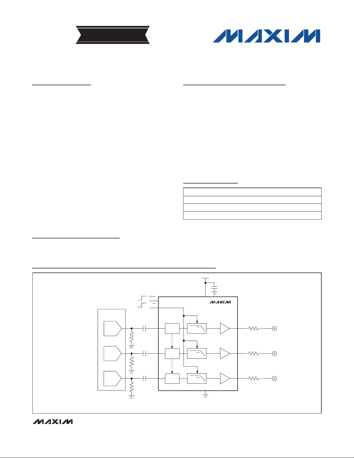
Typical Application Circuit
Ordering Information
Note: All devices are specified over the -40°C to +125°C operating temperature range.
+
Denotes a lead-free/RoHS-compliant package.
T = Tape and reel.
Set-Top Boxes
DVD Players
HDTV
PVR
DVC
PART PIN-PACKAGE FILTER SHUTDOWN
MAX9652ASA+T 8 SO HD No
MAX9653AUB+T 10 µMAX HD Yes
MAX9654AUB+T 10 µMAX SD/HD Yes
+3.3V
0.1μF
V
SD/HD
SD/HD
SD/HD
DD
MAX9652
MAX9653
MAX9654
75Ω
3
3
3
2V/V
2V/V
2V/V
GND
YOUT
PBOUT
PROUT
75Ω
75Ω
2
SHDN
1
SD/HD
MPEG DECODER
0.1μF
0.1μF
0.1μF
PBIN
PRIN
YIN
CLAMP
KEYED
CLAMP
KEYED
CLAMP
CURRENT
DAC
CURRENT
DAC
CURRENT
DAC
1 MAX9654 ONLY.
2 MAX9653 AND MAX9654 ONLY.
3 FOR THE MAX9654, THE PASSBAND IS SELECTABLE BETWEEN SD AND HD. FOR THE MAX9652/MAX9653, THE PASSBAND IS HD.
MAX9652/MAX9653/MAX9654
3.3V, HD/SD Triple-Channel Filter Amplifiers
with Shutdown
2 _______________________________________________________________________________________
ABSOLUTE MAXIMUM RATINGS
ELECTRICAL CHARACTERISTICS
(VDD= 3.3V, V
SHDN
= VDD, V
GND
= 0, no load, TA= T
MIN
to T
MAX
, unless otherwise noted. Typical values are at TA= +25°C.) (Note 1)
Stresses beyond those listed under “Absolute Maximum Ratings” may cause permanent damage to the device. These are stress ratings only, and functional
operation of the device at these or any other conditions beyond those indicated in the operational sections of the specifications is not implied. Exposure to
absolute maximum rating conditions for extended periods may affect device reliability.
VDDto GND..............................................................-0.3V to +4V
YIN, PRIN, PBIN to GND ............................-0.3V to (V
DD
+ 0.3V)
SHDN, SD/HD to GND..............................................-0.3V to +4V
Maximum Current into Any Input Pin ................................±20mA
Output Short-Circuit Current Duration
to V
DD
or GND .......................................................Continuous
Continuous Power Dissipation (T
A
= +70°C)
8-Pin SO (derate 5.9mW/°C above +70°C)..................471mW
10-Pin µMAX (derate 5.6mW/°C above +70°C) .............444mW
Operating Temperature Range .........................-40°C to +125°C
Junction Temperature......................................................+150°C
Storage Temperature Range .............................-65°C to +150°C
Lead Temperature (soldering, 10s) .................................+300°C
PARAMETER SYMBOL CONDITIONS MIN TYP MAX UNITS
DC CHARACTERISTICS
Supply Voltage Range V
Quiescent Supply Current I
Shutdown Supply Current SHDN = GND for MAX9653/MAX9654 12 20 µA
Input Voltage SHDN = GND for MAX9653/MAX9654
Input Resistance (YIN, PBIN,
PRIN)
INPUT
Input Voltage Swing V
YIN Sync Tip Clamp Level V
YIN Input Clamping Current I
YIN Sync Crush
PBIN, PRIN Input Bias Level V
PBIN, PRIN Input Resistance Normal operation, V
OUTPUT
Voltage Gain (Note 2) A
Gain Matching Guaranteed by output voltage swing -2 0 +2 %
Output Level
SWING
DD
DD
CLP
CLP
BIAS
V
Guaranteed by PSRR 3.135 3.3 3.465 V
No load 28.9 45 mA
SHDN = GND for MAX9653/MAX9654 105 210 310 kΩ
Guaranteed by
output voltage swing
V
= V
YIN
CLP
YIN sync-tip clamp
% reduction in sync
pulse from 0.3V;
R
SOURCE
Guaranteed by output voltage swing 1.95 2 2.04 V/V
Sync-tip clamp, YIN = unconnected,
measured at YOUT
PBIN = PRIN = unconnected, measured at
PBOUT, PROUT
= 75Ω
0.3 x
V
Y input 1.3
PB input, PR input 1
0.28 0.34 0.4 V
+ 0.5V 0.62 2.2 µA
Standard definition 0.3
High definition 0.7
0.84 0.915 1 V
= V
SHDN
DD
0.21 0.31 0.41 V
VDD/3
DD
1.1 1.32 1.5 V
0.36 x
V
DD
20 kΩ
V
V
P-P
%

MAX9652/MAX9653/MAX9654
3.3V, HD/SD Triple-Channel Filter Amplifiers
with Shutdown
_______________________________________________________________________________________ 3
ELECTRICAL CHARACTERISTICS (continued)
(VDD= 3.3V, V
SHDN
= VDD, V
GND
= 0, no load, TA= T
MIN
to T
MAX
, unless otherwise noted. Typical values are at TA= +25°C.) (Note 1)
PARAMETER SYMBOL CONDITIONS MIN TYP MAX UNITS
Output Voltage Swing (Note 2)
Output Resistance
Output Leakage
Power-Supply Rejection Ratio 3.135V ≤ VDD ≤ 3.465V 40 57 dB
LOGIC INPUTS
Logic-Low Threshold V
Logic-High Threshold V
Logic-Input Current IIL/I
HIGH DEFINITION
High-Definition Reconstruction
Filter
K2T
Nonlinearity 5-step staircase 0.71 %
Interchannel Time Error
Group Delay Distortion 100kHz ≤ f ≤ 30MHz, VIN = 1V
3.135V ≤ V
3.465V, measured at
output:
= V
V
YIN
+1.3V),
V
PBIN
(V
BIAS
(V
BIAS
V
= 1.3V
YIN
V
PRIN
1.0V
P-P
Normal operation; V
MAX9653/MAX9654
Shutdown; V
MAX9654; T
TA = +25°C
IL
TA = +25°C
IH
VIN = GND to VDD; TA = +25°C 0.01 10 µA
IH
≤
DD
YOUT, RL = 150Ω to
/2
V
VDD
2.535 2.6 2.652
to (V
CLP
CLP
YOUT, RL = 150Ω to
GND
= V
= V
PRIN
- 0.35V) to
+ 0.65V),
P-P
PRIN
SHDN
= +25°C
A
=
PBOUT, PROUT, R
= 150Ω to V
,
=
PBOUT, PROUT, R
= 150Ω to GND
= V
SHDN
DD
= GND for MAX9653/
for
VDD
L
/2
1.95 2.0 2.04
L
0.5 Ω
0.1 10 µA
0.3 x
V
DD
±1dB passband flatness 42 MHz
= 1V
V
IN
P-P
,
reference frequency
is 1MHz
Taken with Tektronix VM5000HD using a
standard matrix signal
f = 30MHz 0.4
f = 50MHz -3
f = 109MHz -50
0.62 %
Difference in time between the 50% point of
the output signals; V
= 0.5V
IN
, Y to Pb
P-P
1ns
and Y to Pr
P-P
7ns
0.7 x
V
DD
V
P-P
V
V
dB
MAX9652/MAX9653/MAX9654
3.3V, HD/SD Triple-Channel Filter Amplifiers
with Shutdown
4 _______________________________________________________________________________________
ELECTRICAL CHARACTERISTICS (continued)
(VDD= 3.3V, V
SHDN
= VDD, V
GND
= 0, no load, TA= T
MIN
to T
MAX
, unless otherwise noted. Typical values are at TA= +25°C.) (Note 1)
Note 1: All devices are 100% production tested at TA= +25°C. Specifications over temperature limits are guaranteed by design.
Note 2: Voltage gain (A
V
) is a two-point measurement in which the output voltage swing is divided by the input voltage swing.
PARAMETER SYMBOL CONDITIONS MIN TYP MAX UNITS
Interchannel Group Delay
Distortion Error
Peak Signal to RMS Noise 100kHz ≤ f ≤ 30MHz 62 dB
Power-Supply Rejection Ratio f = 1MHz, 200mV
Output Impedance f = 30MHz 16 Ω
Crosstalk from Any Active Video
Output to Any Quiet Video Output
STANDARD DEFINITION (MAX9654 Only)
Standard-Definition
Reconstruction Filter
2T Pulse-to-Bar K Rating
2T Pulse Response 2T = 200ns 0.2 K%
2T Bar Response
Nonlinearity 5-step staircase 0.36 %
Interchannel Time Error
Group Delay Distortion 100kHz ≤ f ≤ 5.5MHz +8.7 ns
Interchannel Group Delay
Distortion Error
Peak Signal to RMS Noise 100kHz ≤ f ≤ 5MHz 72 dB
Power-Supply Rejection Ratio f = 1MHz, 200mV
Output Impedance f = 5MHz 3 Ω
Crosstalk from Any Active Video
Output to Any Quiet Video Output
V
= 1V
IN
PBOUT and YOUT to
PROUT
f = 30MHz, video input = 1V
±1dB passband flatness 8.5 MHz
V
= 1V
IN
reference frequency
is 100kHz
2T = 200ns, bar time is 18µs; the beginning
2.5% and the ending 2.5% of the bar time is
ignored
2T = 200ns, bar time is 18µs; the beginning
2.5% and the ending 2.5% of the bar time is
ignored
Difference in time between the 50% point of
the output signals; VIN = 0.5V
and Y to Pr
V
= 1V
IN
PBOUT and YOUT to
PROUT
f = 4.43MHz, video input = 1V
P-P;
P-P
P-P;
,
YOUT to
YOUT to
f = 1MHz 1
f = 10MHz 1
f = 30MHz 1
Y channel 40
P-P
Pb, Pr channels 30
P-P
f = 5.5MHz -0.15
f = 9.6MHz -3
f = 27MHz -57
Y to Pb
P-P;
f = 1MHz 1
f = 3.58MHz 1
f = 4.43MHz 1
Y channel 30
P-P
Pb, Pr channels 25
P-P
-65 dB
0.15 K%
0.15 K%
1ns
-75 dB
ns
dB
dB
ns
dB
MAX9652/MAX9653/MAX9654
3.3V, HD/SD Triple-Channel Filter Amplifiers
with Shutdown
_______________________________________________________________________________________ 5
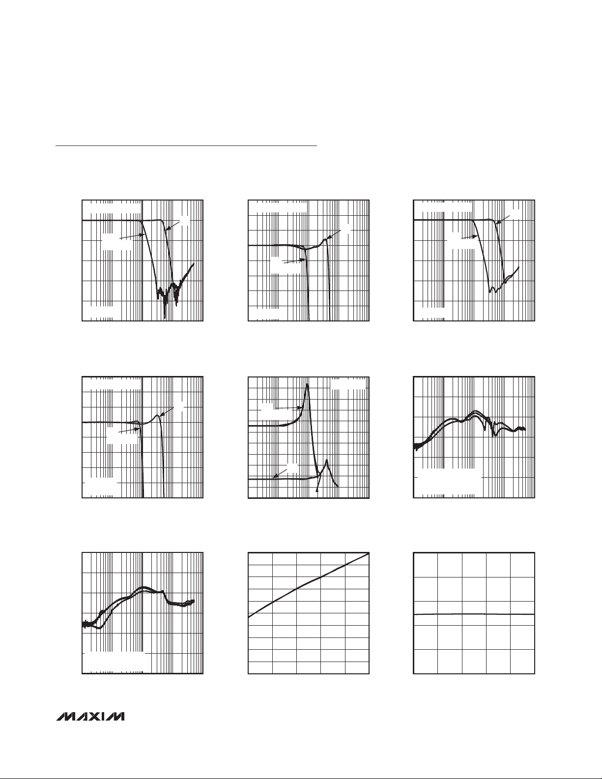
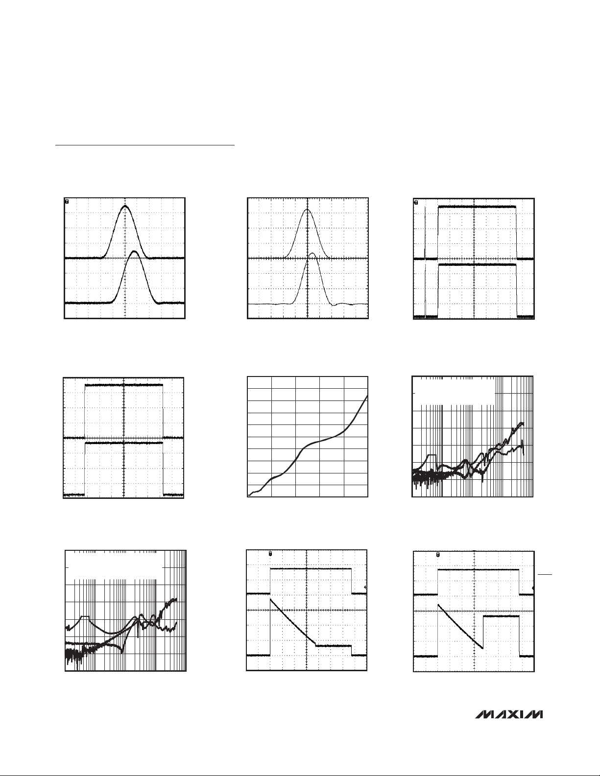
Typical Operating Characteristics
(VDD= +3.3V, video outputs have RL= 150Ω connected to GND unless otherwise stated, V
SHDN
= VDDfor MAX9653/MAX9654.)
SMALL-SIGNAL GAIN
vs. FREQUENCY
20
NORMALIZED TO 0dB
0
-20
-40
GAIN (dB)
-60
-80
-100
SD
(MAX9654)
VIN = 0.1V
P-P
0.1 1000
FREQUENCY (MHz)
LARGE-SIGNAL GAIN FLATNESS
vs. FREQUENCY
3
NORMALIZED TO 0dB
2
1
0
-1
GAIN (dB)
-2
-3
-4
-5
0.1 1000
VIN = 1V
RL = 150Ω
SD
(MAX9654)
P-P
FREQUENCY (MHz)
HD
MAX9652 toc01
GAIN (dB)
100101
HD
100101
MAX9652 toc04
DELAY (ns)
SMALL-SIGNAL GAIN FLATNESS
vs. FREQUENCY
3
NORMALIZED TO 0dB
2
1
0
-1
-2
-3
-4
-5
SD
(MAX9654)
VIN = 0.1V
P-P
0.1 1000
FREQUENCY (MHz)
HD
100101
GROUP DELAY
vs. FREQUENCY
110
100
90
SD
80
(MAX9654)
70
60
50
40
30
20
10
0
0.1 1000
HD
FREQUENCY (MHz)
VIN = 0.1V
100101
MAX9652 toc02
P-P
MAX9652 toc05
LARGE-SIGNAL GAIN
vs. FREQUENCY
20
NORMALIZED TO 0dB
0
-20
-40
GAIN (dB)
-60
-80
VIN = 1V
-100
0.1 1000
SD
(MAX9654)
P-P
FREQUENCY (MHz)
POWER-SUPPLY REJECTION RATIO
vs. FREQUENCY
20
0
-20
-40
GAIN (dB)
-60
STANDARD DEFINITION
-80
-100
= 3.3V + 200mV
V
DD
MAX9654
0.1 1000
P-P
FREQUENCY (MHz)
HD
MAX9652 toc03
100101
MAX9652 toc06
100101
POWER-SUPPLY REJECTION RATIO
vs. FREQUENCY
20
0
-20
-40
GAIN (dB)
-60
-80
HIGH DEFINITION
= 3.3V + 200mV
V
DD
-100
0.1 1000
P-P
FREQUENCY (MHz)
SUPPLY CURRENT
30.5
vs. TEMPERATURE
30.0
MAX9652 toc07
29.5
29.0
28.5
28.0
27.5
27.0
SUPPLY CURRENT (mA)
26.5
26.0
100101
25.5
-40 125
TEMPERATURE (°C)
925926-7
MAX9652 toc08
VOLTAGE GAIN vs. TEMPERATURE
2.5
2.3
2.1
GAIN (V/V)
1.9
1.7
1.5
-40 125
TEMPERATURE (°C)
MAX9652 toc09
925926-7
MAX9652/MAX9653/MAX9654
3.3V, HD/SD Triple-Channel Filter Amplifiers
with Shutdown
6 _______________________________________________________________________________________
Typical Operating Characteristics (continued)
(VDD= +3.3V, video outputs have RL= 150Ω connected to GND unless otherwise stated, V
SHDN
= VDDfor MAX9653/MAX9654.)
100ns/div
2T PULSE RESPONSE (SD)
Y INPUT
200mV/div
Y OUTPUT
400mV/div
MAX9652 toc10
O
O
20ns/div
2T PULSE RESPONSE (HD)
Y INPUT
200mV/div
Y INPUT
400mV/div
MAX9652 toc11
O
O
4
μs/div
2T BAR RESPONSE (SD)
Y INPUT
200mV/div
Y OUTPUT
400mV/div
MAX9652 toc12
O
O
OUTPUT IMPEDANCE
2T BAR RESPONSE (HD)
μs/div
2
MAX9652 toc13
Y INPUT
200mV/div
O
Y INPUT
400mV/div
O
80
72
64
56
48
40
32
24
OUTPUT IMPEDANCE (Ω)
16
8
0
0 100
vs. FREQUENCY
FREQUENCY (MHz)
CROSSTALK
20
vs. FREQUENCY
STANDARD DEFINITION NONHOSTILE
= 1V + 1V
V
IN-ACTIVE
0
V
= 0.9V
IN-INACTIVE
-20
-40
GAIN (dB)
-60
-80
-100
-120
0.1 1000
P-P
FREQUENCY (MHz)
MAX9652 toc16
100101
ENABLE TIME Y CHANNEL
40ms/div
80604020
MAX9652 toc17
MAX9652 toc14
SHDN
2V/div
O
Y INPUT
500mV/div
O
CROSSTALK
vs. FREQUENCY
20
HIGH DEFINITION NONHOSTILE
= 1V + 1V
V
0
IN-ACTIVE
V
IN-INACTIVE
-20
-40
GAIN (dB)
-60
-80
-100
-120
0.1 1000
P-P
= 0.9V
FREQUENCY (MHz)
ENABLE TIME Pb CHANNEL
40ms/div
100101
MAX9652 toc18
MAX9652 toc15
SHDN
2V/div
O
PB OUTPUT
500mV/div
O

MAX9652/MAX9653/MAX9654
3.3V, HD/SD Triple-Channel Filter Amplifiers
with Shutdown
_______________________________________________________________________________________ 7
Typical Operating Characteristics (continued)
(VDD= +3.3V, video outputs have RL= 150Ω connected to GND unless otherwise stated, V
SHDN
= VDDfor MAX9653/MAX9654.)
ENABLE TIME Pr CHANNEL
40ms/div
DISABLE TIME Pb CHANNEL
MAX9652 toc19
MAX9652 toc21
SHDN
2V/div
O
PR OUTPUT
500mV/div
O
SHDN
2V/div
O
DISABLE TIME Y CHANNEL
20ns/div
DISABLE TIME Pr CHANNEL
MAX9652 toc20
SHDN
2V/div
O
Y OUTPUT
200mV/div
O
MAX9652 toc22
SHDN
2V/div
O
PR OUTPUT
1V/div
O
20ns/div
PB OUTPUT
1V/div
O
20ns/div

MAX9652/MAX9653/MAX9654
Detailed Description
The MAX9652/MAX9653/MAX9654 are HD video-filter
amplifiers that operate from a 3.3V supply. They can be
used to lowpass filter the signal after a video digital-toanalog converter (DAC) or before a video analog-todigital converter (ADC). The inputs to the parts must be
AC-coupled; the outputs can be AC- or DC-coupled.
The average power consumption of the parts is significantly less than the average power consumption of the
5V generation of HD video filter amplifiers. The quiescent power consumption of the MAX9654 is 95mW, and
the average power consumption, which is defined when
the parts drive a 150Ω load to ground with color bars, is
200mW.
The MAX9652 is the simplest member of the family, with
neither selectable SD/HD filters nor shutdown capability. This device is best suited for line-powered equipment such as set-top boxes, DVD players, and A/V
receivers.
The MAX9653 has shutdown capability and is a natural
fit in portable equipment and line-powered equipment
in which standby power consumption is a concern. The
MAX9653 is also an option in SCART set-top boxes with
analog high-definition video outputs. In those designs,
the same triple DAC typically generates both the standard-definition RGB signals that are routed through the
SCART device (refer to the MAX9598 data sheet) and
the high-definition YPbPr signals that are routed
through the MAX9653. Only one signal set is output at
any given time, and so the device connected to the
unused outputs must be shut down.
The MAX9654 has both selectable SD/HD filters and
shutdown capability. The applications of the MAX9654
are similar to those of the MAX9653, but the MAX9654
provides the additional capability to switch between
standard-definition and high-definition formats. The
MAX9654 has a passband (±1dB) of 42MHz for highdefinition signals and a passband of 8.5MHz for standard-definition signals.
Inputs
Video signals must be AC-coupled into the MAX9652/
MAX9653/MAX9654 using 0.1µF capacitors. An input
sync tip clamp sets the DC level for the luma signal at
YIN. Keyed clamps on PBIN and PRIN set the DC bias
of the color difference signals at PBIN and PRIN. When
the input sync tip clamp detects a sync pulse on the
luma signal, it generates a signal that activates the
keyed clamps on PBIN and PRIN.
In shutdown mode, the inputs to the MAX9653 and the
MAX9654 do not distort the video signal in case the
outputs of the video DAC are also connected to another
video circuit such as a dual SCART device. See the
SCART Set-Top Box with Analog HD Outputs
section.
The inputs in shutdown mode are biased at V
DD
/3,
which is sufficiently above ground so that the ESD
diodes never forward bias as the video signal changes.
The input resistance in shutdown is 220kΩ which presents negligible loading on the video current DAC.
HD Video Filter
The MAX9652/MAX9653/MAX9654 have a six-pole,
Butterworth filter with a typical passband (±1dB) of
3.3V, HD/SD Triple-Channel Filter Amplifiers
with Shutdown
8 _______________________________________________________________________________________
Pin Description
PIN
MAX9652 MAX9653 MAX9654
1 1 1 YIN Y Input
23 3V
3 4 4 PBIN Pb Input
4 5 5 PRIN Pr Input
5 6 6 PROUT Pr Output
6 7 7 PBOUT Pb Output
7 8, 9 8 GND Ground
8 10 10 YOUT Y Output
—2 2SHDN
— — 9 SD/HD
NAME FUNCTION
DD
Power Supply. Bypass VDD to GND with a 0.1µF capacitor.
Active-Low Shutdown. Connect SHDN to V
operation and to GND for low power consumption.
Standard-Definition/Active-Low High-Definition Passband
Select (MAX9654)
for normal
DD

42MHz, which is well beyond the 30MHz specification
for high-definition video signals. The typical attenuation
is 30dB at 74.25MHz, which is the sample clock rate for
the first generation of high-definition video DACs. The
typical attenuation is 50dB at 109MHz, which is also a
popular sample clock rate.
SD Video Filter
The MAX9654 has a six-pole Butterworth filter with a
typical passband (±1dB) of 8.5MHz, which makes the
device suitable for standard-definition video signals
from all sources (e.g., broadcast and DVD). Broadcast
video signals are channel limited: NTSC signals have
4.2MHz bandwidth and PAL signals have 5MHz bandwidth. Video signals from a DVD player, however, are
not channel limited, so the bandwidth of DVD video signals can approach the Nyquist limit of 6.75MHz.
Recommendation ITU-R BT.601-5 specifies 13.5MHz as
the sampling rate for standard-definition video.
Therefore, the maximum bandwidth of the signal is
6.75MHz. To ease the filtering requirements, most modern video systems oversample by two times, clocking
the video current DAC at 27MHz. The typical attenuation is 57dB at 27MHz.
Video Amplifier
The output amplifiers have a fixed gain of 2V/V, and
their rail-to-rail output stages are capable of driving
back-terminated 75Ω loads. The output load can be
either DC-coupled or AC-coupled, in which case, use
an AC-coupling capacitor of at least 220µF.
The luma signal at YOUT swings between 0.3V and
2.3V approximately. The color difference signals are
centered around 1.32V.
Short-Circuit Protection
The back-termination resistor in a typical application
limits the short-circuit current if an external short is
applied to the system. Additionally, the output amplifiers have built-in short-circuit protection to prevent
accidental damage when the outputs are directly shorted to either supply or ground for short times.
Digital Control
The MAX9654 passband is selectable between SD and
HD. Pulling SD/HD low results in an HD passband, and
pulling SD/HD high results in a SD passband. The
MAX9652/MAX9653 have a fixed HD passband.
The MAX9653/MAX9654 feature a shutdown mode. Pull
SHDN high for normal operation. Pull SHDN low to put the
devices in shutdown, reducing quiescent current to 12µA
typically and placing the outputs in high impedance.
Applications Information
Power Consumption
The quiescent power consumption and average power
consumption of the MAX9652/MAX9653/MAX9654 are
low because of the 3.3V operation. Quiescent power
consumption is defined when the parts operate without a
load. In this case, the MAX9652/MAX9653/MAX9654
consume approximately 95mW. Average power consumption, which is defined when the MAX9652/
MAX9653/MAX9654 drive a 150Ω load to ground with
color bars, is about 200mW. Table 1 shows the power
consumption with different HD video signals. The supply
voltage is 3.3V. The outputs drive 150Ω loads to ground.
MAX9652/MAX9653/MAX9654
3.3V, HD/SD Triple-Channel Filter Amplifiers
with Shutdown
_______________________________________________________________________________________ 9
Figure 1. (A) MAX9653/MAX9654 Input Circuit in Shutdown
Mode; (B) MAX9653/MAX9654 Equivalent Input Circuit in
Shutdown Mode
Table 1. Power Consumption of the
MAX9652/MAX9653/MAX9654 with
Different HD Video Signals
V
DD
667kΩ
IN_
333kΩ
222kΩ
IN_
V
DD
MAX9653
MAX9654
MAX9653
MAX9654
/3
VIDEO SIGNAL POWER CONSUMPTION (mW)
All black screen 181
All white screen 209
Color bars 200

MAX9652/MAX9653/MAX9654
SCART Set-Top Box
with Analog HD Outputs
In set-top boxes with SCART connectors and cinch
connectors for high-definition YPbPr outputs, a triple
video DAC usually outputs either standard-definition
RGB signals that are routed to the SCART device or
high-definition YPbPr signals that are routed through a
high-definition filter amplifier like the MAX9653 (Figure
2). The set-top box devices have a limited number of
video DACs, and hence, one bank of triple video DACs
switches video format depending upon whether standard-definition RGB or high-definition YPbPr signals are
required.
When RGB signals are desired, the high-definition filter
amplifier should be turned off so that the RGB signals
do not appear on the YPbPr connectors. Similarly, when
YPbPr signals are desired, the RGB outputs of the
SCART device should be muted or shut down. In either
case, the inactive device cannot distort the video signals generated by the DACs.
Power-Supply Bypassing and Ground
The MAX9652/MAX9653/MAX9654 operate from a single-supply voltage of 3.3V, allowing for low-power operation. Bypass VDDto GND with a 0.1µF capacitor.
Place all external components as close as possible to
the device.
Using a Digital Supply
The MAX9652/MAX9653/MAX9654 are designed to
operate from noisy digital supplies. The high PSRR
(50dB at 100kHz) allows the devices to reject the noise
from digital power supplies. If the digital power supply
is very noisy and stripes appear on the television
screen, increase the supply bypass capacitance. An
additional, smaller capacitor in parallel with the main
bypass capacitor can reduce digital supply noise
because the smaller capacitor has lower equivalent
series resistance (ESR) and equivalent series inductance (ESL).
3.3V, HD/SD Triple-Channel Filter Amplifiers
with Shutdown
10 ______________________________________________________________________________________

MAX9652/MAX9653/MAX9654
3.3V, HD/SD Triple-Channel Filter Amplifiers
with Shutdown
______________________________________________________________________________________ 11
Figure 2. Triple DAC is connected to both a SCART device and a high-definition, video-filter amplifier. (A) SCART device is transmitting standard-definition RGB signals while the HD filter amplifier is in shutdown mode; (B) SCART device is not transmitting RGB signals, but the HD filter amplifier device is transmitting high-definition YPbPr signals.
A)
SET-TOP BOX
CHIP
DAC
DAC
DAC
B)
SET-TOP BOX
CHIP
DAC
ENC_R/C_IN
ENC_G_IN
ENC_B_IN
YIN
PBIN
PRIN
SHDN
ENC_R/C_IN
ENC_G_IN
ENC_B_IN
MAX9598
MAX9653
MAX9654
OFF
MAX9598
OFF
TV_R/C_OUT
TV_G_OUT
TV_B_OUT
YOUT
PBOUT
PROUT
TV_R/C_OUT
TV_G_OUT
TV_B_OUT
75Ω
75Ω
75Ω
75Ω
75Ω
75Ω
75Ω
75Ω
75Ω
SCART
CONNECTOR
YPbPr OUTPUTS
SCART
CONNECTOR
DAC
DAC
V
DD
YIN
PBIN
PRIN
SHDN
MAX9653
MAX9654
YOUT
PBOUT
PROUT
75Ω
75Ω
75Ω
YPbPr OUTPUTS

MAX9652/MAX9653/MAX9654
3.3V, HD/SD Triple-Channel Filter Amplifiers
with Shutdown
12 ______________________________________________________________________________________
Block Diagram
+3.3V
V
DD
MAX9652
300mV
MAX9653
MAX9654
UNKNOWN
BIAS
SHDN
SD/HD
2
1
YIN
PBIN
PRIN
1 MAX9654 ONLY.
2 MAX9653 AND MAX9654 ONLY.
3 FOR THE MAX9654, THE PASSBAND IS SELECTABLE BETWEEN SD AND HD. FOR THE MAX9652/MAX9653, THE PASSBAND IS HD.
CLAMP
KEYED
CLAMP
KEYED
CLAMP
SD/HD
SD/HD
SD/HD
3
3
3
GND
2V/V
2V/V
2V/V
YOUT
PBOUT
PROUT

MAX9652/MAX9653/MAX9654
Pin Configurations
Chip Information
PROCESS: BiCMOS
3.3V, HD/SD Triple-Channel Filter Amplifiers
with Shutdown
______________________________________________________________________________________ 13
TOP VIEW
YIN
DD
PBIN
+++
1
2
MAX9652
3
4
SO
87YOUT
GNDV
PBOUT
6
PROUTPRIN
5
YIN
SHDN
V
YIN
SHDN
V
1
2
MAX9654
3
DD
4
5
μMAX
1
2
MAX9653
3
DD
4
5
10
YOUT
9
GND
8
GND
7
PBOUTPBIN
PROUTPRIN
6
μMAX
10
YOUT
9
SD/HD
8
GND
7
PBOUTPBIN
PROUTPRIN
6

MAX9652/MAX9653/MAX9654
3.3V, HD/SD Triple-Channel Filter Amplifiers
with Shutdown
14 ______________________________________________________________________________________
Package Information
(The package drawing(s) in this data sheet may not reflect the most current specifications. For the latest package outline information
go to www.maxim-ic.com/packages
.)

MAX9652/MAX9653/MAX9654
3.3V, HD/SD Triple-Channel Filter Amplifiers
with Shutdown
Maxim cannot assume responsibility for use of any circuitry other than circuitry entirely embodied in a Maxim product. No circuit patent licenses are
implied. Maxim reserves the right to change the circuitry and specifications without notice at any time.
Maxim Integrated Products, 120 San Gabriel Drive, Sunnyvale, CA 94086 408-737-7600 ____________________
15
© 2008 Maxim Integrated Products is a registered trademark of Maxim Integrated Products, Inc.
Package Information (continued)
(The package drawing(s) in this data sheet may not reflect the most current specifications. For the latest package outline information
go to www.maxim-ic.com/packages
.)
α
10LUMAX.EPS
α
 Loading...