

Page 1
General Description
The MAX9650/MAX9651 are single- and dual-channel
VCOM amplifiers with rail-to-rail inputs and outputs. The
MAX9650/MAX9651 can drive up to 1300mA of peak
current per channel and operate up to 20V.
The MAX9650/MAX9651 are designed to source and
sink a high current quickly to hold the VCOM voltage
stable in large TFT-LCD panels.
The MAX9650/MAX9651 feature 40V/µs slew rate and
35MHz bandwidth to quickly settle outputs for 120Hz
frame rate and full HD television.
The MAX9650/MAX9651 feature output short-circuit
protection and thermal shutdown. These devices are
available in exposed pad packages for excellent heat
dissipation.
Applications
TFT-LCD Panels
Instrument Control Voltage Sources
Features
♦ 1300mA Peak Output Current
♦ Rail-to-Rail Inputs and Outputs
♦ Operates Up to 20V
♦ 40V/µs Slew Rate
♦ 35MHz Bandwidth
♦ 5mA Quiescent Current per Channel
♦ Excellent Heat Dissipation (Exposed Pad)
MAX9650/MAX9651
High-Current VCOM Drive Op Amps
for TFT LCDs
________________________________________________________________
Maxim Integrated Products
1
19-4187; Rev 4; 7/10
For pricing, delivery, and ordering information, please contact Maxim Direct at 1-888-629-4642,
or visit Maxim’s website at www.maxim-ic.com.
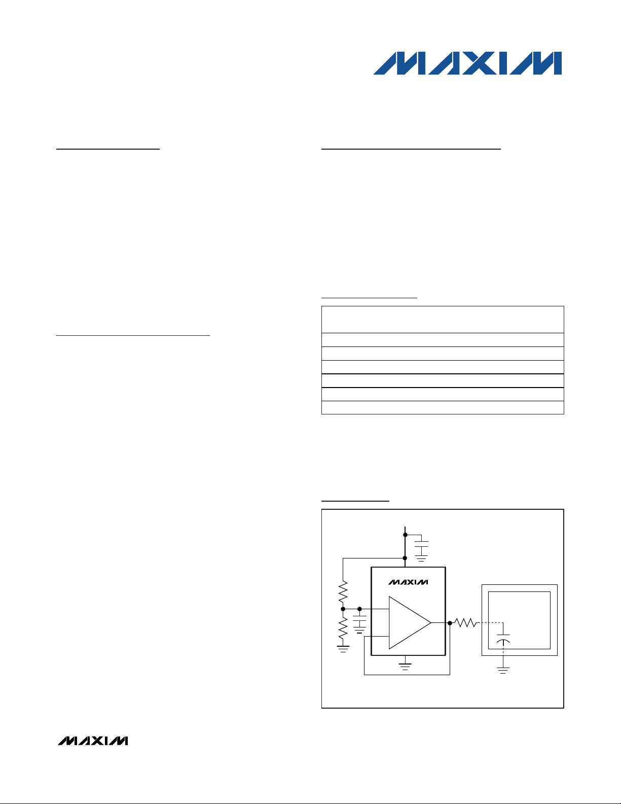
IN_+
IN_-
GND
OUT_
V
DD
TFT LCD
TFT-LCD
CAPACITANCE
16V
V
REF
*RS MAY BE NEEDED FOR SOME APPLICATIONS.
*R
S
MAX9650
Typical Operating Circuit
Ordering Information
PART
AMPS PER
PIN-
TOP MARK
MAX9650AZK+ 1 5 SOT23 ADSI
MAX9650AZK/V+
1 5 SOT23 ADSK
MAX9650AUA+ 1
AABI
MAX9650ATA+ 1
BKX
MAX9651AUA+ 2
AABH
MAX9651ATA+ 2
BKY
Note: All devices are specified over the -40°C to +125°C operating range.
+
Denotes a lead(Pb)-free/RoHS-compliant package.
/V denotes an automotive qualified part.
*
EP = Exposed pad.
PACKAGE
PACKAGE
8 µMAX-EP*
8 TDFN-EP*
8 µMAX-EP*
8 TDFN-EP*
Page 2
MAX9650/MAX9651
High-Current VCOM Drive Op Amps
for TFT LCDs
2 _______________________________________________________________________________________
ABSOLUTE MAXIMUM RATINGS
ELECTRICAL CHARACTERISTICS
(VDD= 19V, V
GND
= 0V, VCM= V
OUT
= VDD/2, TA= T
MIN
to T
MAX
, unless otherwise noted. Typical values are at TA= +25°C.) (Note 1)
Stresses beyond those listed under “Absolute Maximum Ratings” may cause permanent damage to the device. These are stress ratings only, and functional
operation of the device at these or any other conditions beyond those indicated in the operational sections of the specifications is not implied. Exposure to
absolute maximum rating conditions for extended periods may affect device reliability.
Supply Voltage (VDDto GND) ................................-0.3V to +22V
Any Other Pin to GND ................................-0.3V to (V
DD
+ 0.3V)
IN_+/IN_- (current)............................................................±20mA
OUT_ (current) ......................................................................1.3A
Continuous Power Dissipation (T
A
= +70°C)
5-Pin SOT23 (derate 3.7mW/°C above +70°C)........297.4mW
8-Pin µMAX-EP (derate 12.9mW/°C
above +70°C).......................................................1030.9mW
8-Pin TDFN-EP (derate 23.8mW/°C
above +70°C).......................................................1951.2mW
Operating Temperature Range .........................-40°C to +125°C
Junction Temperature......................................................+150°C
Storage Temperature Range .............................-65°C to +150°C
Lead Temperature (soldering, 10s) .................................+300°C
Soldering Temperature (reflow) .......................................+260°C
Supply Voltage Range V
Quiescent Current I
High Output Voltage V
Low Output Voltage V
Input Offset Voltage V
Load Regulation LR
Input Bias Current I
Voltage Gain A
Power-Supply Rejection Ratio PSRR VDD = 6V to 20V, VCM = V
Common-Mode Input Voltage
Range
Common-Mode Rejection Ratio CMRR 0.5V ≤ VCM ≤ VDD - 0.5V 60 80 dB
Continuous Output Current I
Transient Peak Output Current I
Bandwidth BW -3dB 35 MHz
Slew Rate SR 4V step, CL = 50pF, RL = 10kΩ, AV = +1V/V 40 V/µs
Settling Time t
PARAMETER SYMBOL CONDITIONS MIN TYP MAX UNITS
DD
DD
OH
OL
OS
FB
V
CMVR Inferred from CMRR test 0.5
O
PK
S
Guaranteed by PSRR 6 20 V
Per channel 3.7 8 mA
IH = +5mA, VIN = V
IL = -5mA, VIN = 0V 0.05 0.30 V
TA = +25°C -14 3.5 +14
TA = -40°C to +125°C -17 +17
I
= 0mA to -80mA +0.2
OUT
I
= 0mA to +80mA -0.2
OUT
At VIN = 9.5V 0.01 1 µA
RL = 10kΩ, CL = 50pF 0.99 1.01 V/V
V
= 9.5V
OUT
(Note 2)
VDD = 15V, V
(Note 3) ±1.3 A
Settling to 0.1% of V
R
= 2.2Ω, CS = 0.1µF (Figure 1)
S
DD
= 3V 70 95 dB
OUT
MAX9650AZK+ 20
MAX9650AUA+ 80
= 7.5V MAX9650ATA+ ±350
OUT
, IL = 0 to 1000mA,
OUT
VDD -
0.30
VDD -
0.05
VDD -
0.5
2.0 µs
V
mV
mV/mA
V
mA
Page 3
MAX9650/MAX9651
High-Current VCOM Drive Op Amps
for TFT LCDs
_______________________________________________________________________________________ 3
ELECTRICAL CHARACTERISTICS (continued)
(VDD= 19V, V
GND
= 0V, VCM= V
OUT
= VDD/2, TA= T
MIN
to T
MAX
, unless otherwise noted. Typical values are at TA= +25°C.) (Note 1)
Note 1: All devices are 100% production tested at T
A
= +25°C. All temperature limits are guaranteed by design.
Note 2: Continuous output current is tested with one output at a time.
Note 3: See the
Thermal Shutdown with Temperature Hysteresis
section.
Note 4: A series resistor can extend load capacitance range. The settling time can be optimized by a small series resistance. See
the
Applications Information
section for more information.
Note 5: Inputs are protected by back-to-back diodes.
PARAMETER
CONDITIONS
UNITS
Maximum Load Capacitance C
LOAD
(Note 4)
nF
Noninverting Input Resistance R
IN+
(Note 5)
MΩ
Inverting Input Resistance R
IN-
(Note 5)
MΩ
Input Capacitance C
IN
3pF
Thermal Shutdown
°C
Thermal Shutdown Hysteresis 15 °C
Typical Operating Characteristics
(VDD= 19V, GND = 0, VCM= V
OUT
= VDD/2, TA= +25°C, unless otherwise specified.)
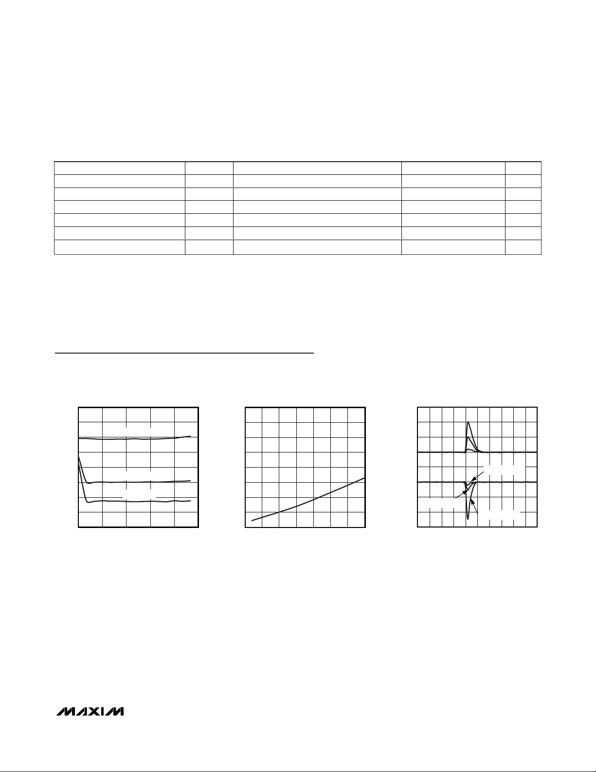
-4
-2
-3
-1
2
3
1
0
4
6 9 12 15 18 21
INPUT OFFSET VOLTAGE DEVIATION
vs. SUPPLY VOLTAGE
MAX9650 toc01
SUPPLY VOLTAGE (V)
INPUT OFFSET VOLTAGE (mV)
TA = +125°C
TA = +25°C
TA = -40°C
0
2
1
4
3
7
6
5
8
-50 0-25 25 50 75 100 125
INPUT OFFSET VOLTAGE DEVIATION
vs. TEMPERATURE
MAX9650 toc02
TEMPERATURE (°C)
INPUT OFFSET VOLTAGE (mV)
I
OUT
(500mA/div)
V
OUT
(125mV/div)
LOAD TRANSIENT
SOURCING
MAX9650 toc05
TIME (1μs/div)
0.1A RESPONSE
1A RESPONSE
0.5A RESPONSE
SYMBOL
MIN TYP MAX
150
100
100
+170
Page 4
MAX9650/MAX9651
High-Current VCOM Drive Op Amps
for TFT LCDs
4 _______________________________________________________________________________________
Typical Operating Characteristics (continued)
(VDD= 19V, GND = 0, VCM= V
OUT
= VDD/2, TA= +25°C, unless otherwise specified.)
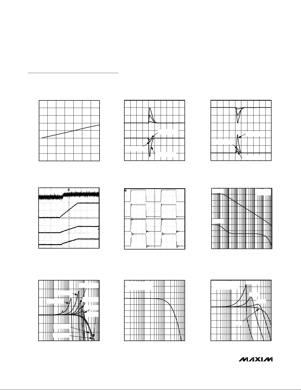
0
2
1
4
3
7
6
5
8
-50 0-25 25 50 75 100 125
SUPPLY CURRENT
vs. TEMPERATURE
MAX9650 toc04
TEMPERATURE (°C)
SUPPLY CURRENT (mA)
I
OUT
(500mA/div)
V
OUT
(125mV/div)
LOAD TRANSIENT
SOURCING
MAX9650 toc05
TIME (1μs/div)
0.1A RESPONSE
1A RESPONSE
0.5A RESPONSE
I
OUT
(500mA/div)
V
OUT
(125mV/div)
LOAD TRANSIENT
SINKING
MAX9650 toc06
TIME (1μs/div)
0.1A RESPONSE
1A RESPONSE
0.5A RESPONSE
100ms/div
STARTUP WAVEFORM
I
DD
10mA/div
V
DD
10V/div
V
IN
5V/div
V
OUT
5V/div
MAX9650 toc07
2μs/div
MAX9650 STEP RESPONSE
WITH VARIOUS C
L
V
OUT
5V/div
V
OUT
5V/div
V
OUT
5V/div
V
OUT
5V/div
MAX9650 toc08
CL = 10pF
CL = 2200pF
CL = 0.01μF
C
L
= 0.022μF
OPEN-LOOP GAIN AND PHASE
vs. FREQUENCY
MAX9650 toc09
FREQUENCY (Hz)
GAIN (dB)
10E+6
1E+6
10E+3
100E+31E+3
100E+0
-60
-40
-20
0
20
40
60
80
100
120
-80
10E+0
100E+6
GAIN
PHASE
CL = 100pF
-180
-120
-60
0
60
120
180
240
300
360
-240
PHASE (DEG)
CLOSED-LOOP SMALL-SIGNAL FREQUENCY
RESPONSE FOR VARIOUS C
L
MAX9650 toc10
FREQUENCY (MHz)
VOLTAGE GAIN (dB)
1010.1
-10
-5
0
5
10
15
20
-15
0.01 100
CL = 0.1μF
CL = 0.01μF
CL = 100pF
CL = 56pF
C
L
= 10pF
CL = 560pF
CL = 0.001μF
C
L
= 0.0022μF
SMALL-SIGNAL GAIN
vs. FREQUENCY
MAX9650 toc11
FREQUENCY (Hz)
GAIN (dB)
10E+61E+6
-6
-5
-4
-3
-2
-1
0
1
2
3
-7
100E+3 100E+6
V
OUT
= 100mV
P-P
RL = 10kΩ TO VDD/2
SMALL-SIGNAL GAIN vs. FREQUENCY
WITH VARIOUS C
L
MAX9650 toc12
FREQUENCY (Hz)
GAIN (dB)
10E+61E+6
-20
-15
-10
-5
0
5
10
15
20
-25
100E+3 100E+6
10,000pF
1000pF
100pF
10pF
V
OUT
= 100mV
P-P
R
L
= 10kΩ TO VDD/2
Page 5

Detailed Description
The MAX9650/MAX9651 operational rail-to-rail
input/output amplifiers hold the VCOM voltage stable
while providing the ability to source and sink a high current quickly (1.3A) into a capacitive load such as the
backplane of a TFT-LCD panel.
Thermal Shutdown
with Temperature Hysteresis
The MAX9650/MAX9651 are capable of high output
currents and feature thermal-shutdown protection with
temperature hysteresis. When the die temperature
reaches +170°C, the device shuts down. When the die
cools down by 15°C, the device turns on again. In a
TFT-LCD application, the duty cycle is very low. Even
with high values of voltage and current, the power dissipation is low and the chip does not shut down.
MAX9650/MAX9651
High-Current VCOM Drive Op Amps
for TFT LCDs
_______________________________________________________________________________________ 5
Pin Description
PIN
MAX9650
µMAX-EP,
MAX9651
FUNCTION
16 1
VCOM Output A
24 4
Ground
33 3
Positive Input A
42 2
Negative Input A
57 8V
DD
Positive-Supply Input. Bypass VDD to GND with a 0.1µF capacitor as close as
possible to the device.
—— 5
Positive Input B
—— 6
Negative Input B
—— 7
VCOM Output B
— 1, 5, 8 —
No Connection. Not internally connected.
—— —EP
Exposed Pad (μMAX and TDFN Only). EP is internally connected to GND. Connect EP
to GND.
IN_+
IN_-
GND
OUT_
V
DD
LCD VCOM LOAD
19V
SUPPLY
V
REF
*10μF and 0.1μF CAPACITORS AS CLOSE AS POSSIBLE TO THE PIN.
**(R
S
= R
GEN
) x C
LCD
x 6 < 2μs, WHERE R
GEN
= GENERATOR SOURCE IMPEDANCE.
MAX9650
*C2 = 0.1μF *C1 = 10μF
19V
SUPPLY
V
OUT_
C
LCD
=
0.1μF
RS =
2.2Ω
**0V TO 2.2V
AT 50kHz
Figure 1. Settling Time Test Circuit
NAME
SOT23
TDFN-EP
(µMAX-EP,
TDFN-EP)
OUTA
GND
INA+
INA-
INB+
INB-
OUTB
N.C.
Page 6

MAX9650/MAX9651
High-Current VCOM Drive Op Amps
for TFT LCDs
6 _______________________________________________________________________________________
Applications Information
Output Load
The MAX9650/MAX9651 are designed to drive capacitive loads. A small value of series resistance improves
the performance of the device to ensure stability and
fast settling with very large or very small capacitive
loads. In many cases, this resistance is already present
due to connection resistance in the wiring and no additional physical resistor is necessary. For minimum
series resistance required for stability with capacitive
loading, see Figure 2.
Power Supplies and Bypass Capacitors
The MAX9650/MAX9651 operate from a 6V to 20V single supply or from ±4.5V to ±10V dual supplies. Proper
supply bypassing ensures stability while driving high
transient loads. The MAX9650/MAX9651 require a minimum 10µF (C1) and 0.1µF (C2) power-supply bypass
capacitors placed as close as possible to the powersupply pin (V
DD
). See Figure 3. For dual-supply operation, use 10µF and 0.1µF bypass capacitors on both
supplies (V
DD
and GND) with each capacitor placed as
close as possible to V
DD
and GND.
Layout and Grounding
The exposed pad on the µMAX®and TDFN packages
provide a low thermal resistance for heat dissipation.
Solder the exposed pad to a ground plane for best
thermal performance. Do not route traces under these
packages. For dual-supply operation, the exposed pad
(EP) can be electrically connected to the negative supply or it can be left unconnected.
IN_+
IN_-
GND
OUT_
V
DD
TFT LCD
TFT-LCD
CAPACITANCE
16V
SUPPLY
V
REF
*10μF and 0.1μF CAPACITORS AS CLOSE AS POSSIBLE TO THE PIN.
**R
S
MAY BE NEEDED FOR SOME APPLICATIONS.
**R
S
MAX9650
*C2 = 0.1μF *C1 = 10μF
19V
SUPPLY
Figure 3. Typical TFT-LCD Backplane Drive Circuit
Figure 2. Minimum Combined ESR/Series/Trace Resistance
Required for Stability of the MAX9650 in Response to
Capacitive Loads
Chip Information
PROCESS: BiCMOS
µMAX is a registered trademark of Maxim Integrated Products, Inc.
2.0
1.8
1.6
1.4
1.2
1.0
0.8
RESISTANCE (Ω)
0.6
0.4
0.2
0
UNSTABLE
-7
10
-6
10
CAPACITANCE (F)
STABLE
-5
10
-4
10
Page 7
MAX9650/MAX9651
High-Current VCOM Drive Op Amps
for TFT LCDs
_______________________________________________________________________________________ 7
GND
INA-INA+
1
5V
DD
OUTA
MAX9650
THIN SOT23
2
34
OUTA
N.C.GND
1
2
87N.C.
V
DD
INA-
INA+
N.C.
μMAX-EP
(TDFN-EP)
μMAX-EP
(TDFN-EP)
3
4
6
5
MAX9650
INB-
INB+
GND
1
2
87V
DD
OUTB
INA-
INA+
OUTA
3
4
6
5
MAX9651
+
+
+
Pin Configurations
Page 8

MAX9650/MAX9651
High-Current VCOM Drive Op Amps
for TFT LCDs
8 _______________________________________________________________________________________
Package Information
For the latest package outline information and land patterns, go to www.maxim-ic.com/packages. Note that a “+”, “#”, or “-” in the
package code indicates RoHS status only. Package drawings may show a different suffix character, but the drawing pertains to the
package regardless of RoHS status.
PACKAGE TYPE PACKAGE CODE OUTLINE NO.
LAND
PATTERN NO.
5 SOT23 Z5+2
21-0113
90-0241
8 µMAX U8E+2
21-0107
90-0145
8 TDFN-EP T833+2
21-0137
90-0058
Page 9

MAX9650/MAX9651
High-Current VCOM Drive Op Amps
for TFT LCDs
_______________________________________________________________________________________ 9
Package Information (continued)
For the latest package outline information and land patterns, go to www.maxim-ic.com/packages. Note that a “+”, “#”, or “-” in the
package code indicates RoHS status only. Package drawings may show a different suffix character, but the drawing pertains to the
package regardless of RoHS status.
Page 10

MAX9650/MAX9651
High-Current VCOM Drive Op Amps
for TFT LCDs
10 ______________________________________________________________________________________
8L, μMAX, EXP PAD.EPS
C
1
1
21-0107
Package Information (continued)
For the latest package outline information and land patterns, go to www.maxim-ic.com/packages. Note that a “+”, “#”, or “-” in the
package code indicates RoHS status only. Package drawings may show a different suffix character, but the drawing pertains to the
package regardless of RoHS status.
Page 11

MAX9650/MAX9651
High-Current VCOM Drive Op Amps
for TFT LCDs
______________________________________________________________________________________ 11
Package Information (continued)
For the latest package outline information and land patterns, go to www.maxim-ic.com/packages. Note that a “+”, “#”, or “-” in the
package code indicates RoHS status only. Package drawings may show a different suffix character, but the drawing pertains to the
package regardless of RoHS status.
Page 12

MAX9650/MAX9651
High-Current VCOM Drive Op Amps
for TFT LCDs
12 ______________________________________________________________________________________
COMMON DIMENSIONS
SYMBOL
MIN. MAX.
A 0.70 0.80
D 2.90 3.10
E 2.90 3.10
A1
0.00 0.05
L0.200.40
PKG. CODE
N
D2
E2 e
JEDEC SPEC
b
[(N/2)-1] x e
PACKAGE VARIATIONS
0.25 MIN.k
A2 0.20 REF.
2.00 REF0.25±0.05
0.50 BSC
2.30±0.1010
T1033-1
2.40 REF0.20±0.05- - - -
0.40 BSC
1.70±0.10 2.30±0.1014
T1433-1
1.50±0.10
MO229 / WEED-3
0.40 BSC
- - - -
0.20±0.05 2.40 REFT1433-2 14 2.30±0.101.70±0.10
T633-2
6 1.50±0.10 2.30±0.10 0.95 BSC MO229 / WEEA 0.40±0.05 1.90 REF
T833-2
8 1.50±0.10 2.30±0.10
0.65 BSC MO229 / WEEC
0.30±0.05 1.95 REF
T833-3
8 1.50±0.10 2.30±0.10
0.65 BSC MO229 / WEEC
0.30±0.05 1.95 REF
2.30±0.10 MO229 / WEED-3 2.00 REF0.25±0.050.50 BSC1.50±0.1010
T1033-2
0.25±0.05 2.00 REF10
0.50 BSC MO229 / WEED-3
2.30±0.101.50±0.10
T1033MK-1
0.40 BSC
- - - - 0.20±0.05 2.40 REFT1433-3F 14 2.30±0.101.70±0.10
Package Information (continued)
For the latest package outline information and land patterns, go to www.maxim-ic.com/packages. Note that a “+”, “#”, or “-” in the
package code indicates RoHS status only. Package drawings may show a different suffix character, but the drawing pertains to the
package regardless of RoHS status.
Page 13

MAX9650/MAX9651
High-Current VCOM Drive Op Amps
for TFT LCDs
Maxim cannot assume responsibility for use of any circuitry other than circuitry entirely embodied in a Maxim product. No circuit patent licenses are
implied. Maxim reserves the right to change the circuitry and specifications without notice at any time.
Maxim Integrated Products, 120 San Gabriel Drive, Sunnyvale, CA 94086 408-737-7600 ____________________
13
© 2010 Maxim Integrated Products Maxim is a registered trademark of Maxim Integrated Products, Inc.
Revision History
REVISION
NUMBER
REVISION
DATE
DESCRIPTION
PAGES
CHANGED
0 7/08 Initial release —
1 10/08 Updated slew rate and added TDFN-EP package 1, 2, 6, 10, 11
2 5/09 Updated continuous output current specification 2
32/10
Added automotive part to Ordering Information, corrected units for input offset
voltage, and added figure for minimum series resistance
1, 2, 5, 6
47/10
Removed extraneous information in the Electrical Characteristics table and
corrected typo in TOC 5
2, 4
 Loading...