

Page 1

EVALUATION KIT AVAILABLE
19-5968; Rev 1; 1/12
MAX9647/MAX9648
General-Purpose, Low-Voltage,
Tiny Pack Comparators
General Description
The MAX9647/MAX9648 comparators are drop-in, pin-forpin compatible replacements for the LMX331/LMX331H.
The MAX9648 has the added benefit of internal hysteresis to provide noise immunity, preventing output oscillations even with slow moving input signals.
Advantages of the ICs include low supply voltage, small
package, and low cost. They also offer a wide supply
voltage range, wide operating temperature range, competitive CMRR and PSRR, response time characteristics,
input offset, low noise, output saturation voltage, input
bias current, and RF immunity.
The ICs are available in both 5-pin SC70 and SOT23
packages.
Applications
Mobile Communications
Notebooks and PDAs
Automotive Applications
Battery-Powered Electronics
General-Purpose Portable Devices
General-Purpose Low-Voltage Applications
Features
S Guaranteed +1.8V to +5.5V Performance
S -40NC to +125NC Automotive Temperature Range
S Low Supply Current (60µA/Channel at
V
= +5.0V)
DD
S Input Common-Mode Voltage Range Includes
Ground
S No Phase Reversal for Overdriven Inputs
S Low Output Saturation Voltage (120mV)
S Internal 2mV Hysteresis (MAX9648)
S 5-Pin SC70 Space-Saving Package
(2.0mm x 2.1mm x 1.0mm)
Ordering Information appears at end of data sheet.
For related parts and recommended products to use with this part,
refer to www.maxim-ic.com/MAX9647.related.
����������������������������������������������������������������� Maxim Integrated Products 1
For pricing, delivery, and ordering information, please contact Maxim Direct at 1-888-629-4642,
or visit Maxim’s website at www.maxim-ic.com.
Page 2
MAX9647/MAX9648
General-Purpose, Low-Voltage,
Tiny Pack Comparators
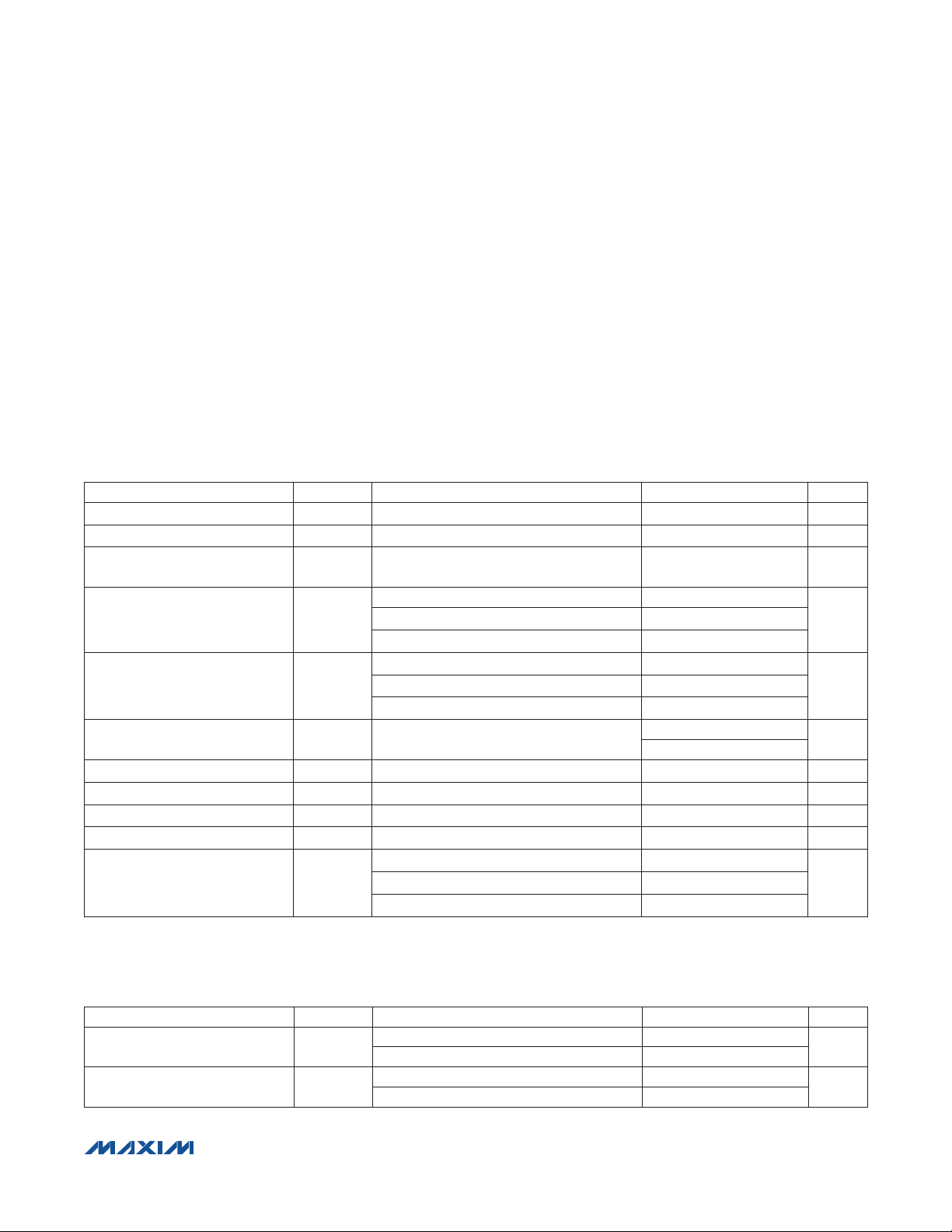
ABSOLUTE MAXIMUM RATINGS
Supply Voltage (VDD to VSS)...................................-0.3V to +6V
All Other Pins ................................. (VSS - 0.3V) to (VDD + 0.3V)
Continuous Power Dissipation (TA = +70NC)
SC70 (derate 3.1 mW/NC above +70NC)......................247mW
SOT23 (derate 7.1 mW/NC above +70NC) ...................571mW
Stresses beyond those listed under “Absolute Maximum Ratings” may cause permanent damage to the device. These are stress ratings only, and functional operation of the device at these or any other conditions beyond those indicated in the operational sections of the specifications is not implied. Exposure to absolute
maximum rating conditions for extended periods may affect device reliability.
DC ELECTRICAL CHARACTERISTICS—2.7V OPERATION
(VDD = 2.7V, VSS = 0V, VCM = 0V, RL = 5.1kI connected to VDD, typical values are at TA = +25NC, unless otherwise noted. Boldface
limits apply at the defined temperature extremes.) (Note 1)
PARAMETER SYMBOL CONDITIONS MIN TYP MAX UNITS
Input Offset Voltage V
Input Voltage Hysteresis V
Input Offset Voltage Average
Temperature Drift
Input Bias Current I
Input Offset Current I
Input Voltage Range V
Voltage Gain A
Output Saturation Voltage V
Output Sink Current I
Supply Current I
Output Leakage Current
HYST
TCV
OS
B
OS
CM
V
SAT
O
S
MAX9648 only 2 mV
OS
TA = +25NC Q0.0003 Q250
TA = -40NC to +85NC
TA = -40NC to +125NC
TA = +25NC Q0.0003 Q50
TA = -40NC to +85NC
TA = -40NC to +125NC
MAX9647 only 500 V/mV
I
P 1mA
SINK
VO P 1.5V
(Note 2) 52 100
TA = +25NC
TA = -40NC to +125NC
Operating Temperature Range ........................ -40NC to +125NC
Junction Temperature .....................................................+150NC
Storage Temperature Range ............................ -65NC to +150NC
Lead Temperature (soldering, 10s) ................................+300NC
Soldering Temperature (reflow) ......................................+260NC
0.4 7 mV
1.5
±400
±400
±150
±150
-0.1
2.0
25 mV
5 16 mA
0.005
FV/NC
nA
nA
V
FA
1
2
FATA = -40NC to +85NC
AC ELECTRICAL CHARACTERISTICS—2.7V OPERATION
(VDD = 2.7V, VSS = 0V, VCM = 0V, RL = 5.1kI connected to VDD, typical values are at TA = +25NC, unless otherwise noted. Boldface
limits apply at the defined temperature extremes.) (Note 1)
PARAMETER SYMBOL CONDITIONS MIN TYP MAX UNITS
Propagation Delay Output
High to Low (Note 3)
Propagation Delay Output
Low to High (Note 3)
����������������������������������������������������������������� Maxim Integrated Products 2
t
PHL
t
PLH
Input overdrive = 10mV 70
Input overdrive = 100mV 50
Input overdrive = 10mV 115
Input overdrive = 100mV 100
ns
ns
Page 3
MAX9647/MAX9648
General-Purpose, Low-Voltage,
Tiny Pack Comparators
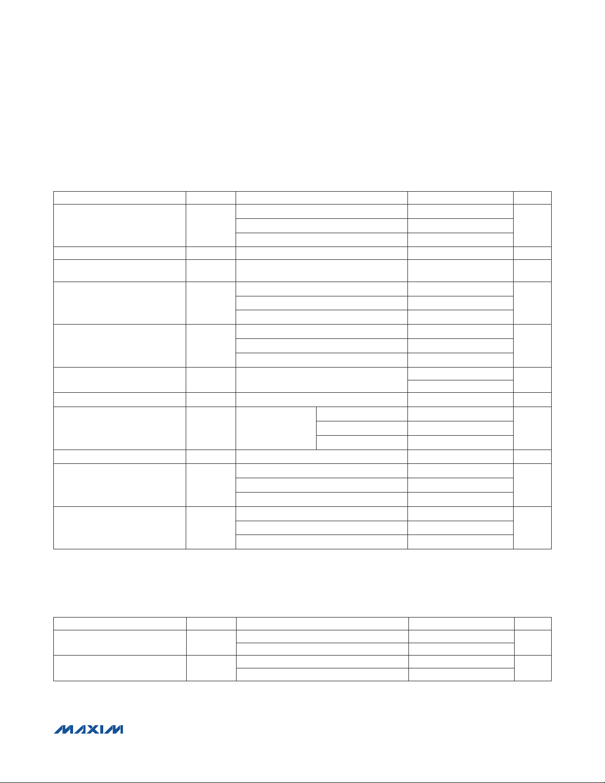
DC ELECTRICAL CHARACTERISTICS–5.0V OPERATION
(VDD = 5V, VSS = 0V, VCM = 0V, RL = 5.1kI connected to VDD, typical values are at TA = +25NC, unless otherwise noted. Boldface
limits apply at the defined temperature extremes.) (Note 1)
PARAMETER SYMBOL CONDITIONS MIN TYP MAX UNITS
TA = +25NC
Input Offset Voltage V
Input Voltage Hysteresis MAX9648 only 2 mV
Input Offset Voltage Average
Temperature Drift
Input Bias Current I
Input Offset Current I
Input Voltage Range V
Voltage Gain A
Output Saturation Voltage V
Output Sink Current I
Supply Current (Note 2) I
Output Leakage Current
OS
TCV
B
OS
CM
SAT
O
S
TA = -40NC to +85NC
TA = -40NC to +125NC
OS
TA = +25NC Q0.007 Q250
TA = -40NC to +85NC
TA = -40NC to +125NC
TA = +25NC Q0.007 Q50
TA = -40NC to +85NC
TA = -40NC to +125NC
MAX9647 only 20 500 V/mV
V
TA = +25NC
I
P 4mA
SINK
VO P 1.5V
TA = +25NC
TA = -40NC to +125NC
TA = +25NC
TA = -40NC to +125NC
TA = -40NC to +85NC
TA = -40NC to +125NC
10 35 mA
0.4 7
1.5
±400
±400
±150
±150
-0.1
4.2
120 400
60 120
0.005
9
9
700
700
150
170
1
2
mV
FV/NC
nA
nA
V
mV
FATA = -40NC to +85NC
FATA = -40NC to +85NC
AC ELECTRICAL CHARACTERISTICS–5.0V OPERATION
(VDD = 5V, VSS = 0V, VCM = 0V, RL = 5.1kI connected to VDD, typical values are at TA = +25NC, unless otherwise noted. Boldface
limits apply at the defined temperature extremes.) (Note 1)
PARAMETER SYMBOL CONDITIONS MIN TYP MAX UNITS
Propagation Delay Output
High to Low (Note 3)
Propagation Delay Output
Low to High (Note 3)
����������������������������������������������������������������� Maxim Integrated Products 3
t
PHL
t
PLH
Input overdrive = 10mV 70
Input overdrive = 100mV 50
Input overdrive = 10mV 110
Input overdrive = 100mV 100
ns
ns
Page 4
MAX9647/MAX9648
General-Purpose, Low-Voltage,
Tiny Pack Comparators
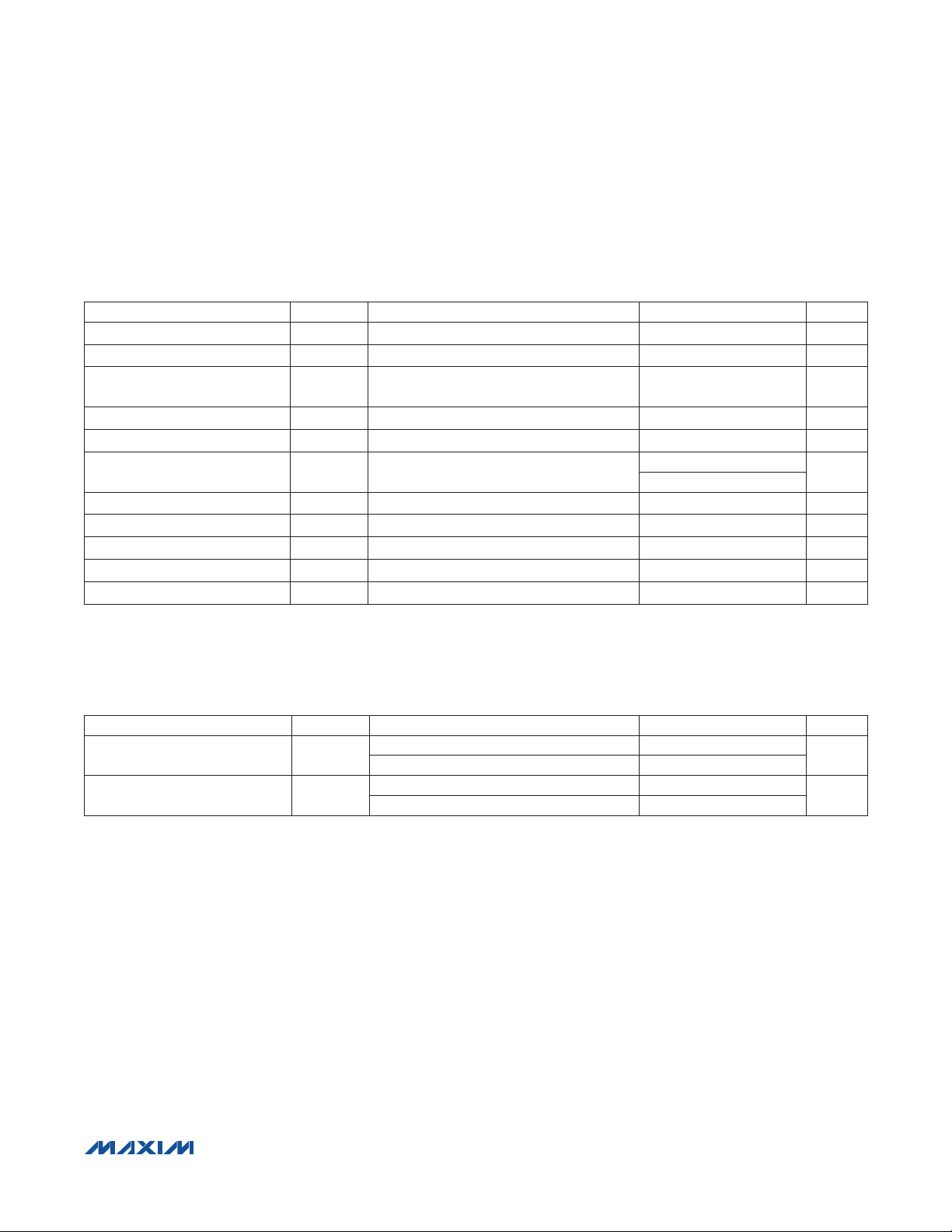
DC ELECTRICAL CHARACTERISTICS—1.8V OPERATION
(VDD = 1.8V, VSS = 0V, VCM = 0V, RL = 5.1kI connected to VDD, typical values are at TA = +25NC, unless otherwise noted. Boldface
limits apply at the defined temperature extremes.) (Note 1)
PARAMETER SYMBOL CONDITIONS MIN TYP MAX UNITS
Input Offset Voltage V
Input Voltage Hysteresis MAX9648 only 2 mV
Input Offset Voltage Average
Temperature Drift
Input Bias Current I
Input Offset Current I
Input Voltage Range V
Output Saturation Voltage V
Power-Supply Rejection Ratio PSRR VDD = 1.8V to 5.5V 60 90 dB
Output Sink Current I
Supply Current I
Output Leakage Current 0.001
TCV
OS
B
OS
CM
SAT
O
S
OS
I
P 1mA
SINK
VO P 1.5V
(Note 2) 50 100
0.4 5 mV
1.5
0.0003 nA
0.0003 nA
-0.1
1
56 mV
6.4 mA
FV/NC
FA
FA
V
AC ELECTRICAL CHARACTERISTICS—1.8V OPERATION
(VDD = 1.8V, VSS = 0V, VCM = 0V, RL = 5.1kI connected to VDD, typical values are at TA = +25NC, unless otherwise noted. Boldface
limits apply at the defined temperature extremes.) (Note 1)
PARAMETER SYMBOL CONDITIONS MIN TYP MAX UNITS
Propagation Delay Output
High to Low (Note 3)
Propagation Delay Output
Low to High (Note 3)
Note 1: All devices are production tested at TA = +25NC. All temperature limits are guaranteed by design.
Note 2: Supply current when output is high.
Note 3: Input overdrive is the overdrive voltage beyond the offset and hysteresis-determined trip points.
t
PHL
t
PLH
Input overdrive = 10mV 70
Input overdrive = 100mV 60
Input overdrive = 10mV 120
Input overdrive = 100mV 110
ns
ns
����������������������������������������������������������������� Maxim Integrated Products 4
Page 5

(V
11
16
DD
= 5V, V
SS
SUPPLY CURRENT (µA)
SUPPLY CURRENT (µA)
INPUT BIAS CURRENT (nA)
= 0V, V
= 0V, RL = 5.1kI, CL = 10pF, overdrive = 100mV, TA = +25NC, unless otherwise noted.)
CM
SUPPLY CURRENT
vs. SUPPLY VOLTAGE
90
80
70
60
50
40
30
20
10
0
1.0 6.0
V
= HIGH
OUT
TA = +125°C
SUPPLY VOLTAGE (V)
TA = +25°C
TA = +85°C
TA = -40°C
SUPPLY CURRENT vs. FREQUENCY
900
800
700
600
500
400
300
200
100
(V
OVERDRIVE
V
= 5V
DD
V
= 2.7V
DD
0
INPUT FREQUENCY (Hz)
= 10mV)
V
= 1.8V
DD
100k10k1k10010
INPUT BIAS CURRENT
vs. TEMPERATURE
0.6
0.5
0.4
0.3
0.2
0.1
V
DD
V
DD
= 2.7V
V
DD
= 1.8V
= 5V
MAX9647/MAX9648
General-Purpose, Low-Voltage,
Tiny Pack Comparators
Typical Operating Characteristics
SUPPLY CURRENT
70
MAX9647 toc01
5.55.04.0 4.52.0 2.5 3.0 3.51.5
MAX9647 toc03
M
MAX9647 toc05
60
50
40
30
SUPPLY CURRENT (µA)
20
10
0
1.2
1.0
0.8
0.6
0.4
INPUT OFFSET VOLTAGE (mV)
0.2
0
-50 125
300
250
200
150
100
OUTPUT VOLTAGE LOW (mV)
50
vs. SUPPLY VOLTAGE
TA = +85°C
TA = +25°C
V
= LOW
OUT
SUPPLY VOLTAGE (V)
INPUT OFFSET VOLTAGE
vs. TEMPERATURE
VDD = 5V
VDD = 2.7V
TEMPERATURE (°C)
OUTPUT VOLTAGE LOW
vs. PULLUP RESISTOR
TA = +125°C
TA = -40°C
VDD = 1.8V
5432
1007550250-25
VOL - V
EE
MAX9647 toc02
MAX9647 toc04
MAX9647 toc06
0
-50 125
TEMPERATURE (°C)
1007550250-25
����������������������������������������������������������������� Maxim Integrated Products 5
0
10k1k100 100k
PULLUP RESISTANCE (I)
Page 6

(V
DD
= 5V, V
SS
= 0V, V
= 0V, RL = 5.1kI, CL = 10pF, overdrive = 100mV, TA = +25NC, unless otherwise noted.)
CM
PROPAGATION DELAY vs. CAPACITIVE LOAD
600
(V
OVERDRIVE
= 100mV)
MAX9647/MAX9648
General-Purpose, Low-Voltage,
Tiny Pack Comparators
Typical Operating Characteristics (continued)
PROPAGATION DELAY vs. TEMPERATURE
(V
120
OVERDRIVE
= 100mV)
500
400
300
200
PROPAGATION DELAY (ns)
100
0
0 100
t
PLH
t
PHL
CAPACITIVE LOAD (pF)
PROPAGATION DELAY
vs. INPUT OVERDRIVE (t
140
130
120
110
100
TA = +125°C
90
80
70
PROPAGATION DELAY (ns)
60
50
40
10 1000
INPUT OVERDRIVE VOLTAGE (mV)
TA = +40°C
TA = +85°C
100
80604020
)
PLH
TA = +25°C
MAX9647 toc07
MAX9647 toc09
100
80
60
40
PROPIGATION DELAY (ns)
20
0
-50 125
t
PLH
t
PHL
TEMPERATURE (°C)
PROPAGATION DELAY
vs. INPUT OVERDRIVE (t
80
75
70
65
60
TA = -40°C
55
50
45
PROPAGATION DELAY (ns)
40
35
30
TA = +25°C
10 1000
INPUT OVERDRIVE VOLTAGE (mV)
TA = +125°C
100
1007550250-25
)
PHL
TA = +85°C
MAX9647 toc08
MAX9647 toc10
INPUT HYSTERESIS VOLTAGE
vs. TEMPERATURE
3.0
2.5
2.0
1.5
1.0
INPUT HYSTERESIS VOLTAGE (mV)
0.5
0
-50 125
VDD = 5V
VDD = 2.7V
VDD = 1.8V
TEMPERATURE (°C)
MAX9647 toc11
V
IN
V
OUT
1007550250-25
PROPAGATION DELAY
100mV OVERDRIVE
100ns/div
MAX9647 toc12
����������������������������������������������������������������� Maxim Integrated Products 6
Page 7

(V
DD
= 5V, V
SS
= 0V, V
MAX9647/MAX9648
General-Purpose, Low-Voltage,
Tiny Pack Comparators
Typical Operating Characteristics (continued)
= 0V, RL = 5.1kI, CL = 10pF, overdrive = 100mV, TA = +25NC, unless otherwise noted.)
CM
PROPAGATION DELAY
10mV OVERDRIVE
V
IN
V
OUT
100ns/div
MAX9647 toc13
V
IN
V
OUT
500kHz RESPONSE
10mV OVERDRIVE
V
IN
MAX9647 toc15
V
IN
500kHz RESPONSE
100mV OVERDRIVE
400ns/div
100kHz RESPONSE
100mV OVERDRIVE
MAX9647 toc14
MAX9647 toc16
V
OUT
400ns/div
V
OUT
2µs/div
100kHz RESPONSE
10mV OVERDRIVE
V
IN
V
OUT
2µs/div
MAX9647 toc17
V
200mV/div
V
2V/div
V
OUT
2V/div
IN+
DD
POWER-UP RESPONSE
4µs/div
MAX9647 toc18
����������������������������������������������������������������� Maxim Integrated Products 7
Page 8

MAX9647/MAX9648
General-Purpose, Low-Voltage,
Tiny Pack Comparators
Pin Configuration
TOP VIEW
+
1IN+
MAX9647
MAX9648
2
V
SS
5V
DD
IN-
3 OUT
PIN NAME FUNCTION
1 IN+ Noninverting Input
2 V
3 IN- Inverting Input
4 OUT Comparator Output (Open Drain)
5 V
SS
DD
Negative Supply (Connect to GND)
Positive Supply
Detailed Description
The MAX9647/MAX9648 are low-cost, general-purpose
comparators that have a single-supply +1.8V to +5V
operating voltage range. The common-mode input range
extends from -0.1V below the negative supply to within
+0.7V of the positive supply. They require approximately
60FA per comparator with a 5V supply and 52FA with a
2.7V supply.
The MAX9648 has 2mV of hysteresis for noise immunity.
This significantly reduces the chance of output oscillations even with slow moving input signals. The ICs are
ideal for automotive applications because they operate from -40NC to +125NC. See the Typical Operating
Characteristics.
4
SC70/SOT23
Pin Description
Applications Information
Hysteresis
Many comparators oscillate in the linear region of operation because of noise or undesired parasitic feedback.
This tends to occur when the voltage on one input is
equal or very close to the voltage on the other input. The
MAX9648 has internal hysteresis to counter parasitic
effects and noise.
The hysteresis in a comparator creates two trip points:
one for the rising input voltage and one for the falling
input voltage (Figure 1). The difference between the trip
points is the hysteresis. When the comparator’s input
voltages are equal, the hysteresis effectively causes
one comparator input to move quickly past the other,
thus taking the input out of the region where oscillation
occurs. This provides clean output transitions for noisy,
slow-moving input signals.
����������������������������������������������������������������� Maxim Integrated Products 8
Page 9

MAX9647/MAX9648
General-Purpose, Low-Voltage,
Tiny Pack Comparators
Additional hysteresis can be generated with two resistors using positive feedback (Figure 2). Use the following
procedure to calculate resistor values:
1) Find output voltage when output is high:
V
OUT(HIGH)
= VDD - I
LOAD
x R
L
2) Find the trip points of the comparator using these
formulas:
VTH = V
VTL = V
+ ((V
REF
REF
OUT(HIGH)
(1 - (R2/(R1 + R2)))
- V
)R2)/(R1 + R2)
REF
where VTH is the threshold voltage at which the comparator switches its output from high to low as V
rises above
IN
the trip point, and VTL is the threshold voltage at which
the comparator switches its output from low to high as
V
drops below the trip point.
IN
3) The hysteresis band is:
V
= V
HYST
In this example, let VDD = 5V, V
- VTL = VDD(R2/(R1 + R2))
TH
= 2.5V, I
REF
LOAD
=
50nA, and RL = 5.1kI.
V
OUT(HIGH)
= 5.0V - (50 x 10-9 x 5.1 x 103I) ≈ 5.0V
V
= 2.5 + 2.5(R2/(R1 + R2))
TH
VTL = 2.5(1 - (R2/(R1 + R2)))
Select R2. In this example, choose 1kI.
Select V
. In this example, choose 50mV.
HYST
Solve for R1.
V
HYST
= V
OUT(HIGH)
(R2/(R1 + R2))V
0.050V = 5(1000/(R1 + 1000))V
where R1 ≈ 100kI, VTH = 2.525V, and VTL = 2.475V
Choose R1 and R2 to be large enough as not to exceed
the amount of current the reference can supply.
The source current required is V
The sink current is (V
OUT(HIGH)
/(R1 + R2).
REF
- V
REF
) x (R1 + R2).
Choose RL to be large enough to avoid drawing excess
current, yet small enough to supply the necessary current to drive the load. RL should be between 1kI and
10kI. Choose R1 to be much larger than RL to avoid
lowering V
OUT(HIGH)
ir raising V
OUT(LOW)
.
Board Layout and Bypassing
Use 0.1FF bypass capacitors from VDD to VSS. To maximize performance, minimize stray inductance by putting
this capacitor close to the VDD pin and reducing trace
lengths. For slow moving input signals (rise time > 1ms),
use a 1nF capacitor between IN+ and IN- to reduce high
frequency noise.
IN+
IN-
V
HYST
OUT
Figure 1. Threshold Hysteresis Band (Not to Scale)
����������������������������������������������������������������� Maxim Integrated Products 9
THRESHOLDS
HYSTERESIS
BAND
V
DD
R1
V
V
TH
V
TL
V
Figure 2. Adding Hysteresis with External Resistors
REF
V
R2
IN
IN+
IN-
DD
V
SS
R
L
MAX9647
OUT
V
OUT
Page 10

MAX9647/MAX9648
General-Purpose, Low-Voltage,
Tiny Pack Comparators
Chip Information
PROCESS: BiCMOS
Ordering Information
PART
MAX9647AXK+T
MAX9647AUK+T
MAX9648AXK+T
MAX9648AUK+T
+Denotes a lead(Pb)-free/RoHS-compliant package.
T = Tape and reel.
TEMP
RANGE
-40NC to
+125NC
-40NC to
+125NC
-40NC to
+125NC
-40NC to
+125NC
PINPACKAGE
5 SC70 +AUS
5 SOT23 +AFLM
5 SC70 +AUT
5 SOT23 +AFLN
TOP
MARK
Package Information
For the latest package outline information and land patterns
(footprints), go to www.maxim-ic.com/packages. Note that a
“+”, “#”, or “-” in the package code indicates RoHS status only.
Package drawings may show a different suffix character, but
the drawing pertains to the package regardless of RoHS status.
PACKAGE
TYPE
5 SC70 X5+1
5 SOT23 U5+1
PACKAGE
CODE
OUTLINE
NO.
21-0076 90-0188
21-0057 90-0174
LAND
PATTERN NO.
���������������������������������������������������������������� Maxim Integrated Products 10
Page 11

MAX9647/MAX9648
General-Purpose, Low-Voltage,
Tiny Pack Comparators
Revision History
REVISION
NUMBER
0 10/11 Initial release —
1 1/12 Revised the Typical Operating Characteristics. 6
REVISION
DATE
DESCRIPTION
PAGES
CHANGED
Maxim cannot assume responsibility for use of any circuitry other than circuitry entirely embodied in a Maxim product. No circuit patent licenses are implied.
Maxim reserves the right to change the circuitry and specifications without notice at any time. The parametric values (min and max limits) shown in the Electrical
Characteristics table are guaranteed. Other parametric values quoted in this data sheet are provided for guidance.
Maxim Integrated Products, 120 San Gabriel Drive, Sunnyvale, CA 94086 408-737-7600 11
©
2012 Maxim Integrated Products Maxim is a registered trademark of Maxim Integrated Products, Inc.
 Loading...