

Page 1
19-5228; Rev 2; 1/11
EVALUATION KIT
AVAILABLE
3V/5V Low-Power, Low-Noise, CMOS,
General Description
The MAX9636/MAX9637/MAX9638 are single-supply,
CMOS input op amps featuring wide bandwidth at low
quiescent current, making them suitable for a broad
range of battery-powered applications such as portable
medical instruments, portable media players, and smoke
detectors. A combination of extremely low input bias
currents, low input current noise and low input voltage
noise allows interface to high-impedance sources such
as photodiode and piezoelectric sensors. These devices
are also ideal for general-purpose signal processing
functions such as filtering and amplification in a broad
range of portable, battery-powered applications.
The ICs feature a maximized ratio of gain bandwidth
(GBW) to supply current. The devices operate from a
single 2.1V to 5.5V supply at a typical quiescent supply
current of 36µA. For additional power conservation, the
MAX9636 and MAX9638 offer a low-power shutdown
mode that reduces supply current to 1µA and places the
amplifiers’ outputs into a high-impedance state.
The ICs are specified over the automotive operating temperature range (-40°C to +125°C). The single is offered
in a space-saving, 6-pin SC70 package, while the dual is
offered in tiny, 8-pin SC70 and 10-pin UTQFN packages.
Rail-to-Rail I/O Op Amps
MAX9636/MAX9637/MAX9638
Features
S Low Input Voltage-Noise Density: 38nV/√Hz
S Low Input Current-Noise Density: 0.9fA/√Hz
S Ultra-Low 0.1pA Bias Current
S Low 36µA Quiescent Current
S 1µA Quiescent Current in Shutdown
S Wide 1.5MHz Bandwidth
S Single-Supply Operation VDD = 2.1V to 5.5V
S Available in Tiny 6-Pin SC70, 8-Pin SC70, and
10-Pin UTQFN Packages
S -40°C to +125°C Operating Temperature Range
Ordering Information
PART TEMP RANGE PIN-PACKAGE
MAX9636AXT+ -40NC to +125NC 6 SC70
MAX9637AXA+ -40NC to +125NC 8 SC70
MAX9638AVB+ -40NC to +125NC 10 UTQFN
+Denotes a lead(Pb)-free/RoHS-compliant package.
T = Tape and reel.
Applications
Portable Medical Instruments
Piezoelectric Transducer Amplifiers
Smoke Detectors
Battery-Powered Devices
General-Purpose Signal Conditioning
Notebooks
Portable Media Players
_______________________________________________________________ Maxim Integrated Products 1
For pricing, delivery, and ordering information, please contact Maxim Direct at 1-888-629-4642,
or visit Maxim’s website at www.maxim-ic.com.
Page 2
3V/5V Low-Power, Low-Noise, CMOS,
Rail-to-Rail I/O Op Amps
ABSOLUTE MAXIMUM RATINGS
VDD, SHDN to VSS ..................................................-0.3V to +6V
IN+, IN-, OUT ....................................GND - 0.3V to VDD + 0.3V
Continuous Input Current (any pins) ............................... Q20mA
Output Short Circuit to VDD or VSS Duration .......................... 5s
Thermal Limits (Note 1)
Multiple Layer PCB
Continuous Power Dissipation (TA = +70NC)
6-Pin SC70 (derate 3.1mW/°C above +70NC) ............245mW
BJA ....................................................................... 326.5°C/W
BJC .........................................................................115°C/W
Note 1: Package thermal resistances were obtained using the method described in JEDEC specification JESD51-7, using a four-
layer board. For detailed information on package thermal considerations, refer to www.maxim-ic.com/thermal-tutorial.
Stresses beyond those listed under “Absolute Maximum Ratings” may cause permanent damage to the device. These are stress ratings only, and functional
operation of the device at these or any other conditions beyond those indicated in the operational sections of the specifications is not implied. Exposure to absolute
maximum rating conditions for extended periods may affect device reliability.
ELECTRICAL CHARACTERISTICS
(VDD = 3.3V, VSS = 0V, V
at TA = +25NC, unless otherwise noted.) (Note 2)
PARAMETER SYMBOL CONDITIONS MIN TYP MAX UNITS
DC CHARACTERISTICS
Input Voltage Range V
MAX9636/MAX9637/MAX9638
Input Offset Voltage V
Input Offset Voltage Drift
(Note 3)
Input Bias Current (Note 3) I
Common-Mode Rejection Ratio CMRR
Open-Loop Gain A
Output Short-Circuit Current I
Output Voltage Low V
Output Voltage High V
Output Leakage in Shutdown
IN+
= V
= VCM = VDD/2, RL = 10kI to VDD/2, SHDN = VDD, TA = -40NC to +125NC. Typical values are
IN-
, V
IN+
OS
TCV
OL
SC
OL
OH
Guaranteed by CMRR
IN-
TA = +25NC 0.01 2.2
TA = -40NC to +125NC 3.5
MAX9636 only 7
OS
MAX9637, MAX9638 only 10
TA = +25NC ±0.1 ±0.8
TA = -40NC to +85NC ±50
B
TA = -40NC to +125NC ±800
VSS < VCM <
(VDD - 1.4V)
(VSS - 0.1V) < VCM < (VDD + 0.1V) 58 77
V
= 0.25V from rails 104 124
OUT
V
= 0.4V from rails, RL = 600I 100 120
OUT
Short to VDD 55
Short to VSS 40
V
OUT
VDD - V
OUT
SHDN = VSS, V
MAX9638 only)
8-Pin SC70 (derate 3.1mW/NC above +70NC) .............245mW
BJA ......................................................................... 326°C/W
BJC .........................................................................115NC/W
10-Pin UTQFN (derate 7mW/NC above +70NC) ........558.7mW
BJA ...................................................................... 143.2NC/W
BJC .........................................................................20.1NC/W
Operating Temperature Range ........................ -40NC to +125NC
Junction Temperature ....................................................+150NC
Lead Temperature (soldering 10s) .................................+300NC
Soldering Temperature (reflow) ......................................+260NC
V
-
SS
0.1
TA = +25NC 72 86
TA = -40NC to +125NC 68
RL = 10kI 0.014 0.03
RL = 600I 0.044 0.08
RL = 10kI 0.019 0.04
RL = 600I 0.057 0.1
OUT
= 0V to V
(MAX9636,
DD
0.01 1 FA
V
+
DD
0.1
V
mV
FV/NC
pA
dB
dB
mA
V
V
2
Page 3
3V/5V Low-Power, Low-Noise, CMOS,
Rail-to-Rail I/O Op Amps
ELECTRICAL CHARACTERISTICS (continued)
(VDD = 3.3V, VSS = 0V, V
at TA = +25NC, unless otherwise noted.) (Note 2)
PARAMETER SYMBOL CONDITIONS MIN TYP MAX UNITS
AC CHARACTERISTICS
Input Voltage Noise Density e
Input Voltage Noise 0.1Hz ≤ f ≤ 10Hz 5 FV
Input Current Noise Density I
Input Capacitance C
Gain Bandwidth GBW 1.5 MHz
Slew Rate SR 0.9 V/Fs
Capacitive Loading C
Distortion THD
Settling Time To 0.1%, V
Crosstalk
POWER-SUPPLY CHARACTERISTICS
Power-Supply Range V
Power-Supply Rejection Ratio PSRR
Quiescent Current I
Shutdown Supply Current I
Shutdown Input V
Shutdown Input V
Shutdown Input Bias Current
(Note 3)
Turn-On Time t
Power-Up Time t
Note 2: All devices are 100% production tested at TA = +25NC. Temperature limits are guaranteed by design.
Note 3: Parameter is guaranteed by design.
IN+
= V
= VCM = VDD/2, RL = 10kI to VDD/2, SHDN = VDD, TA = -40NC to +125NC. Typical values are
IN-
f = 1kHz 38 nV/√Hz
N
f = 1kHz 0.9 fA/√Hz
N
IN
LOAD
DD
DD
DD_SHDNVSHDN
I
SHDN
ON
UP
No sustained oscillations 300 pF
f = 10kHz, VO = 2V
f = 10kHz, VO = 2V
VDD = 5.5V
f = 1kHz (MAX9637, MAX9638) 100
f = 10kHz (MAX9637, MAX9638) 80
Guaranteed by PSRR 2.1 5.5 V
V
IN+
VDD - VSS = 2.1V
to 5.5V
Per amplifier
Over the power-supply range (MAX9636,
IL
MAX9638 only)
Over the power-supply range (MAX9636,
IH
MAX9638 only)
MAX9636, MAX9638 only 1 100 nA
V
SHDN
only)
VDD = 0V to 3.3V 18 Fs
, AV = 1V/V -68
P-P
, AV = 1V/V,
P-P
= 2V step, AV = 1V/V 11.5 Fs
OUT
= V
= VSS,
IN-
P V
(MAX9636, MAX9638 only) 1 FA
IL
= 0V to 3V (MAX9636, MAX9638
TA = +25NC 72 100
TA = -40NC to +125NC 69
TA = +25NC 36 55
TA = -40NC to +125NC 60
1.4 V
2 pF
-74
0.5 V
60 Fs
dB
dB
dB
FA
MAX9636/MAX9637/MAX9638
P-P
3
Page 4
3V/5V Low-Power, Low-Noise, CMOS,
OUTPUT VOLTAGE HIGH (mV)
Rail-to-Rail I/O Op Amps
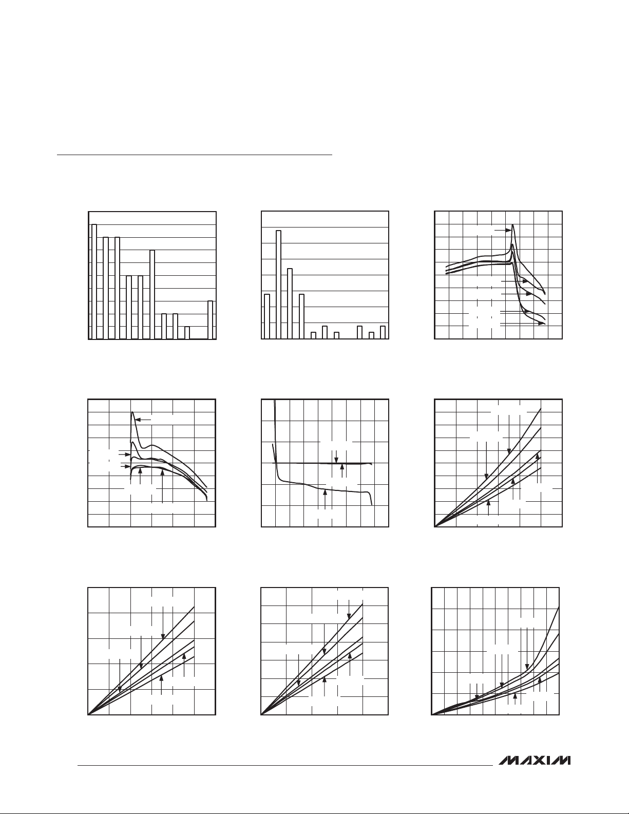
Typical Operating Characteristics
(VDD = 3.3V, VSS = 0V, V
TA = +25NC, unless otherwise noted.)
OFFSET VOLTAGE HISTOGRAM
20
18
16
14
12
10
8
6
PERCENT OCCURANCE (%)
4
2
0
OFFSET VOLTAGE (mV)
IN+
= V
= VCM = VDD/2, RL = 10kI to VDD/2, SHDN = VDD, TA = -40NC to +125NC. Typical values are at
IN-
OFFSET VOLTAGE THERMAL
COEFFICIENT HYSTOGRAM
40
35
MAX9636 toc01
30
25
20
15
PERCENT OCCURANCE (%)
10
5
0
0.90.7 1.00.80.1 0.2 0.3 0.4 0.5 0.60
0
OFFSET VOLTAGE THERMAL COEFFICIENT (µV/°C)
1.00.1 0.2 0.3 0.5 0.70.6 0.80.4 0.9
500
450
MAX9636 toc02
400
350
300
250
200
OFFSET VOLTAGE (µV)
150
100
50
0
INPUT OFFSET VOLTAGE
vs. COMMON-MODE VOLTAGE
TA = -40°C
TA = 0°C
TA = +25°C
TA = +85°C
TA = +125°C
-0.5
COMMON-MODE VOLTAGE (V)
3.53.02.0 2.50.5 1.0 1.50
4.0
MAX9636 toc03
INPUT OFFSET VOLTAGE
vs. SUPPLY VOLTAGE V
400
380
360
340
320
MAX9636/MAX9637/MAX9638
TA = 0°C
300
TA = +25°C
280
OFFSET VOLTAGE (µV)
260
240
220
200
0 6
TA = +85°C
TA = +125°C
SUPPLY VOLTAGE (V)
OUTPUT VOLTAGE LOW vs. SINK CURRENT
= 3.3V
V
250
200
150
100
OUTPUT VOLTAGE LOW (mV)
TA = +25°C
50
0
0 12
DD
T
A
TA = +85°C
TA = -40°C
SINK CURRENT (mA)
CM
TA = -40°C
= +125°C
= VDD/2
TA = 0°C
600
400
MAX9636 toc04
200
0
-200
INPUT BIAS CURRENT (pA)
-400
54321
-600
-0.5 4.0
OUTPUT VOLTAGE LOW vs. SINK CURRENT
350
300
MAX9636 toc07
250
200
150
100
OUTPUT VOLTAGE LOW (mV)
50
108642
0
INPUT BIAS CURRENT
vs. COMMON-MODE VOLTAGE
TA = +25°C
TA = +85°C
TA = +125°C
COMMON-MODE VOLTAGE (V)
VDD = 5V
TA = +125°C
TA = +85°C
TA = +25°C
TA = 0°C
TA = -40°C
0 25
SINK CURRENT (mA)
OUTPUT VOLTAGE LOW vs. SINK CURRENT
= 2.1V
V
500
450
MAX9636 toc05
400
350
300
250
200
150
OUTPUT VOLTAGE LOW (mV)
100
50
3.53.02.52.01.51.00.50
0
0 12
DD
TA = +125°C
MAX9636 toc06
TA = +85°C
TA = +25°C
TA = 0°C
TA = -40°C
108642
SINK CURRENT (mA)
OUTPUT VOLTAGE HIGH vs. SOURCE CURRENT
= 2.1V, VOH = VDD - V
V
1200
1000
MAX9636 toc08
800
600
400
200
2015105
DD
TA = +85°C
TA = +25°C
0
0 10
SOURCE CURRENT (mA)
TA = -40°C
OUT
MAX9636 toc09
TA = +125°C
TA = 0°C
987654321
4
Page 5

3V/5V Low-Power, Low-Noise, CMOS,
OUTPUT VOLTAGE HIGH (mV)
OPEN-LOOP GAIN (dB)
Rail-to-Rail I/O Op Amps
Typical Operating Characteristics (continued)
(VDD = 3.3V, VSS = 0V, V
TA = +25NC, unless otherwise noted.)
OUTPUT VOLTAGE HIGH vs. SOURCE CURRENT
= 3.3V, VOH = VDD - V
V
2000
1800
1600
1400
1200
1000
800
600
OUTPUT VOLTAGE HIGH (mV)
400
200
DD
TA = +85°C
TA = +25°C
0
0 35
SOURCE CURRENT (mA)
IN+
TA = +125°C
TA = -40°C
= V
= VCM = VDD/2, RL = 10kI to VDD/2, SHDN = VDD, TA = -40NC to +125NC. Typical values are at
IN-
OUTPUT VOLTAGE HIGH vs. SOURCE CURRENT
OUT
TA = 0°C
302515 20105
MAX9636 toc10
1200
1000
800
600
400
200
= 5V, VOH = VDD - V
V
DD
TA = +85°C
TA = +25°C
TA = 0°C
0
SOURCE CURRENT (mA)
OUT
TA = +125°C
TA = -40°C
MAX9636 toc11
454035302520151050 50
SUPPLY CURRENT vs. SUPPLY VOLTAGE
45
43
TA = +85°C
41
39
37
35
33
31
SUPPLY CURRENT (µA)
29
TA = -40°C
27
25
2.0 6.0
TA = +125°C
TA = +25°C
TA = 0°C
SUPPLY VOLTAGE (V)
PER AMPLIFIER
5.55.04.0 4.53.0 3.52.5
MAX9636/MAX9637/MAX9638
MAX9636 toc12
140
120
100
80
60
40
20
0
-20
-40
-60
0.001 10,000
100
90
80
70
60
50
40
30
20
POWER-SUPPLY REJECTION RATIO (dB)
10
0
0.01 10,000
OPEN-LOOP GAIN AND PHASE
vs. FREQUENCY
GAIN
PHASE
FREQUENCY (kHz)
1001 100.10.01
MAX9636 toc13
1000
POWER-SUPPLY REJECTION RATIO
vs. FREQUENCY
10001001010.1
FREQUENCY (kHz)
180
135
90
45
0
-45
-90
-135
-180
MAX9636 toc16
COMMON-MODE REJECTION RATIO
vs. FREQUENCY
0
-10
-20
-30
-40
-50
CMRR (dB)
PHASE (DEG)
-60
-70
-80
-90
0.01 10,000
FREQUENCY (kHz)
DC POWER-SUPPLY REJECTION RATIO
vs. TEMPERATURE
100
98
96
94
92
90
88
86
84
82
DC POWER-SUPPLY REJECTION RATIO (dB)
80
-50 125
TEMPERATURE (°C)
DC COMMON-MODE REJECTION RATIO
vs. TEMPERATURE
100
98
MAX9636 toc14
96
94
92
90
88
86
84
82
DC COMMON-MODE REJECTION RATIO (dB)
10001001010.1
80
-50 125
TEMPERATURE (°C)
MAX9636 toc15
1007525 500-25
INPUT VOLTAGE NOISE vs. FREQUENCY
300
250
MAX9636 toc17
200
150
100
INPUT VOLTAGE NOISE (nV/√Hz)
50
0
1007525 500-25
0.01 100
FREQUENCY (kHz)
1010.1
MAX9636 toc18
5
Page 6

3V/5V Low-Power, Low-Noise, CMOS,
Rail-to-Rail I/O Op Amps
Typical Operating Characteristics (continued)
(VDD = 3.3V, VSS = 0V, V
TA = +25NC, unless otherwise noted.)
IN+
= V
= VCM = VDD/2, RL = 10kI to VDD/2, SHDN = VDD, TA = -40NC to +125NC. Typical values are at
IN-
INPUT CURRENT NOISE vs. FREQUENCY
10
9
8
7
6
5
4
3
INPUT CURRENT NOISE (fA/√Hz)
2
1
0
0.1 1000
FREQUENCY (Hz)
100101
MAX9636 toc19
TOTAL HARMONIC DISTORTION vs.
INPUT VOLTAGE AMPLITUDE
VDD = 5.5V, AO = 1V/V
0
-10
-20
MAX9636/MAX9637/MAX9638
-30
-40
-50
-60
-70
TOTAL HARMONIC DISTORTION (dB)
-80
-90
0 6
INPUT VOLTAGE AMPLITUDE (V
P-P
MAX9636 toc21
54321
)
0.1Hz TO 10Hz VOLTAGE vs. TIME
5µV
NOISE
P-P
2µV/div
10s/div
TOTAL HARMONIC DISTORTION vs.
FREQUENCY V
V
= 2V
OUT
0
-20
-40
-60
-80
TOTAL HARMONIC DISTORTION (dB)
-100
-120
0.01 100
= 5.5V, AO = 1V/V,
DD
, RL = 10kI to VDD/2
P-P
FREQUENCY (kHz)
MAX9636 toc20
MAX9636 toc22
1010.1
LARGE-SIGNAL TRANSIENT RESPONSE
V
IN
2V/div
V
OUT
2µs/div
MAX9636 toc24
V
100mV/div
V
OUT
20mV/div
SMALL-SIGNAL TRANSIENT RESPONSE
IN
1µs/div
MAX9636 toc23
500mV/div
6
Page 7

3V/5V Low-Power, Low-Noise, CMOS,
Rail-to-Rail I/O Op Amps
Typical Operating Characteristics (continued)
(VDD = 3.3V, VSS = 0V, V
TA = +25NC, unless otherwise noted.)
30
25
20
15
10
5
PERCENT OVERSHOOT (%)
0
-5
= V
IN+
= VCM = VDD/2, RL = 10kI to VDD/2, SHDN = VDD, TA = -40NC to +125NC. Typical values are at
IN-
PERCENT OVERSHOOT vs. RESISTIVE LOAD
C
C
LOAD
LOAD
= 100pF
= 50pF
100,00010,0001000100
C
= 300pF
LOAD
10 1,000,000
RESISTIVE LOAD (I)
MAX9636 toc25
STABILITY vs. CAPACITIVE AND RESISTIVE
LOAD R
100
90
80
70
60
50
40
RESISTIVE LOAD (I)
30
20
10
0
100 100,000
IN SERIES WITH C
ISO
STABLE
UNSTABLE
10,0001000
CAPACITIVE LOAD (pF)
LOAD
MAX9636 toc26
MAX9636/MAX9637/MAX9638
STABILITY vs. CAPACITIVE AND RESISTIVE LOAD
IN PARALLEL WITH C
R
100
90
80
70
60
50
40
RESISTIVE LOAD (kI)
30
20
10
0
100 10,000
P
STABLE
CAPACITIVE LOAD (pF)
UNSTABLE
1000
L
SHDN
2V/div
MAX9636 toc27
2V/div
500mV/div
TURN-ON TIME
POWER-UP TIME
V
DD
V
OUT
40µs/div
MAX9636 toc29
MAX9636 toc28
V
OUT
500mV/div
100µs/div
7
Page 8

3V/5V Low-Power, Low-Noise, CMOS,
Rail-to-Rail I/O Op Amps
Pin Configurations
TOP VIEW
+
IN+
1 6
MAX9636
V
SS
2
V
DD
SHDN
5
OUTA
INA+
+
1
2
3
87V
6
DD
OUTBINA-
INB-
IN-
3 4
SC70
OUTA
INA-
OUTB
OUT
8
9
10
+
SHDNB6SHDNA
7
MAX9638
1 2
VDDINB+
4
SS
MAX9637
SC70
5
V
SS
4
INA+
INB-
3
INB+V
5
UTQFN
MAX9636/MAX9637/MAX9638
Pin Description
PIN
MAX9636
(6 SC70)
MAX9637
(8 SC70)
MAX9638
(10 UTQFN)
1 — — IN+ Positive Input
— 3 4 INA+ Positive Input A
— 5 2 INB+ Positive Input B
2 4 5 V
3 — — IN- Negative Input
— 2 9 INA- Negative Input A
— 6 3 INB- Negative Input B
4 — — OUT Output
— 1 8 OUTA Output A
— 7 10 OUTB Output B
— — 6
— — 7
5 — —
6 8 1 V
NAME FUNCTION
SS
SHDNA
SHDNB
SHDN
DD
Negative Power Supply. Bypass with a 0.1FF capacitor to ground.
Active-Low Shutdown A
Active-Low Shutdown B
Active-Low Shutdown
Positive Power Supply. Bypass with a 0.1FF capacitor to ground.
8
Page 9

3V/5V Low-Power, Low-Noise, CMOS,
Detailed Description
The MAX9636/MAX9637/MAX9638 are single-supply,
CMOS input op amps. They feature wide bandwidth at
low quiescent current, making them suitable for a broad
range of battery-powered applications such as portable medical instruments, portable media players, and
smoke detectors. A combination of extremely low input
bias currents, low input current noise, and low input voltage noise allows interface to high-impedance sources
such as photodiode and piezoelectric sensors. These
devices are also ideal for general-purpose signal processing functions such as filtering and amplification in a
broad range of portable, battery-powered applications.
The devices’ operational common-mode range extends
0.1V beyond the supply rails, allowing for a wide variety
of single-supply applications.
The ICs also feature low quiescent current and a shutdown mode that greatly reduces quiescent current while
the device is not operational. This makes the device suitable for portable applications where power consumption
must be minimized.
Rail-to-Rail Input Stage
The operational amplifiers have parallel-connected nand p-channel differential input stages that combine
to accept a common-mode range extending 100mV
beyond the supply rails. The n-channel stage is active
for common-mode input voltages typically greater than
(VDD - 1.2V), and the p-channel stage is active for common-mode input voltages typically less than (VDD - 1.4V).
A small transition region exists, typically VDD - 1.4 to VDD
- 1.2V, during which both pairs are on.
Rail-to-Rail I/O Op Amps
Rail-to-Rail Output Stage
The maximum output voltage swing is load dependent.
However, it is guaranteed to be within 100mV of the
positive rail even with 3mA of load current. To maximize
the output current sourcing capability, these parts do
not come with built-in short-circuit protection. If loads
heavier than 600ω must be driven, then ensure that the
maximum allowable power dissipation is not exceeded
(see the Absolute Maximum Ratings section).
Low Input Bias Current
This op-amp family features ultra-low 0.1pA (typ) input
bias current and guaranteed maximum current of Q50pA
over -40NC to +85NC when the input common-mode voltage is at midrail. For the -40NC to +85NC temperature
range, the variation in the input bias current is small
with changes in the input voltage due to very high input
impedance (in the order of 100GI).
Power-Up Time
The ICs typically require a power-up time of 18µs.
Supply settling time depends on the supply voltage,
the value of the bypass capacitor, the output impedance of the incoming supply, and any lead resistance or
inductance between components. Op amp settling time
depends primarily on the output voltage and is slew-rate
limited. The output settles in approximately 11.5µs for
VDD = 3V and V
graph in the Typical Operating Characteristics section).
= VDD/2V (see the Power-Up Time
OUT
MAX9636/MAX9637/MAX9638
9
Page 10

3V/5V Low-Power, Low-Noise, CMOS,
Rail-to-Rail I/O Op Amps
Driving Capacitive Loads
The ICs have a high tolerance for capacitive loads.
In unity-gain configuration, the op amps can typically
drive up to 300pF pure capacitive load. Increasing the
gain enhances the amplifier’s ability to drive greater
capacitive loads. In unity-gain configurations, capacitive
load drive can be improved by inserting a small (5I to
30I) isolation resistor, R
, in series with the output,
ISO
as shown in Figure 1. This significantly reduces ringing
while maintaining DC performance for purely capacitive loads. However, if the load also has a resistive
component then a voltage-divider is created, introducing a direct current (DC) error at the output. The error
introduced is proportional to the ratio RISO/RL, which
is usually negligible in most cases. Applications that
cannot tolerate this slight DC error can use an alternative approach of providing stability by placing a suitable
resistance in parallel with the capacitive load as shown
in Figure 2 (see the Typical Operating Characteristics
section for graphs of the stable operating region for
various capacitive loads vs. resistive loads). While this
approach of adding a resistor parallel to the load does
not introduce DC error, it nevertheless reduces the output swing proportionally.
High-Impedance
Sensor Front-Ends
The ICs interface to both current-output sensors, such
as photodiodes (Figure 3), and high-impedance voltage
sources, such as piezoelectric sensors. For currentoutput sensors, a transimpedance amplifier is the most
noise-efficient method for converting the input signal to
a voltage. High-value feedback resistors are commonly
chosen to create large gains, while feedback capacitors
help stabilize the amplifier by cancelling any poles introduced in the feedback function by the highly capacitive
sensor or cabling. A combination of low-current noise
and low-voltage noise is important for these applications.
Take care to calibrate out photodiode dark current if DC
accuracy is important. The high bandwidth and slew
rate also allows AC signal processing in certain medical
photodiode sensor applications such as pulse oximetry.
For voltage-output sensors, a noninverting amplifier is
typically used to buffer and/or apply a small gain to the
input voltage signal. Due to the extremely high impedance of the sensor output, a low input bias current with
minimal temperature variation is very important for these
applications.
MAX9636/MAX9637/MAX9638
-
R
MAX9636/
MAX9637/
MAX9638
+
Figure 1. Using a Series Resistor to Isolate the Capacitive
Load from the Op Amp
Figure 3. The MAX9636 in a Sensor Preamp Configuration
AV =
R
RL + R
PHOTODIODE
ISO
R
C
L
L
≈ 1V/V
ISO
REF
L
V
IN-
MAX9636
IN+
Figure 2. Using a Parallel Resistor to Degenerate the Effect of
the Capacitive Load and Increase Stability
DD
OUT
-
MAX9636/
MAX9637/
MAX9638
+
SIGNAL
CONDITIONING/
FILTERS
MAX1286
ADC
R
R
P
C
L
L
10
Page 11

3V/5V Low-Power, Low-Noise, CMOS,
For best performance, follow standard high-impedance
layout techniques, which include the following:
U Using shielding techniques to guard against parasitic
leakage paths. For example, put a trace connected to
the noninverting input around the inverting input.
U Minimizing the amount of stray capacitance connect-
ed to op amp’s inputs to improve stability. To achieve
this, minimize trace lengths and resistor leads by
placing external components as close as possible to
the package.
U Use separate analog and digital power supplies.
Applications Information
Shutdown Operation
The MAX9636/MAX9638 feature an active-low shutdown
mode that sends the inputs and output into high impedance and substantially lowers the quiescent current.
Active-Low Input
The shutdown active-low (VIL) and high (VIH) threshold
voltages are designed for ease of integration with digital
controls, such as microcontroller outputs. These thresholds are independent of supply, eliminating the need for
external pulldown circuitry.
Output During Shutdown
The MAX9636/MAX9638 output is in a high-impedance
state while SHDN is low. The device structure limits the out-
put leakage current in this state to 0.01µA when the output is between 0V to VDD.
Rail-to-Rail I/O Op Amps
MAX9636/MAX9637/MAX9638
ADC Driver
The MAX9636/MAX9637/MAX9638 are low-power amplifiers ideal for driving high to medium-resolution ADCs.
Figure 3 shows how the MAX9636 is connected to a photodiode, with the amplifier output connected to additional
signal conditioning/filtering, or directly to the ADC. The
MAX1286–MAX1289 family of low-power, 12-bit ADCs are
ideal for connecting to the MAX9636/MAX9637/MAX9638.
The MAX1286–MAX1289 ADCs offer sample rates up
to 150ksps, with 3V and 5V supplies, as well as 1- and
2-channel options. These ADCs dissipate just 15µA when
sampling at 10ksps and 0.2µA in shutdown. Offered in
tiny 8-pin SOT23 and 3mm x 3mm TDFN packages, the
MAX1286–MAX1289 ADCs are an ideal fit to pair with
the MAX9636/MAX9637/MAX9638 amplifiers in portable
applications.
Similarly, the MAX1086–MAX1089 is a family of 10-bit
pin-compatible low-power ADCs with the same 3V/5V,
1- and 2-channel options. Table 1 details the amplifier and
ADC pairings for single- and dual-channel applications.
Chip Information
PROCESS: BiCMOS
Table 1. Recommended Amplifiers/ADCs
CHANNELS AMPLIFIER
1 MAX9636 MAX1089 MAX1289 MAX1088 MAX1288
2 MAX9637 MAX1087 MAX1287 MAX1086 MAX1286
2 MAX9638 MAX1087 MAX1287 MAX1086 MAX1286
3V, 10 BIT 3V, 12 BIT 5V, 10 BIT 5V, 12 BIT
ADC
11
Page 12

3V/5V Low-Power, Low-Noise, CMOS,
Rail-to-Rail I/O Op Amps
Package Information
For the latest package outline information and land patterns, go to www.maxim-ic.com/packages. Note that a “+”, “#”, or “-” in the
package code indicates RoHS status only. Package drawings may show a different suffix character, but the drawing pertains to the
package regardless of RoHS status.
PACKAGE TYPE PACKAGE CODE OUTLINE NO. LAND PATTERN NO.
6 SC70 X6SN+1
8 SC70 X8CN+1
10 UTQFN V101A1CN+1
21-0077 90-0189
21-0460 90-0348
21-0028 90-0287
MAX9636/MAX9637/MAX9638
12
Page 13

3V/5V Low-Power, Low-Noise, CMOS,
Rail-to-Rail I/O Op Amps
Package Information (continued)
For the latest package outline information and land patterns, go to www.maxim-ic.com/packages. Note that a “+”, “#”, or “-” in the
package code indicates RoHS status only. Package drawings may show a different suffix character, but the drawing pertains to the
package regardless of RoHS status.
MAX9636/MAX9637/MAX9638
13
Page 14

3V/5V Low-Power, Low-Noise, CMOS,
Rail-to-Rail I/O Op Amps
Package Information (continued)
For the latest package outline information and land patterns, go to www.maxim-ic.com/packages. Note that a “+”, “#”, or “-” in the
package code indicates RoHS status only. Package drawings may show a different suffix character, but the drawing pertains to the
package regardless of RoHS status.
MAX9636/MAX9637/MAX9638
14
Page 15

3V/5V Low-Power, Low-Noise, CMOS,
Rail-to-Rail I/O Op Amps
Package Information (continued)
For the latest package outline information and land patterns, go to www.maxim-ic.com/packages. Note that a “+”, “#”, or “-” in the
package code indicates RoHS status only. Package drawings may show a different suffix character, but the drawing pertains to the
package regardless of RoHS status.
MAX9636/MAX9637/MAX9638
15
Page 16

3V/5V Low-Power, Low-Noise, CMOS,
Rail-to-Rail I/O Op Amps
Revision History
REVISION
NUMBER
0 6/10 Initial release —
1 9/10
2 1/11 Corrected the MAX9637 pin configuration 8
REVISION
DATE
DESCRIPTION
Removed future product references, updated Input Offset Voltage Drift
conditions, updated Output Short-Circuit Current typ value, updated Input
Current Noise Density typ value, and added Crosstalk parameter to the
Electrical Characteristics table, modified TOCs 12, 14, 19
MAX9636/MAX9637/MAX9738
PAGES
CHANGED
1, 2, 3, 5, 6
Maxim cannot assume responsibility for use of any circuitry other than circuitry entirely embodied in a Maxim product. No circuit patent licenses are implied.
Maxim reserves the right to change the circuitry and specifications without notice at any time.
16 Maxim Integrated Products, 120 San Gabriel Drive, Sunnyvale, CA 94086 408-737-7600
©
2011 Maxim Integrated Products Maxim is a registered trademark of Maxim Integrated Products, Inc.
 Loading...