

Page 1
19-5302; Rev 0; 8/10
Low-Power Single/Dual, Rail-to-Rail Op Amps
General Description
The MAX9614/MAX9616 are low-power precision op
amps that feature precision MOS inputs.
These devices are ideal for a large number of signal processing applications such as photodiode transimpedance amplifiers and filtering/amplification of a wide
variety of signals in industrial equipment. The devices
also feature excellent RF immunity, making them ideal for
portable applications.
The MAX9614/MAX9616 are capable of operating from
a 2.5V to 5.5V supply voltage over the -40NC to +125NC
automotive temperature range.
Both singles and duals are available in tiny SC70 packages. The MAX9614 features an active-low shutdown pin.
Applications
Notebooks, Portable Media Players
Industrial and Medical Sensors
General Purpose Signal Processing
Features
S VCC = 2.5V to 5.5V (-40°C to +125°C)
S
Low 100µV (max) V
OS
S 1µA Supply Current in Shutdown, 175µA Operating
S
Small SC70 Package
S
2.8MHz Bandwidth
S
Excellent RF Immunity
Ordering Information
PART
MAX9614AXT+T
MAX9616AXA+T
+Denotes lead(Pb)-free/RoHS-compliant package.
T = Tape and reel.
TEMP
RANGE
-40NC to
+125NC
-40NC to
+125NC
PINPACKAGE
6 SC70 +ADL
8 SC70 +AAE
MARK
TOP
MAX9614/MAX9616
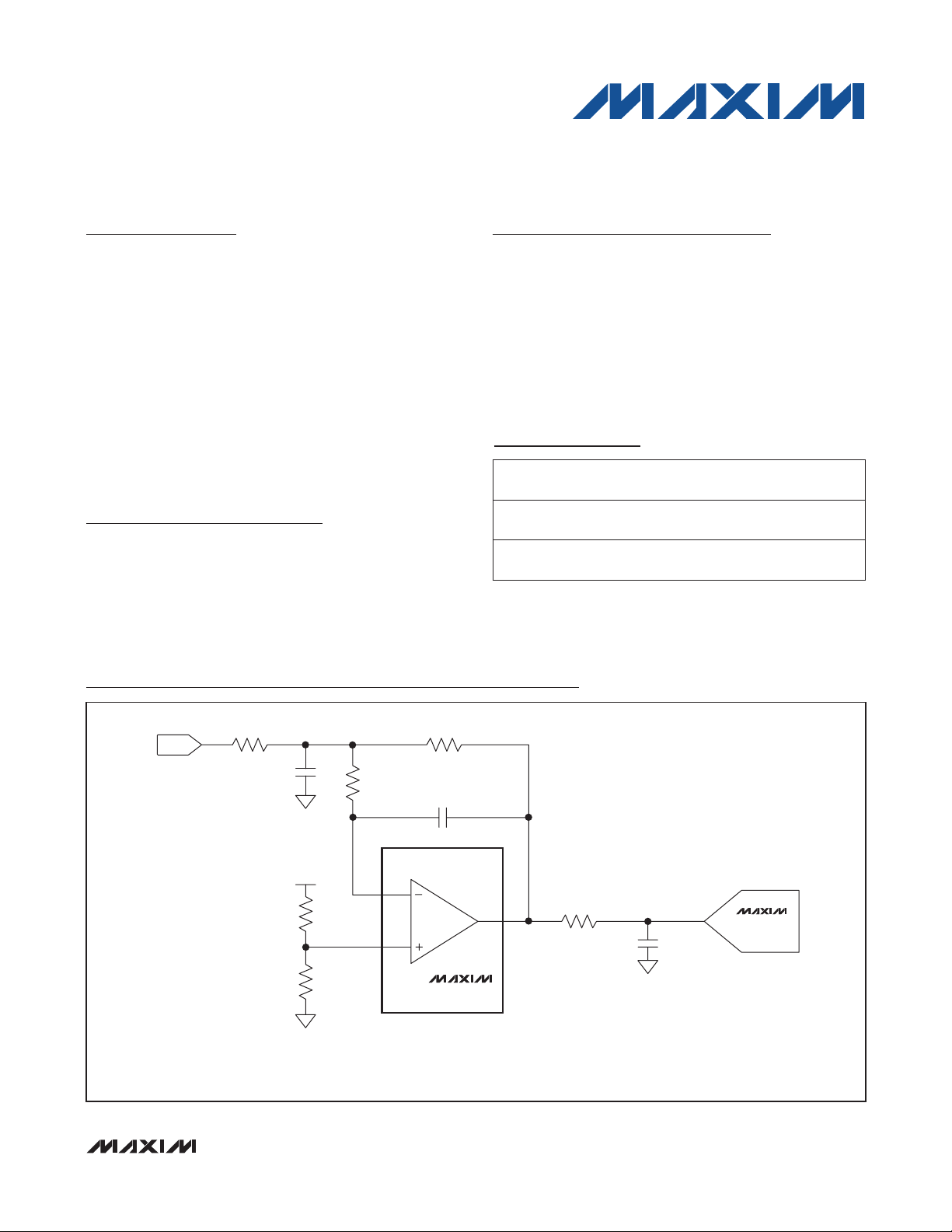
Typical Application Circuit
INPUT
USING THE MAX9614 OUTPUT AMPLIFIER AS AN ANTI-ALIASING FILTER (CORNER FREQUENCY = 1.3kHz) TO MAXIMIZE NYQUIST BANDWIDTH.
66.5kI
4.7nF
20kI
20kI
121kI
V
CC
VCC/2
66.5kI
220pF
MAX9614
1.21kI
100nF
MAX11613
ADC
_______________________________________________________________ Maxim Integrated Products 1
For pricing, delivery, and ordering information, please contact Maxim Direct at 1-888-629-4642,
or visit Maxim’s website at www.maxim-ic.com.
Page 2
Low-Power Single/Dual, Rail-to-Rail Op Amps
ABSOLUTE MAXIMUM RATINGS
IN+, IN-, SHDN, VCC to GND.................................. -0.3V to +6V
OUT to GND ................................................-0.3V to V
CC
+ 0.3V
Short-Circuit (GND) Duration, OUT, OUTA, OUTB ................. 5s
Continuous Input Current (any pin) ................................. Q20mA
Thermal Limits (Note 1) Multilayer PCB
Continuous Power Dissipation (T
= +70NC)
A
6-Pin SC70 (derate 3.1mW/NC above +70NC) .............245mW
B
.......................................................................326.5NC/W
JA
B
.......................................................................... 115NC/W
JC
Note 1: Package thermal resistances were obtained using the method described in JEDEC specification JESD51-7, using a 4-layer
board. For detailed information on package thermal considerations, refer to www.maxim-ic.com/thermal-tutorial.
Stresses beyond those listed under “Absolute Maximum Ratings” may cause permanent damage to the device. These are stress ratings only, and functional
operation of the device at these or any other conditions beyond those indicated in the operational sections of the specifications is not implied. Exposure to absolute
maximum rating conditions for extended periods may affect device reliability.
ELECTRICAL CHARACTERISTICS
(VCC = V
MAX9614/MAX9616
SHDN
= 3.3V, V
unless otherwise noted.) (Note 2)
PARAMETER SYMBOL CONDITIONS MIN TYP MAX UNITS
DC CHARACTERISTICS
Input Voltage Range V
Input Offset Voltage V
Input Offset Voltage Drift V
Input Bias Current (Note 3) I
Input Offset Current (Note 3) I
Common-Mode Rejection Ratio CMRR
Open-Loop Gain A
Output Short-Circuit Current
(Note 4)
Output Voltage Low V
IN+
= V
= VCM = GND, RL = 10kI to VCC/2, TA = -40NC to +125NC. Typical values are at TA = +25NC,
IN-
, V
IN+
Guaranteed by CMRR test -0.1
IN-
TA = +25NC
T
= -40NC to +125NC, after power-up
OS
- TC 1 7.5
OS
A
autocalibration
T
= -40NC to +125NC
A
TA = -40NC to +25°C
= +70NC
T
B
A
T
= +85NC
A
T
= +125NC
A
TA = -40NC to +25°C
T
= +70NC
OS
A
T
= +85NC
A
T
= +125NC
A
V
= -0.1V to VCC - 1.4V, TA = +25NC
CM
V
= -0.1V to VCC - 1.4V, TA = -40NC to
CM
+125NC
+0.4V P V
OL
+0.4V P V
To V
I
SC
CC
To GND 75
P VCC - 0.4V, RL = 10kI
OUT
P VCC - 0.4V, RL = 600I
OUT
RL = 10kI
= 600I
R
OL
L
R
L
= 32I
8-Pin SC70 (derate 3.1mW/NC above +70NC) .............245mW
B
JA ..........................................................................
B
.......................................................................... 115NC/W
JC
Operating Temperature Range ........................ -40NC to +125NC
Junction Temperature .....................................................+150NC
Lead Temperature (soldering, 10s) ................................+300NC
Soldering Temperature (reflow) ......................................+240NC
V
CC
- 1.4
17 100
165
750
1 1.55
45
135
1.55 nA
0.5
7
25
4000
80 95
78
99 115
93 110
275
1 11
11 100
170
326NC/W
V
FV
FV/NC
pA
pA
dB
dB
mA
mV
2 ______________________________________________________________________________________
Page 3

Low-Power Single/Dual, Rail-to-Rail Op Amps
ELECTRICAL CHARACTERISTICS (continued)
(VCC = V
unless otherwise noted.) (Note 2)
Output Voltage High V
AC CHARACTERISTICS
Input Voltage Noise Density e
Input Voltage Noise Total noise
Input Current Noise Density I
Gain Bandwidth GBW 2.8 MHz
Slew Rate SR 1.3
Capacitive Loading C
Total Harmonic Distortion THD f = 10kHz, V
POWER-SUPPLY CHARACTERISTICS
Power-Supply Range V
Power-Supply Rejection Ratio PSRR
Quiescent Current I
Shutdown Supply Current
Shutdown Input Low V
Shutdown Input High V
Output Impedance in Shutdown
Turn-On Time from SHDN
Power-Up Time t
= 3.3V, V
SHDN
PARAMETER SYMBOL CONDITIONS MIN TYP MAX UNITS
Note 2: All devices are 100% production tested at TA = +25NC. Temperature limits are guaranteed by design.
Note 3: Guaranteed by design, not production tested.
Note 4: Do not exceeed package thermal dissipation in the Absolute Maximum Ratings section.
IN+
= V
= VCM = GND, RL = 10kI to VCC/2, TA = -40NC to +125NC. Typical values are at TA = +25NC,
IN-
V
-11VCC -
CC
V
-
CC
100
85 106
83
2
VCC -
30
V
-
CC
560
5
170 255
350
10 ms
OH
n
n
LOAD
CC
CC
I
SHDN
IL
IH
R
OUT_SHDN
t
ON
UP
RL = 10kI
= 600I
R
L
= 32I
R
L
f = 10kHz 28
0.1Hz P f P 10Hz
f = 10kHz 0.1
No sustained oscillation 200 pF
= 2V
OUT
Guaranteed by PSRR 2.5 5.5 V
T
= +25NC
A
T
= -40NC to +125NC
A
TA = +25NC, per amplifier
T
= -40NC to +125NC, per amplifier
A
MAX9614 only 1
MAX9614 only 0.5 V
MAX9614 only 1.4 V
MAX9614 only 10
MAX9614 only 20
, AV = 1V/V -85 dB
P-P
mV
nV/√Hz
FV
fA/√Hz
V/Fs
dB
FA
FA
MI
Fs
MAX9614/MAX9616
P-P
_______________________________________________________________________________________ 3
Page 4
Low-Power Single/Dual, Rail-to-Rail Op Amps
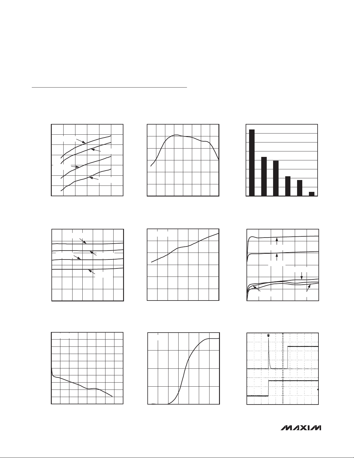
SUPPLY CURRENT (µA)
MAX9614 toc01
Typical Operating Characteristics
(VCC = 3.3V, V
IN+
= V
= 0V, VCM = VCC/2, RL = 10kI to VCC/2, values are at TA = +25NC, unless otherwise noted.)
IN-
MAX9614/MAX9616
OFFSET VOLTAGE
vs. COMMON-MODE VOLTAGE
250
200
TA = +125°C
150
100
50
TA = +25°C
OFFSET VOLTAGE (µV)
0
-50
-100
-0.5 2.5
COMMON-MODE VOLTAGE (V)
TA = -40°C
TA = +85°C
2.01.51.00.50
OFFSET VOLTAGE vs. SUPPLY VOLTAGE
60
50
40
30
20
OFFSET VOLTAGE (µV)
10
0
1.5 5.5
SUPPLY VOLTAGE (V)
MAX9614 toc02
OCCURANCE (%)
5.04.54.03.53.02.52.0
OFFSET VOLTAGE HISTOGRAM
40
35
30
25
20
15
10
5
0
0 60
OFFSET VOLTAGE (µV)
INPUT BIAS CURRENT
SUPPLY CURRENT vs. SUPPLY VOLTAGE
300
TA = +125°C
250
200
TA = +25°C
150
100
SUPPLY CURRENT (µA)
50
0
2.5 6.0
SUPPLY VOLTAGE (V)
TA = +85°C
TA = -40°C
INPUT BIAS CURRENT vs.
COMMON-MODE VOLTAGE
1.0
TA = +25°C
0.8
0.6
0.4
0.2
0
-0.2
-0.4
INPUT BIAS CURRENT (pA)
-0.6
-0.8
-1.0
0 4.0
COMMON-MODE VOLTAGE (V)
MAX9614 toc04
5.55.04.54.03.53.0
MAX9614 toc07
3.53.02.0 2.51.0 1.50.5
SUPPLY CURRENT vs. TEMPERATURE
300
R
= NO LOAD
LOAD
250
200
150
100
50
0
TEMPERATURE (°C)
7550250-25-50 125
INPUT BIAS CURRENT
vs. TEMPERATURE
100
VCM = 0V
10
1
INPUT BIAS CURRENT (pA)
0.1
0.01
-50 125
TEMPERATURE (°C)
100
1007550250-25
10,000
1000
MAX9614 toc05
100
10
1
INPUT BIAS CURRENT (pA)
0.1
0.01
MAX9614 toc08
V
OUT
200mV/div
GND
V
CC
2V/div
GND
vs. COMMON-MODE VOLTAGE
TA = +125°C
TA = +85°C
TA = -40°C
0 3.0
COMMON-MODE VOLTAGE (V)
POWER-UP TRANSIENT
4 ______________________________________________________________________________________
MAX9614 toc03
504010 20 30
MAX9614 toc06
TA = +25°C
TA = 0°C
2.52.01.51.00.5
MMAX9614-16 toc09
4ms/div
Page 5

Low-Power Single/Dual, Rail-to-Rail Op Amps
FREQUENCY (Hz)
FREQUENCY (Hz)
Typical Operating Characteristics (continued)
(VCC = 3.3V, V
IN+
= V
= 0V, VCM = VCC/2, RL = 10kI to VCC/2, values are at TA = +25NC, unless otherwise noted.)
IN-
MAX9614/MAX9616
COMMON-MODE REJECTION RATIO
vs. FREQUENCY
100
90
80
70
60
50
40
30
20
COMMON-MODE REJECTION RATIO (dB)
10
0
0.01 10,000
FREQUENCY (kHz)
INPUT CURRENT NOISE vs. FREQUENCY
0.30
0.25
0.20
0.15
0.10
INPUT CURRENT NOISE (fA/√Hz)
0.05
0
10 100k
FREQUENCY (Hz)
10k1k100
POWER-SUPPLY REJECTION RATIO
120
vs. FREQUENCY
100
MAX9614 toc10
80
60
40
20
POWER-SUPPLY REJECTION RATIO (dB)
MAX9614-16 toc13
200mV/div
2V/div
0
0.001 10,000
FREQUENCY (kHz)
V
GND
GND
OUT
V
RECOVERY FROM SHUTDOWN
CC
10µs/div
MAX9614-16 toc14
10001001010.1
MAX9614-16 toc11
10001001010.10.01
INPUT VOLTAGE NOISE vs. FREQUENCY
100
90
80
70
60
50
40
30
INPUT VOLTAGE NOISE (nV/√Hz)
20
10
0
100 100k
10k1k
TOTAL HARMONIC DISTORTION
-60
V
= 2V
IN
P-P
AV = 1V/V
-70
-80
-90
-100
TOTAL HARMONIC DISTORTION (dB)
-110
-120
10 100k
FREQUENCY (Hz)
MAX9614 toc12
MAX9614 toc15
10k1k100
TOTAL HARMONIC DISTORTION
PLUS NOISE
0
VIN = 2V
P-P
AV = 1V/V
-20
-40
-60
-80
-100
TOTAL HARMONIC DISTORTION PLUS NOISE (dB)
-120
10 100k
10k1k100
_______________________________________________________________________________________ 5
3.4
3.3
3.2
MAX9614-16 toc16
3.1
3.0
2.9
2.8
2.7
OUTPUT HIGH VOLTAGE (V)
2.6
2.5
2.4
0 30
OUTPUT HIGH VOLTAGE
vs. OUTPUT SOURCE CURRENT
TA = -40°C
TA = +25°C
TA = +85°C
TA = +125°C
252015105
OUTPUT SOURCE CURRENT (mA)
0.18
0.16
0.14
MAX9614-16 toc17
0.12
0.10
0.08
0.06
OUTPUT LOW VOLTAGE (V)
0.04
0.02
0
0 30
OUTPUT LOW VOLTAGE
vs. OUTPUT SINK CURRENT
TA = +85°C
MAX9614-16 toc18
TA = +125°C
TA = +25°C
TA = -40°C
252015105
OUTPUT SINK CURRENT (mA)
Page 6

Low-Power Single/Dual, Rail-to-Rail Op Amps
10,000
1000
Typical Operating Characteristics (continued)
(VCC = 3.3V, V
IN+
= V
= 0V, VCM = VCC/2, RL = 10kI to VCC/2, values are at TA = +25NC, unless otherwise noted.)
IN-
V
OUT
1µV/div
0.1Hz TO 10Hz NOISE
MAX9614 toc19
OPEN-LOOP GAIN (dB)
MAX9614/MAX9616
STABILITY vs. CAPACITIVE WITH
SERIES ISOLATION RESISTOR
80
70
60
50
40
30
RESISTIVE LOAD (I)
20
10
0
0 1200
STABLE
UNSTABLE
CAPACITIVE LOAD (pF)
OPEN-LOOP GAIN vs. FREQUENCY
120
100
80
60
40
20
0
0.001
FREQUENCY (kHz)
MAX9614-16 toc22
1000800200 400 600
V
OUT
50mV/div
GND
V
50mV/div
GND
STABILITY vs. CAPACITIVE AND
RESISTIVE LOAD IN PARALLEL
14
12
MAX9614-16 toc20
10
8
6
RESISTIVE LOAD (kI)
4
2
STABLE
10001001010.10.01
0
0
UNSTABLE
CAPACITIVE LOAD (pF)
MAX9614 toc21
900800700600500400300200100
100mV STEP RESPONSE
= 200pF
C
LOAD
IN
1µs/div
MAX9614-16 toc23
RECOVERY FROM SATURATION
OUTPUT SATURATED TO GND
AV = 10V/V
OUT
V
IN
MAX9614-16 toc25
10µs/div
V
OUT
1V/div
GND
1V/div
GND
2V STEP RESPONSE
= 200pF
C
LOAD
V
IN
4µs/div
MAX9614-16 toc24
V
500mV/div
GND
50mV/div
GND
6 ______________________________________________________________________________________
Page 7

Low-Power Single/Dual, Rail-to-Rail Op Amps
Typical Operating Characteristics (continued)
(VCC = 3.3V, V
IN+
= V
= 0V, VCM = VCC/2, RL = 10kI to VCC/2, values are at TA = +25NC, unless otherwise noted.)
IN-
MAX9614/MAX9616
RECOVERY FROM SATURATION
V
OUT
1V/div
GND
1V/div
GND
OUTPUT SATURATED TO V
AV = 10V/V
V
IN
10µs/div
CC
MAX9614-16 toc26
OUTPUT IMPEDANCE vs. FREQUENCY
25
20
15
10
RESISTANCE (I)
5
0
0 10,000
FREQUENCY (kHz)
MAX9614-16 toc27
V
IN
1V/div
V
OUT
1V/div
10001001010.1
NO PHASE REVERSAL
200µs/div
MAX9614 toc28
Pin Configuration
TOP VIEW
NOT TO SCALE
IN+
GND
+
1
2
IN-
3
MAX9614
6
V
CC
5
SHDN
4
OUT
OUTA
INA-
INA+
GND
+
1
2
3
4
MAX9616
V
8
CC
OUTB
7
INB-
6
INB+
5
6 SC70
8 SC70
Pin Description
PIN
MAX9614 MAX9616
1 — IN+ Positive Input
— 3 INA+ Positive Input A
— 5 INB+ Positive Input B
2 4 GND Ground
3 — IN- Negative Input
— 2 INA- Negative Input A
— 6 INB- Negative Input B
4 — OUT Output
— 1 OUTA Output A
— 7 OUTB Output B
5 —
6 8 V
_______________________________________________________________________________________ 7
NAME FUNCTION
SHDN
CC
Active-Low Shutdown
Positive Power Supply. Bypass with a 0.1FF capacitor to ground.
Page 8
Low-Power Single/Dual, Rail-to-Rail Op Amps
Detailed Description
The MAX9614/MAX9616 are low-power op amps ideal
for signal processing applications due to the devices’
high precision and CMOS inputs.
The MAX9614 also features a low-power shutdown mode
that greatly reduces quiescent current while the device
is not operational.
The MAX9614/MAX9616 self-calibrate on power-up to eliminate effects of temperature and power-supply variation.
RF Immunity
The MAX9614/MAX9616 feature robust internal EMI filters
that reduce the devices’ susceptibility to high-frequency
RF signals such as from wireless and mobile devices.
This, combined with excellent DC and AC specifications,
makes these devices ideal for a wide variety of portable
audio and sensitive signal-conditioning applications.
MAX9614/MAX9616
Applications Information
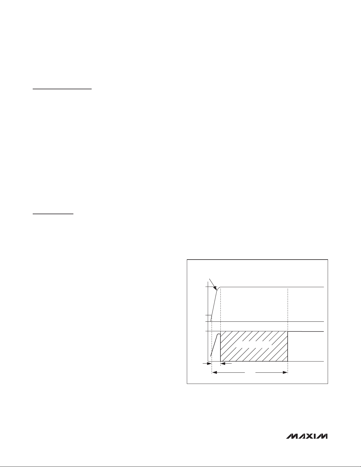
Power-Up Autotrim
The MAX9614/MAX9616 feature an automatic power-up
autotrim that self-calibrates the V
to less than 100FV of input offset voltage. The autotrim
sequence takes approximately 10ms to complete, and is
triggered by an internal power-on reset (POR) circuitry.
During this time, the inputs and outputs are put into high
impedance and left unconnected. This self-calibration
feature allows the device to eliminate input offset voltage
effects due to power supply and operating temperature
variation simply by cycling its power.
Take care to ensure that the power supply settles within
0.4ms of power-up after it crosses a POR threshold of
0.5V to ensure that a stable power supply is present
when it steps through its autotrim sequence. If the power
supply glitches below the 0.5V threshold, the POR circuitry reactivates during next power-up.
Shutdown Operation
The MAX9614 features an active-low shutdown mode
that puts both inputs and outputs into a high-impedance
state. In this mode, the quiescent current is less than
1FA. Putting the output in high-impedance allows multiple signal outputs to be multiplexed onto a single output
line without the additional external buffers. The device
of these devices
OS
does not self-calibrate when exiting shutdown mode,
and retains its power-up trim settings. The device also
instantly recovers from shutdown.
The shutdown logic levels of the device are independent
of supply allowing the shutdown to operate by either a
1.8V or 3.3V microcontroller.
Interfacing with the MAX11613
The MAX9616 dual amplifier’s low power and tiny size
is ideal for driving multichannel analog-to-digital converters (ADCs) such as the MAX11613 (see the Typical
Application Circuit). The MAX11613 is a low-power,
2
12-bit I
or two differential channels in an 8-pin FMAX
C ADC that measures either four single-ended
®
package. Operating from a single 3V or 3.3V supply, the
MAX11613 draws a low 380FA supply current when sampling at 10ksps.The MAX11613 family also offers pincompatible 5V ADCs (MAX11612) and 8-bit (MAX11601)
and 10-bit (MAX11607) options.
The MAX9614/MAX9616’s output voltage low is
designed to be especially close to ground—it is only
11mV above ground, allowing maximum dynamic
range in single-supply applications. High output current and capacitance drive capability of the part help
it to be useful in ADC driver and line-driver.
TIME FOR POWER SUPPLY
TO SETTLE
5V
V
CC
0.5V
0V
2V
V
OUT*
0V
0.4
ms
Figure 1. Autotrim Timing Diagram
AMPLIFIER AUTOTRIM
10ms
CALIBRATED
AMPLIFIER
ACTIVE
µMAX is a registered trademark of Maxim Integrated Products, Inc.
8 ______________________________________________________________________________________
Page 9

Low-Power Single/Dual, Rail-to-Rail Op Amps
Input Bias Current
The MAX9614/MAX9616 feature a high-impedance
CMOS input stage and a specialized ESD structure
that allows low input bias current operation at low
input common-mode voltages. Low input bias current
is useful when interfacing with high-ohmic sensors. It
is also beneficial for designing transimpedance amplifiers for photodiode sensors. This makes the MAX9614/
MAX9616 ideal for ground referenced medical and
industrial sensor applications.
Active Filters
MAX9614/MAX9616
The MAX9614/MAX9616 are ideal for a wide variety
of active filter circuits that make use of their rail-to-rail
output stages and high impedance CMOS inputs. The
Typical Application Circuit shows an example multiple
feedback active filter circuit with a corner frequency
of 1.3kHz. At low frequencies, the amplifier behaves
like a simple low-distortion inverting amplifier of gain =
-1, while its high bandwidth gives excellent stopband
attenuation above its corner frequency. See the Typical
Application Circuit.
Chip Information
PROCESS: BiCMOS
_______________________________________________________________________________________ 9
Page 10
Low-Power Single/Dual, Rail-to-Rail Op Amps
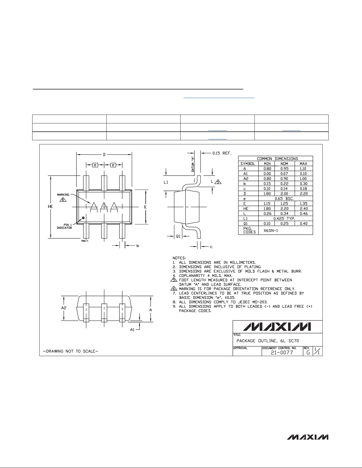
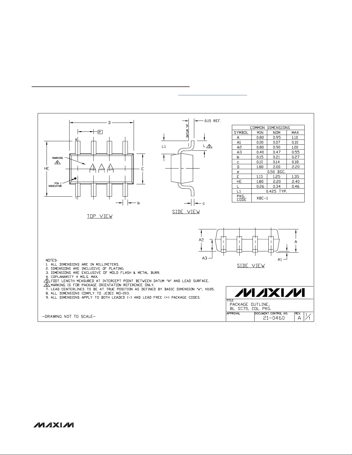
SC70, 6L.EPS
Package Information
For the latest package outline information and land patterns, go to www.maxim-ic.com/packages. Note that a “+”, “#”, or “-” in the
package code indicates RoHS status only. Package drawings may show a different suffix character, but the drawing pertains to the
package regardless of RoHS status.
PACKAGE TYPE PACKAGE CODE OUTLINE NO. LAND PATTERN NO.
6 SC70 X6SN-1
8 SC70 X8SN-1
21-0077 90-0189
21-0460 —
MAX9614/MAX9616
10 _____________________________________________________________________________________
Page 11
Low-Power Single/Dual, Rail-to-Rail Op Amps
Package Information (continued)
For the latest package outline information and land patterns, go to www.maxim-ic.com/packages. Note that a “+”, “#”, or “-” in the
package code indicates RoHS status only. Package drawings may show a different suffix character, but the drawing pertains to the
package regardless of RoHS status.
MAX9614/MAX9616
______________________________________________________________________________________ 11
Page 12
Low-Power Single/Dual, Rail-to-Rail Op Amps
Revision History
REVISION
NUMBER
0 8/10 Initial release —
REVISION
DATE
MAX9614/MAX9616
DESCRIPTION
PAGES
CHANGED
Maxim cannot assume responsibility for use of any circuitry other than circuitry entirely embodied in a Maxim product. No circuit patent licenses are implied.
Maxim reserves the right to change the circuitry and specifications without notice at any time.
12 Maxim Integrated Products, 120 San Gabriel Drive, Sunnyvale, CA 94086 408-737-7600
©
2010 Maxim Integrated Products Maxim is a registered trademark of Maxim Integrated Products, Inc.
 Loading...