

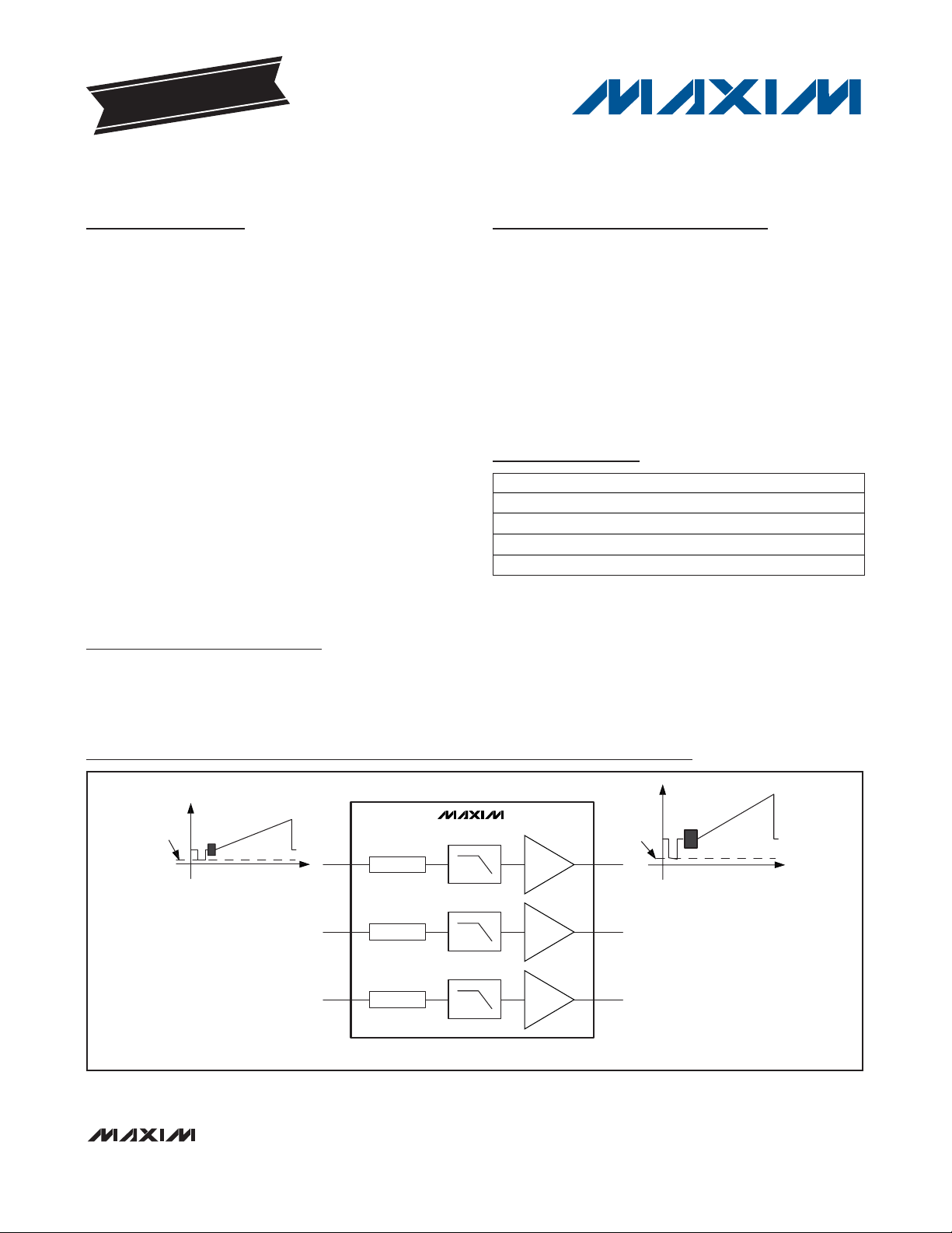
General Description
The MAX9586–MAX9589 are small, low-power, multichannel video amplifiers with integrated reconstruction
filters and input clamps. Specially suited for standarddefinition video signals, these devices are ideal for a
wide range of television and set-top box applications.
The video signals from the outputs of a digital-to-analog
converter (DAC) are AC-coupled to the inputs of the
MAX9586–MAX9589. External video signals, in which
the DC bias is usually not known, can also be AC-coupled to the inputs of the MAX9586–MAX9589. The input
sync-tip clamps set the DC level of composite video or
luma signals, and the input bias circuits set the DC
level of chroma signals.
The reconstruction filter typically has ±1dB passband
flatness at 8.5MHz and 55dB attenuation at 27MHz. The
amplifiers have 2V/V gain and the outputs can be DCcoupled to a 75Ω load, which is the equivalent of two
video loads, or AC-coupled to a 150Ω load.
The MAX9586–MAX9589 operate from a 2.7V to 3.6V single supply and are specified over the -40°C to +125°C
automotive temperature range. The MAX9586–MAX9589
are offered in small SOT23 and µMAX®packages.
Applications
Set-Top Boxes
Televisions
Features
o Single- (MAX9586), Dual- (MAX9587),
Triple- (MAX9588), and Quad- (MAX9589)
Channel Devices
o 8.5MHz, ±1dB Passband
o 55dB Attenuation at 27MHz
o Fixed Gain of 2V/V
o Low Power: 4.25mA per Channel
o 2.7V to 3.6V Single-Supply Operation
o Small SOT23 and µMAX Packages
MAX9586–MAX9589
Single, Dual, Triple, and Quad Standard-Definition
Video Filter Amplifiers with AC-Coupled Input Buffers
________________________________________________________________
Maxim Integrated Products
1
Block Diagrams
19-0744; Rev 6; 2/11
For pricing, delivery, and ordering information, please contact Maxim Direct at 1-888-629-4642,
or visit Maxim’s website at www.maxim-ic.com.
EVALUATION KIT
AVAILABLE
µMAX is a registered trademark of Maxim Integrated Products, Inc.
Ordering Information
Note: All devices are specified over the -40°C to +125°C operating temperature range.
+
Denotes a lead(Pb)-free/RoHS-compliant package.
T = Tape and reel.
Block Diagrams continued at end of data sheet.
Pin Configurations and Selector Guide located at end of
data sheet.
PART PIN-PACKAGE CHANNELS
MAX9586AZK+T
MAX9587AZT+T
MAX9588AUA+T
MAX9589AUB+T
5 Thin SOT23
6 Thin SOT23
8 µMAX
10 µMAX
1
2
3
4
UNKNOWN
BIAS
INA
INB
INC
CLAMP
CLAMP
BIAS
MAX9588
LPF
LPF
LPF
AV = 2V/V
AV = 2V/V
AV = 2V/V
OUTA
OUTB
OUTC
300mV
MAX9586–MAX9589
Single, Dual, Triple, and Quad Standard-Definition
Video Filter Amplifiers with AC-Coupled Input Buffers
2 _______________________________________________________________________________________
ABSOLUTE MAXIMUM RATINGS
ELECTRICAL CHARACTERISTICS
(V
DD
= 3.3V, V
GND
= 0V, VRL= no load, TA= T
MIN
to T
MAX
, unless otherwise noted. Typical values are at TA= +25°C.) (Note 1)
Stresses beyond those listed under “Absolute Maximum Ratings” may cause permanent damage to the device. These are stress ratings only, and functional
operation of the device at these or any other conditions beyond those indicated in the operational sections of the specifications is not implied. Exposure to
absolute maximum rating conditions for extended periods may affect device reliability.
VDDto GND..............................................................-0.3V to +4V
IN_ to GND ...............................................................-0.3V to +4V
SHDN to GND...........................................................-0.3V to +4V
OUT_ Short Circuit Duration to V
DD
, GND .................Continuous
Continuous Input Current
IN_, SHDN ....................................................................±20mA
Continuous Power Dissipation (T
A
= +70°C)
5-Pin Thin SOT23 (derate 9.1mW/°C above +70°C)....727mW
6-Pin Thin SOT23 (derate 9.1mW/°C above +70°C)....727mW
8-Pin µMAX (derate 4.5mW/°C above +70°C) .............362mW
10-Pin µMAX (derate 5.6mW/°C above +70°C) ...........444mW
Operating Temperature Range .........................-40°C to +125°C
Junction Temperature......................................................+150°C
Storage Temperature Range .............................-65°C to +150°C
Lead Temperature (soldering, 10s) .................................+300°C
Soldering Temperature (reflow) .......................................+260°C
PARAMETER SYMBOL CONDITIONS MIN TYP MAX UNITS
Supply Voltage Range V
Supply Current I
Sync-Tip Clamp Level V
Input Voltage Range V
Sync Crush
Input Clamping Current Sync-tip clamp 1 2 µA
Maximum Input Source
Resistance
Bias Voltage V
Input Resistance Bias circuit 11 kΩ
DC Voltage Gain (Note 2) A
DC Gain Matching Guaranteed by DC voltage gain -2 0 +2 %
Output Level
DD
DD
CLP
IN
BIAS
V
Guaranteed by PSRR 2.7 3.6 V
Per channel 4.25 8 mA
Sync-tip clamp 0.24 0.41 V
Guaranteed by DC
voltage gain
Sync-tip clamp, percentage reduction in sync pulse
(0.3V
measurement, measured at input
Bias circuit 0.40 0.50 0.62 V
RL = 150Ω to GND
Measured at V
IN_ = 0.1µF to GND,
R
), guaranteed by input clamping current
P-P
= 150Ω to GND
L
VDD = 2.7V, sync-tip clamp
input
VDD = 2.7V, bias input 1.05
VDD = 3V, sync-tip clamp input 1.2
V
DD
,
OUT
1.05
= 3V, bias input 1.2
2%
300 Ω
VDD = 2.7V, VIN = V
+ 1.05V)
(V
CLP
VDD = 3V, VIN = V
+ 1.2V)
(V
CLP
VDD = 2.7V, VIN = V
±0.525V
V
= 3V, VIN = V
DD
±0.600V
Sync-tip clamp 0.2 0.3 0.4
Bias circuit 1.3
CLP
CLP
BIAS
BIAS
to
to
1.95 2.00 2.04
1.95 2.00 2.04
1.95 2.00 2.04
1.95 2.00 2.04
V
V/V
P-P
V
MAX9586–MAX9589
Single, Dual, Triple, and Quad Standard-Definition
Video Filter Amplifiers with AC-Coupled Input Buffers
_______________________________________________________________________________________ 3
ELECTRICAL CHARACTERISTICS (continued)
(V
DD
= 3.3V, V
GND
= 0V, VRL= no load, TA= T
MIN
to T
MAX
, unless otherwise noted. Typical values are at TA= +25°C.) (Note 1)
PARAMETER SYMBOL CONDITIONS MIN TYP MAX UNITS
Output-Voltage Swing
Sync-tip clamp
Measured at output, V
V
= V
IN
R
L
to (V
CLP
CLP
= 150Ω to -0.2V
Measured at output, V
= V
V
IN
R
L
to (V
CLP
CLP
= 150Ω to VDD/2
Measured at output, V
V
= V
IN
R
L
to (V
CLP
CLP
= 150Ω to -0.2V
Measured at output, V
= V
V
IN
R
L
to (V
CLP
CLP
= 150Ω to VDD/2
Measured at output, V
3.135V, V
1.05V), R
= V
IN
CLP
= 75Ω to -0.2V
L
Measured at output, V
V
= V
IN
= 150Ω to -0.2V
R
L
BIAS
±0.525V,
Measured at output, V
= V
V
IN
R
= 150Ω to VDD/2
L
BIAS
±0.500V,
= 2.7V,
DD
+ 1.05V),
= 2.7V,
DD
+ 1.05V),
= 3V,
DD
+ 1.2V),
= 3V,
DD
+ 1.2V),
=
DD
to (V
CLP
= 2.7V,
DD
= 2.7V,
DD
2.1
2.1
2.4
2.4
+
2.1
2.1
2.0
V
P-P
Output Short-Circuit
Current
Output Resistance R
OUT
Bias Circuit
Measured at output, V
V
= V
IN
= 150Ω to -0.2V
R
L
BIAS
±0.600V,
Measured at output, V
= V
V
IN
R
= 150Ω to VDD/2
L
BIAS
±0.500V,
Measured at output, V
3.135V, V
= 75Ω to -0.2V
R
L
IN
= V
BIAS
= 3V,
DD
= 3V,
DD
=
DD
±0.525V,
2.4
2.0
2.1
Short to GND (sourcing) 140
Short to V
V
OUT
(sinking) 70
DD
= 1.5V, -10mA ≤ I
≤ +10mA 0.2 Ω
LOAD
mA
MAX9586–MAX9589
Single, Dual, Triple, and Quad Standard-Definition
Video Filter Amplifiers with AC-Coupled Input Buffers
4 _______________________________________________________________________________________
ELECTRICAL CHARACTERISTICS (continued)
(V
DD
= 3.3V, V
GND
= 0V, VRL= no load, TA= T
MIN
to T
MAX
, unless otherwise noted. Typical values are at TA= +25°C.) (Note 1)
Note 1: All devices are 100% production tested at TA= +25°C. Specifications over temperature limits are guaranteed by design.
Note 2: Voltage gain (A
V
) is a two-point measurement in which the output-voltage swing is divided by the input-voltage swing.
PARAMETER SYMBOL CONDITIONS MIN TYP MAX UNITS
Power-Supply Rejection
Ratio
Standard-Definition
Reconstruction Filter
Differential Gain DG
Differential Phase DP
2T Pulse-to-Bar K Rating
2T Pulse Response 2T = 200ns 0.2 K%
2T Bar Response
Nonlinearity 5-step staircase 0 %
Group Delay Distortion 100kHz ≤ f ≤ 5.5MHz, outputs are 2V
P eak S i g nal to RM S N oi se 100kHz ≤ f ≤ 5.5MHz 71 dB
Output Impedance f = 5.5MHz 4.8 Ω
All-Hostile Crosstalk f = 4.43MHz -64 dB
2.7V ≤ VDD ≤ 3.6V 48
f = 1MHz, 100mV
±1dB passband flatness 8.5 MHz
= 2V
V
OUT_
reference frequency is
100kHz
5-step modulated staircase of 129mV step size and
286mV peak-to-peak subcarrier amplitude,
f = 4.43MHz
5-step modulated staircase of 129mV step size and
286mV peak-to-peak subcarrier amplitude,
f = 4.43MHz
2T = 200ns, bar time is 18µs; the beginning 2.5%
and the ending 2.5% of the bar time are ignored
2T = 200ns, bar time is 18µs; the beginning 2.5%
and the ending 2.5% of the bar time are ignored
29
0.1 %
0.4 D eg r ees
0.6 K%
0.2 K%
9ns
P-P
P-P
,
f = 5.5MHz -0.15
f = 9.5MHz -3
f = 27MHz -55
P-P
dB
dB
MAX9586–MAX9589
Single, Dual, Triple, and Quad Standard-Definition
Video Filter Amplifiers with AC-Coupled Input Buffers
_______________________________________________________________________________________
5
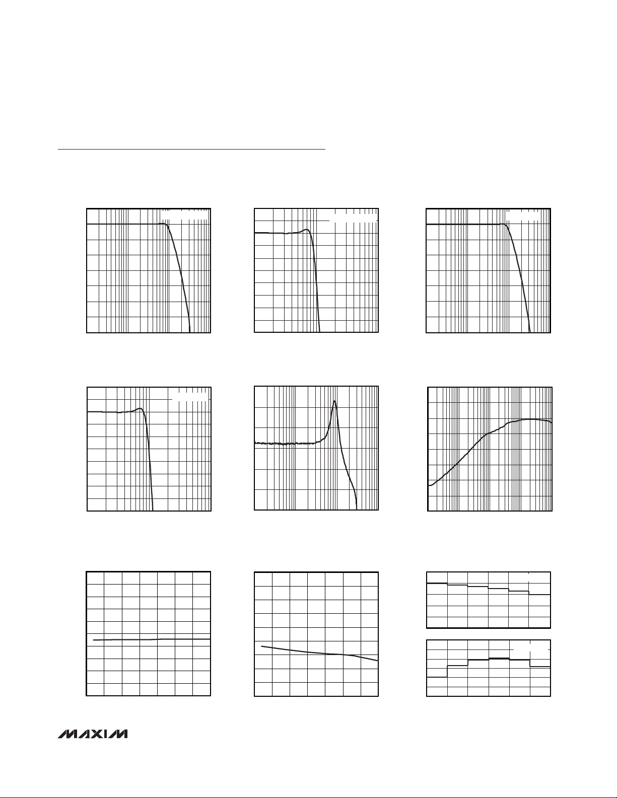
Typical Operating Characteristics
(VDD= V
SHDN
= +3.3V, video outputs have RL = 150Ω connected to GND, TA= +25°C, unless otherwise noted.)
QUIESCENT SUPPLY CURRENT
vs. TEMPERATURE
MAX9586 toc07
TEMPERATURE (°C)
QUIESCENT SUPPLY CURRENT (mA)
1007525 500-25
2.5
3.0
3.5
4.0
4.5
5.0
5.5
6.0
6.5
7.0
2.0
-50 125
VOLTAGE GAIN
vs. TEMPERATURE
MAX9586 toc08
TEMPERATURE (°C)
VOLTAGE GAIN (V/V)
1007525 500-25
1.96
1.97
1.98
1.99
2.00
2.01
2.02
2.03
2.04
1.95
-50 125
SMALL-SIGNAL GAIN
vs. FREQUENCY
MAX9586 toc01
FREQUENCY (Hz)
GAIN (dB)
10M1M
-60
-50
-40
-30
-20
-10
0
10
-70
100k 100M
V
OUT
= 100mV
P-P
SMALL-SIGNAL GAIN FLATNESS
vs. FREQUENCY
MAX9856 toc02
FREQUENCY (Hz)
GAIN (dB)
10M
-7
-6
-5
-4
-3
-2
-1
0
1
2
-8
1M 100M
V
OUT
= 100mV
P-P
LARGE-SIGNAL GAIN
vs. FREQUENCY
MAX9586 toc03
FREQUENCY (Hz)
GAIN (dB)
10M1M
-60
-50
-40
-30
-20
-10
0
10
-70
100k 100M
V
OUT
= 2V
P-P
LARGE-SIGNAL GAIN FLATNESS
vs. FREQUENCY
MAX9856 toc04
FREQUENCY (Hz)
GAIN (dB)
10M
-7
-6
-5
-4
-3
-2
-1
0
1
2
-8
1M 100M
V
OUT
= 2V
P-P
GROUP DELAY
vs. FREQUENCY
MAX9586 toc05
FREQUENCY (Hz)
DELAY (ns)
10M1M
20
40
60
80
100
120
0
100k 100M
POWER-SUPPLY REJECTION RATIO
vs. FREQUENCY
MAX9586 toc06
FREQUENCY (Hz)
PSRR (dB)
10M1M
-60
-70
-50
-40
-30
-20
-10
0
-80
10k 100k 100M
DIFFERENTIAL GAIN AND PHASE
MAX9586 toc09
DIFFERENTIAL GAIN (%)
65432
-0.3
-0.2
-0.1
0
0.1
-0.4
DIFFERENTIAL PHASE (deg)
-0.2
0
0.2
0.4
0.6
0.8
-0.4
17
6543217
f = 4.43MHz
f = 4.43MHz
MAX9586–MAX9589
Single, Dual, Triple, and Quad Standard-Definition
Video Filter Amplifiers with AC-Coupled Input Buffers
6 _______________________________________________________________________________________
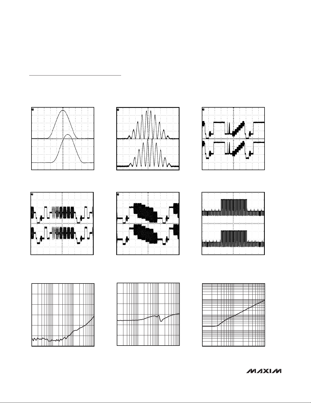
Typical Operating Characteristics (continued)
(VDD= V
SHDN
= +3.3V, video outputs have RL = 150Ω connected to GND, TA= +25°C, unless otherwise noted.)
2T RESPONSE
MAX9586 toc10
100ns/div
OUT_
400mV/div
IN_
200mV/div
12.5T RESPONSE
MAX9586 toc11
400ns/div
OUT_
400mV/div
IN_
200mV/div
NTC-7 VIDEO TEST SIGNAL
MAX9586 toc12
10μs/div
OUT_
1V/div
IN_
500mV/div
PAL MULTIBURST RESPONSE
MAX9586 toc13
10μs/div
OUT_
1V/div
IN_
500mV/div
PAL COLOR BARS
MAX9586 toc14
10μs/div
OUT_
1V/div
IN_
500mV/div
FIELD SQUARE-WAVE RESPONSE
MAX9586 toc15
2ms/div
OUT_
1V/div
IN_
500mV/div
INPUT-TO-INPUT CROSSTALK
vs. FREQUENCY
MAX9586 toc16
FREQUENCY (Hz)
GAIN (dB)
10M1M
-100
-80
-60
-40
-20
0
-120
100k 100M
OUTPUT-TO-OUTPUT CROSSTALK
vs. FREQUENCY
MAX9586 toc17
FREQUENCY (Hz)
GAIN (dB)
10M1M
-100
-80
-60
-40
-20
0
-120
100k 100M
OUTPUT IMPEDANCE
vs. FREQUENCY
MAX9586 toc18
FREQUENCY (Hz)
OUTPUT IMPEDANCE (Ω)
1M
0.1
1
10
100
0.01
100k 10M

MAX9586–MAX9589
Single, Dual, Triple, and Quad Standard-Definition
Video Filter Amplifiers with AC-Coupled Input Buffers
_______________________________________________________________________________________ 7
Pin Description
Figure 1. Typical Application Circuits for the MAX9586/MAX9587 (Anti-Alias Filter)
PIN
MAX9586 MAX9587 MAX9588 MAX9589
5 SOT23 6 SOT23 8 µMAX 10 µMAX
1———SHDN Active-Low Shutdown Input. Connect to GND to shut down.
2 2 4 5 GND Ground
3 — — — IN Video Input
— 3 1 1 INA Video Input A
— 1 2 2 INB Video Input B
— — 3 3 INC Video Input C
— — — 4 IND Video Input D
4 — — — OUT Video Output
— 4 7 9 OUTA Video Output A
— 6 6 8 OUTB Video Output B
— — 5 7 OUTC Video Output C
— — — 6 OUTD Video Output D
55810V
SHDN
+3.3V
VIDEO
SWITCH
0.1μF
IN
CLAMP
NAME FUNCTION
Positive Power Supply. Bypass to GND with a 0.1µF capacitor.
DD
V
MAX9586
LPF
AV = 2V/V
DD
GND
OUTCVBS
75Ω
3.3V
0.1μF
0.1μF
75Ω
VIDEO
DECODER
MAX9587
0.1μF
INA
VIDEO
SWITCH
0.1μF
CLAMP
INB
BIAS
LPF
LPF
AV = 2V/V
AV = 2V/V
V
GND
OUTALUMA
OUTBCHROMA
DD
75Ω
75Ω
75Ω
75Ω
0.1μF
0.1μF
0.1μF
3.3V
VIDEO
DECODER

MAX9586–MAX9589
Single, Dual, Triple, and Quad Standard-Definition
Video Filter Amplifiers with AC-Coupled Input Buffers
8 _______________________________________________________________________________________
Figure 2. Typical Application Circuits for the MAX9588/MAX9589 (Reconstruction Filter)
V
MPEG
DECODER
DD
V
DD
MAX9588
GND
3.3V
0.1μF
0.1μF
DD
0.1μF
DD
0.1μF
DAC
DAC
DAC
CVBS
V
LUMA
V
CHROMA
MPEG
DECODER
DAC
CVBS
V
DD
0.1μF
INA
INB
INC
INA
CLAMP
CLAMP
BIAS
CLAMP
LPF
LPF
LPF
MAX9589
LPF
AV = 2V/V
AV = 2V/V
AV = 2V/V
AV = 2V/V
OUTA
OUTB
OUTC
V
DD
GND
OUTA
75Ω
CVBS
75Ω
Y
75Ω
C
3.3V
0.1μF
75Ω
CVBS1
DAC
DAC
LUMA
CHROMA
0.1μF
INB
V
DD
0.1μF
INC
V
DD
0.1μF
IND
CLAMP
CLAMP
BIAS
LPF
LPF
LPF
AV = 2V/V
AV = 2V/V
AV = 2V/V
OUTB
OUTC
OUTD
75Ω
75Ω
75Ω
CVBS2
Y
C

MAX9586–MAX9589
Single, Dual, Triple, and Quad Standard-Definition
Video Filter Amplifiers with AC-Coupled Input Buffers
_______________________________________________________________________________________ 9
Detailed Description
The MAX9586–MAX9589 filter and amplify the video
DAC output in applications such as set-top boxes and
televisions. These devices consist of input clamps,
input bias circuits, lowpass filters, and gain of 2V/V output amplifiers capable of driving a standard 150Ω
video load to ground.
Inputs
The input stages of the MAX9586–MAX9589 are either
sync-tip clamps or bias circuits. Sync-tip clamps accept
AC-coupled CVBS or luma video signals with sync pulses. The sync-tip voltage is internally set to 300mV. Bias
circuit inputs accept AC-coupled chroma, a subcarrier
modulated with the color information. The bias voltage
of the bias circuits is approximately 500mV.
Video Filter
The filter passband (±1dB) is typically 8.5MHz, which
makes the device suitable for standard-definition video
signals from all sources (e.g., broadcast and DVD).
Broadcast video signals are channel limited: NTSC signals have 4.2MHz bandwidth and PAL signals have
5MHz bandwidth. Video signals from a DVD player,
however, are not channel limited, so the bandwidth of
DVD video signals can approach the Nyquist limit of
6.75MHz. (Recommendation ITU-R BT.601-5 specifies
13.5MHz as the sampling rate for standard-definition
video). Therefore, the maximum bandwidth of the signal
is 6.75MHz. To ease the filtering requirements, most
modern video systems oversample by two times, clocking the video current DAC at 27MHz.
Outputs
The video output amplifiers can both source and sink
load current, allowing output loads to be DC- or ACcoupled. The amplifier output stage needs approximately 300mV of headroom from either supply rail. The
devices have an internal level-shift circuit that positions
the sync tip at approximately 300mV at the output.
If the supply voltage is greater than 3.135V (5% below
a 3.3V supply), each amplifier can drive two DC-coupled video loads to ground. If the supply is less than
3.135V, each amplifier can drive only one DC-coupled
or AC-coupled video load.
Shutdown (MAX9586)
The MAX9586 draws less than 1µA supply current
when SHDN is low. In shutdown mode, the amplifier
output becomes high impedance.
Applications Information
AC-Coupling the Outputs
The outputs can be AC-coupled since the output stage
can source and sink current as shown in Figure 4.
Coupling capacitors should be 220µF or greater to
keep the highpass filter, formed by the 150Ω equivalent
resistance of the video transmission line, to a corner
frequency of 4.8Hz or below. The frame rate of PAL
systems is 25Hz, and the frame rate of NTSC systems
is 30Hz. The corner frequency should be well below the
frame rate.
Power-Supply Bypassing and Ground
The MAX9586–MAX9589 operate from a single-supply
voltage down to 2.7V, allowing for low-power operation.
Bypass V
DD
to GND with a 0.1µF capacitor. Place all
external components as close as possible to the device.
Figure 3. Loopback Circuit Diagram
CVBS IN
37.5Ω
V
37.5Ω
0.1µF
IN
MAX9526
DOUT
LOOPBACK
OUT
IN
MAX9586
0.1µF
75Ω
OUT

MAX9586–MAX9589
Single, Dual, Triple, and Quad Standard-Definition
Video Filter Amplifiers with AC-Coupled Input Buffers
10 ______________________________________________________________________________________
Figure 4. AC-Coupled Outputs
V
MPEG
DECODER
DD
V
DD
MAX9589
GND
0.1μF
3.3V
DAC
DAC
DAC
CVBS
V
LUMA
V
CHROMA
0.1μF
INA
0.1μF
INB
DD
0.1μF
INC
DD
0.1μF
IND
CLAMP
CLAMP
CLAMP
BIAS
LPF
LPF
LPF
LPF
AV = 2V/V
AV = 2V/V
AV = 2V/V
AV = 2V/V
OUTA
OUTB
OUTC
OUTD
75Ω
75Ω
75Ω
75Ω
220μF
CVBS1
220μF
CVBS2
220μF
Y
220μF
C

MAX9586–MAX9589
IN
SHDN
OUT
LPF
AV = 2V/V
MAX9586
UNKNOWN
BIAS
300mV
CLAMP
INA
OUTA
LPF
AV = 2V/V
MAX9587
CLAMP
INB
OUTB
LPF
AV = 2V/V
BIAS
INA
OUTA
LPF
AV = 2V/V
MAX9589
CLAMP
INB
OUTB
LPF
AV = 2V/V
CLAMP
INC
OUTC
LPF
AV = 2V/V
CLAMP
IND
OUTD
LPF
AV = 2V/V
BIAS
Block Diagrams (continued)
Single, Dual, Triple, and Quad Standard-Definition
Video Filter Amplifiers with AC-Coupled Input Buffers
______________________________________________________________________________________ 11

Selector Guide
Note: All devices are specified over the -40°C to +125°C operating temperature range.
+
Denotes a lead-free package.
Chip Information
PROCESS: BiCMOS
MAX9586–MAX9589
Single, Dual, Triple, and Quad Standard-Definition
Video Filter Amplifiers with AC-Coupled Input Buffers
12 ______________________________________________________________________________________
Pin Configurations
TOP VIEW
+
1
+
15V
SHDN
MAX9586
2
GND
34
SOT23
+
1 6 OUTB
INB
GND
MAX9587
2
34
SOT23
DD
OUTIN
5V
DD
OUTAINA
INA
INB
INC
INC
INA
INB
2
MAX9588
3
4
μMAX
+
1
2
3
MAX9589
4
5
μMAX
8
V
DD
OUTA
7
OUTB
6
OUTCGND
5
10
V
DD
OUTA
9
OUTB
8
OUTCIND
7
OUTDGND
6
PART PIN-PACKAGE PACKAGE SIZE CHANNELS TOP MARK
MAX9586AZK+T
MAX9587AZT+T
MAX9588AUA+T
MAX9589AUB+T
5 SOT23-5
6 SOT23-6
8 µMAX-8
10 µMAX-10
2.9mm x 1.6mm 1 ADSH
2.9mm x 1.6mm 2 AADI
3mm x 3mm 3 —
3mm x 3mm 4 —

MAX9586–MAX9589
Single, Dual, Triple, and Quad Standard-Definition
Video Filter Amplifiers with AC-Coupled Input Buffers
______________________________________________________________________________________ 13
PACKAGE TYPE PACKAGE CODE OUTLINE NO. LAND PATTERN NO.
5 TSOT23 Z5+1
21-0113 90-0241
6 TSOT23 Z6+1
21-0114 90-0242
8 µMAX U8+1
21-0036 90-0092
10 µMAX U8+2
21-0061 90-0330
Package Information
For the latest package outline information and land patterns (footprints), go to www.maxim-ic.com/packages. Note that a “+”, “#”, or
“-” in the package code indicates RoHS status only. Package drawings may show a different suffix character, but the drawing pertains to the package regardless of RoHS status.

MAX9586–MAX9589
Single, Dual, Triple, and Quad Standard-Definition
Video Filter Amplifiers with AC-Coupled Input Buffers
14 ______________________________________________________________________________________
Package Information (continued)
For the latest package outline information and land patterns (footprints), go to www.maxim-ic.com/packages. Note that a “+”, “#”, or
“-” in the package code indicates RoHS status only. Package drawings may show a different suffix character, but the drawing pertains to the package regardless of RoHS status.

MAX9586–MAX9589
Single, Dual, Triple, and Quad Standard-Definition
Video Filter Amplifiers with AC-Coupled Input Buffers
______________________________________________________________________________________ 15
Package Information (continued)
For the latest package outline information and land patterns (footprints), go to www.maxim-ic.com/packages. Note that a “+”, “#”, or
“-” in the package code indicates RoHS status only. Package drawings may show a different suffix character, but the drawing pertains to the package regardless of RoHS status.
6L THIN SOT23.EPS

MAX9586–MAX9589
Single, Dual, Triple, and Quad Standard-Definition
Video Filter Amplifiers with AC-Coupled Input Buffers
16 ______________________________________________________________________________________
Package Information (continued)
For the latest package outline information and land patterns (footprints), go to www.maxim-ic.com/packages. Note that a “+”, “#”, or
“-” in the package code indicates RoHS status only. Package drawings may show a different suffix character, but the drawing pertains to the package regardless of RoHS status.

MAX9586–MAX9589
Single, Dual, Triple, and Quad Standard-Definition
Video Filter Amplifiers with AC-Coupled Input Buffers
______________________________________________________________________________________ 17
Package Information (continued)
For the latest package outline information and land patterns (footprints), go to www.maxim-ic.com/packages. Note that a “+”, “#”, or
“-” in the package code indicates RoHS status only. Package drawings may show a different suffix character, but the drawing pertains to the package regardless of RoHS status.
α
α

MAX9586–MAX9589
Single, Dual, Triple, and Quad Standard-Definition
Video Filter Amplifiers with AC-Coupled Input Buffers
18 ______________________________________________________________________________________
Package Information (continued)
For the latest package outline information and land patterns (footprints), go to www.maxim-ic.com/packages. Note that a “+”, “#”, or
“-” in the package code indicates RoHS status only. Package drawings may show a different suffix character, but the drawing pertains to the package regardless of RoHS status.
α
10LUMAX.EPS
α

MAX9586–MAX9589
Single, Dual, Triple, and Quad Standard-Definition
Video Filter Amplifiers with AC-Coupled Input Buffers
Maxim cannot assume responsibility for use of any circuitry other than circuitry entirely embodied in a Maxim product. No circuit patent licenses are
implied. Maxim reserves the right to change the circuitry and specifications without notice at any time.
Maxim Integrated Products, 120 San Gabriel Drive, Sunnyvale, CA 94086 408-737-7600 ____________________
19
© 2011 Maxim Integrated Products Maxim is a registered trademark of Maxim Integrated Products, Inc.
Revision History
REVISION
NUMBER
6 2/11 Added loopback circuit diagram 9
REVISION
DATE
DESCRIPTION
PAGES
CHANGED
 Loading...