

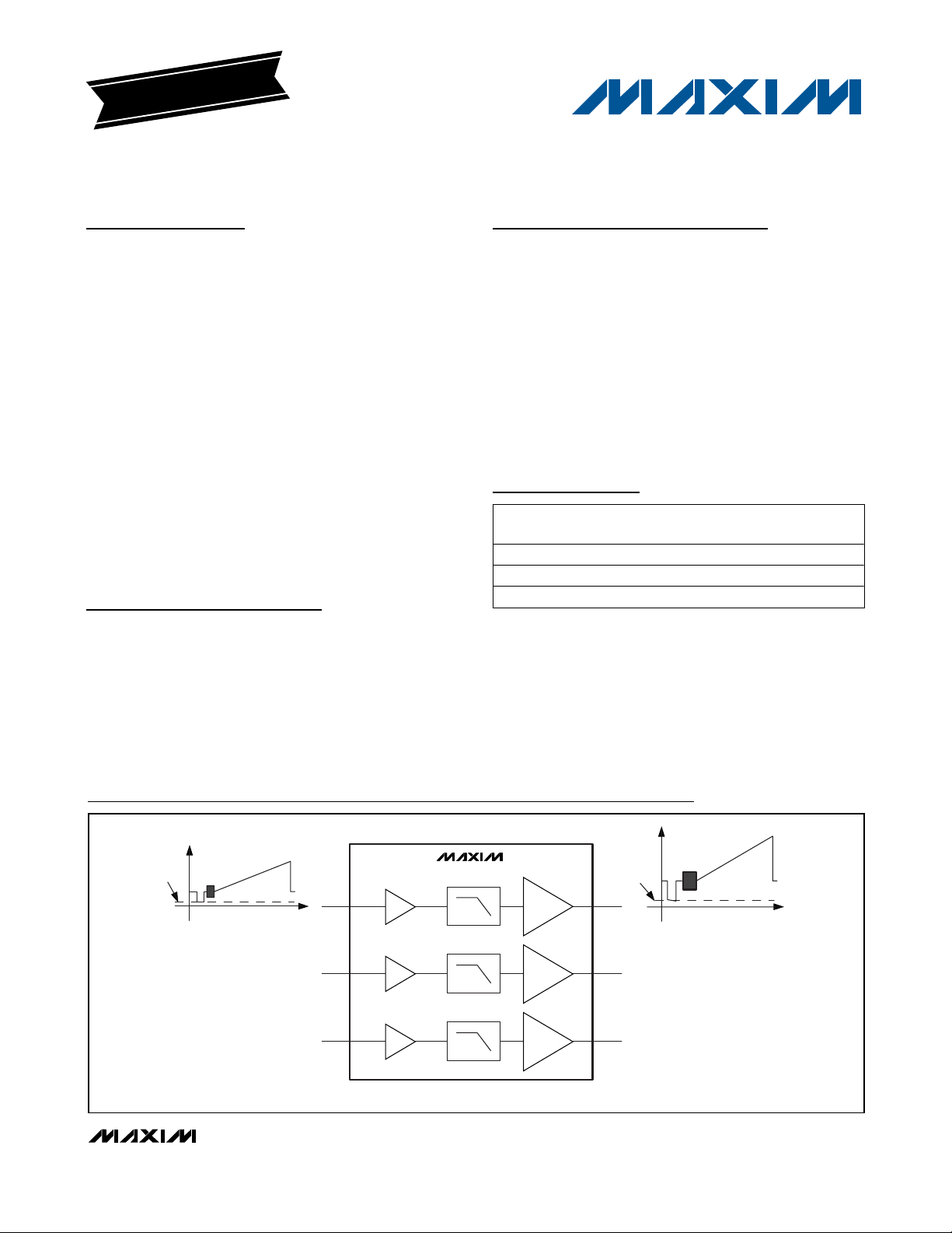
General Description
The MAX9583/MAX9584/MAX9585 are small, low-power,
multichannel video amplifiers with integrated reconstruction filters. Specially suited for standard-definition video
signals, these devices are ideal for a wide range of
television, set-top box, and portable applications.
The MAX9583/MAX9584/MAX9585 inputs can be
directly connected to the outputs of a video digital-toanalog converter (DAC). The reconstruction filter typically has ±1dB passband flatness at 8.5MHz and 55dB
attenuation at 27MHz. The amplifiers have a 2V/V gain
and the outputs can be DC-coupled to a 75Ω load which
is the equivalent of two video loads, or AC-coupled to a
150Ω load.
The MAX9583/MAX9584/MAX9585 operate from a 2.7V to
3.6V single supply and are specified over the -40°C to
+125°C automotive temperature range. The MAX9583 is
offered in a small, 6-pin thin SOT23 package. The
MAX9584 is offered in a small, 8-pin µMAX
®
package,
and the MAX9585 is offered in a small, 10-pin µMAX
package.
Applications
Set-Top Boxes
Televisions
Portable
Features
o Dual- (MAX9583), Triple- (MAX9584),
and Quad- (MAX9585) Channel Devices
o 8.5MHz, ±1dB Passband
o 55dB Attenuation at 27MHz
o Fixed Gain of 2V/V
o Low Power: 3.5mA per Channel
o 2.7V to 3.6V Single-Supply Operation
o Small SOT23 and µMAX Packages
MAX9583/MAX9584/MAX9585
Dual, Triple, and Quad Standard-Definition Video
Filter Amplifiers with DC-Coupled Input Buffers
________________________________________________________________
Maxim Integrated Products
1
Block Diagrams
19-0817; Rev 5; 10/07
For pricing, delivery, and ordering information, please contact Maxim Direct at 1-888-629-4642,
or visit Maxim’s website at www.maxim-ic.com.
EVALUATION KIT
AVAILABLE
Pin Configurations and Selector Guide located at end of
data sheet.
µMAX is a registered trademark of Maxim Integrated Products, Inc.
Ordering Information
Note: All devices are specified over the -40°C to +125°C operating temperature range.
+
Denotes a lead-free package.
T = Tape and reel.
Block Diagrams continued at end of data sheet.
PART PIN-PACKAGE CHANNELS
MAX9583AZT+T 6 Thin SOT23-6
MAX9584AUA+T 8 µMAX-8
MAX9585AUB+T 10 µMAX-10
2
3
4
PKG
CODE
Z6+1
U8+1
U10+2
0
TO
50mV
INA
INB
INC
BUFFER
BUFFER
BUFFER
MAX9584
LPF
LPF
LPF
AV = 2V/V
AV = 2V/V
AV = 2V/V
OUTA
OUTB
OUTC
300mV
TO 400mV
MAX9583/MAX9584/MAX9585
Dual, Triple, and Quad Standard-Definition Video
Filter Amplifiers with DC-Coupled Input Buffers
2 _______________________________________________________________________________________
ABSOLUTE MAXIMUM RATINGS
ELECTRICAL CHARACTERISTICS
(V
DD
= 3.3V, GND = 0V, RL= no load, TA= T
MIN
to T
MAX
, unless otherwise noted. Typical values are at TA= +25°C) (Note 1)
Stresses beyond those listed under “Absolute Maximum Ratings” may cause permanent damage to the device. These are stress ratings only, and functional
operation of the device at these or any other conditions beyond those indicated in the operational sections of the specifications is not implied. Exposure to
absolute maximum rating conditions for extended periods may affect device reliability.
VDDto GND..............................................................-0.3V to +4V
IN_ to GND ...............................................................-0.3V to +4V
OUT_ Short-Circuit Duration to V
DD
, GND.................Continuous
Continuous Input Current
IN_ ................................................................................±20mA
Continuous Power Dissipation (T
A
= +70°C)
6-Pin Thin SOT23 (derate 9.1mW/°C above +70°C)....727mW
8-Pin µMAX (derate 4.5mW/°C above +70°C) .............362mW
10-Pin µMAX (derate 5.6mW/°C above +70°C) ...........444mW
Operating Temperature Range .........................-40°C to +125°C
Junction Temperature......................................................+150°C
Storage Temperature Range .............................-65°C to +150°C
Lead Temperature (soldering, 10s) .................................+300°C
PARAMETER SYMBOL CONDITIONS MIN TYP MAX UNITS
Supply Voltage Range V
Supply Current I
Input Voltage Range V
Input Current I
Input Resistance R
DD
DD
IN
IN
IN
DC Voltage Gain (Note 2) Av RL = 150Ω to GND
DC Gain Matching Guaranteed by DC voltage gain -2 0 +2 %
Output Level Measured at V
Output-Voltage Swing
Output Short-Circuit
Current
Output Resistance R
Power-Supply Rejection
Ratio
OUT
PSRR
Guaranteed by PSRR 2.7 3.6 V
Per channel 3.5 7 mA
Guaranteed by DC
voltage gain
VIN = 0V 0.6 10 µA
, V
OUT
IN
Measured at output, V
R
= 150Ω to -0.2V
L
Measured at output, V
= 150Ω to VDD/2
R
L
Measured at output, V
R
= 150Ω to -0.2V
L
Measured at output, V
= 150Ω to VDD/2
R
L
M easur ed at outp ut, V
R
= 75Ω to - 0.2V
L
D D
Short to GND (sourcing) 140
Short to V
V
OUT
2.7V ≤ V
f = 1MHz, 100mV
(sinking) 70
DD
= 1.5V, -10mA ≤ I
≤ 3.6V 48
DD
P-P
VDD = 2.7V 0 1.05
= 3V 0 1.2
V
DD
25 MΩ
VDD = 2.7V,
DD
IN
= 3V,
IN
≤ 1.05V
≤ 1.2V
0V ≤ V
V
0V ≤ V
1.92 2 2.04
1.92 2 2.04
= 0V, RL = 150Ω to GND 0.210 0.300 0.410 V
= 2.7V, 0V ≤ VIN ≤ 1.05V,
DD
= 2.7V, 0V ≤ VIN ≤ 1.05V,
DD
= 3V, 0V ≤ VIN ≤ 1. 2V,
DD
= 3V, 0V ≤ VIN ≤ 1. 2V,
DD
= 3.135V , 0V ≤ V
≤ 10mA 0.2 Ω
LOAD
≤ 1.05V ,
I N
2.1
2.1
2.4
2.4
2.1
29
V
V/V
V
mA
P-P
P-P
dB
MAX9583/MAX9584/MAX9585
Dual, Triple, and Quad Standard-Definition Video
Filter Amplifiers with DC-Coupled Input Buffers
_______________________________________________________________________________________ 3
ELECTRICAL CHARACTERISTICS (continued)
(V
DD
= 3.3V, GND = 0V, RL= no load, TA= T
MIN
to T
MAX
, unless otherwise noted. Typical values are at TA= +25°C) (Note 1)
Note 1: All devices are 100% production tested at TA= +25°C. Specifications over temperature limits are guaranteed by design.
Note 2: Voltage gain (A
V
) is a two-point measurement in which the output voltage swing is divided by the input voltage swing.
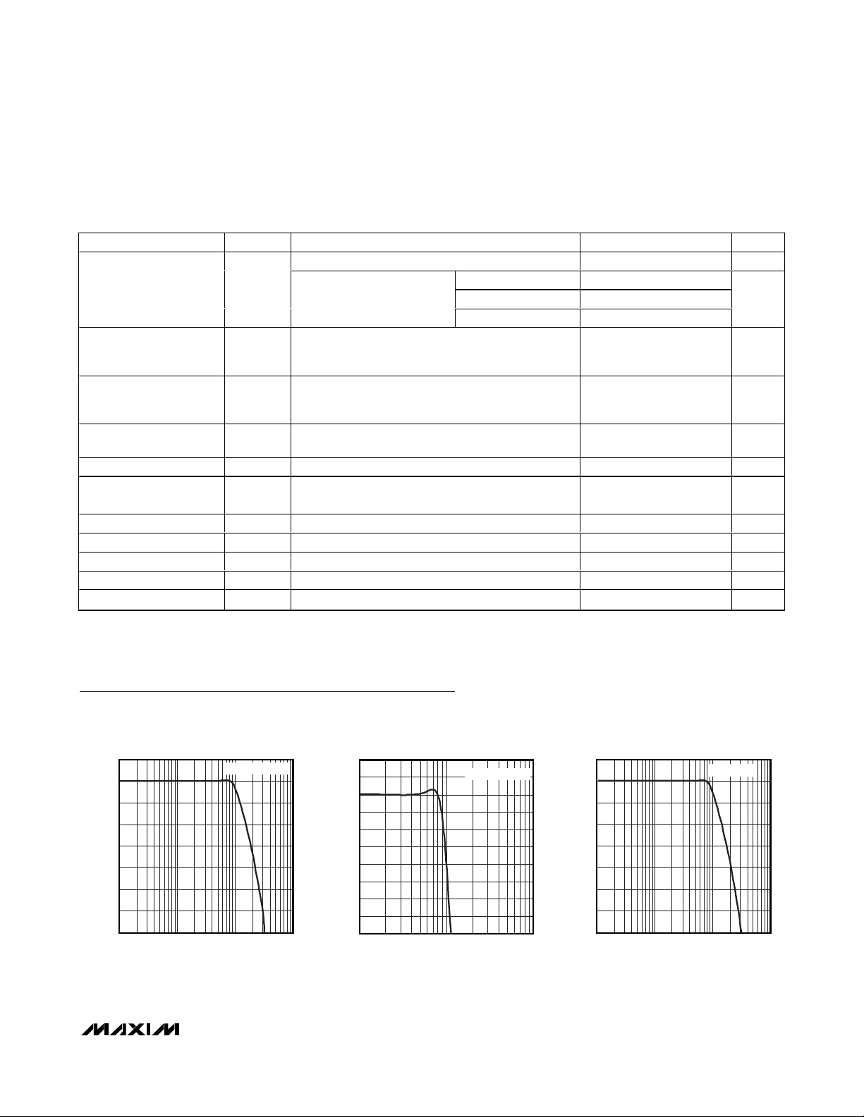
SMALL-SIGNAL GAIN
vs. FREQUENCY
MAX9583 toc01
FREQUENCY (Hz)
GAIN (dB)
10M1M
-60
-50
-40
-30
-20
-10
0
10
-70
100k 100M
V
OUT
= 100mV
P-P
SMALL-SIGNAL GAIN FLATNESS
vs. FREQUENCY
MAX9853 toc02
FREQUENCY (Hz)
GAIN (dB)
10M
-7
-6
-5
-4
-3
-2
-1
0
1
2
-8
1M 100M
V
OUT
= 100mV
P-P
LARGE-SIGNAL GAIN
vs. FREQUENCY
MAX9583 toc03
FREQUENCY (Hz)
GAIN (dB)
10M1M
-60
-50
-40
-30
-20
-10
0
10
-70
100k 100M
V
OUT
= 2V
P-P
Typical Operating Characteristics
(VDD= SHDN = 3.3V, video outputs have RL = 150Ω connected to GND, TA= +25°C, unless otherwise noted.)
PARAMETER SYMBOL CONDITIONS MIN TYP MAX UNITS
Standard-Definition
Reconstruction Filter
Differential Gain DG
Differential Phase DP
2T Pulse-to-Bar K Rating
2T Pulse Response 2T = 200ns 0.2 K%
2T Bar Response
Nonlinearity 5-step staircase 0 %
Group Delay Distortion 100kHz ≤ f ≤ 5.5MHz, outputs are 2V
P eak S i g nal to RM S N oi se 100kHz ≤ f ≤ 5.5MHz 71 dB
Output Impedance f = 5.5MHz 4.8 Ω
All Hostile Crosstalk f = 4.43MHz -64 dB
±1dB passband flatness 8.5 MHz
f = 5.5MHz -0.15
V
= 1V
IN
frequency is 100kHz
, reference
P-P
f = 9.5MHz -3
f = 27MHz -55
5-step modulated staircase of 129mV step size and
286mV peak-to-peak subcarrier amplitude,
0.1 %
f = 4.43MHz
5-step modulated staircase of 129mV step size and
286mV peak-to-peak subcarrier amplitude,
0.4 D eg r ees
f = 4.43MHz
2T = 200ns, bar time is 18µs. The beginning 2.5%
and the ending 2.5% of the bar time are ignored
2T = 200ns, bar time is 18µs. The beginning 2.5%
and the ending 2.5% of the bar time are ignored
P-P
0.6 K%
0.2 K%
9ns
dB
MAX9583/MAX9584/MAX9585
Dual, Triple, and Quad Standard-Definition Video
Filter Amplifiers with DC-Coupled Input Buffers
4 _______________________________________________________________________________________
Typical Operating Characteristics (continued)
(VDD= SHDN = 3.3V, video outputs have RL = 150Ω connected to GND, TA= +25°C, unless otherwise noted.)
LARGE-SIGNAL GAIN FLATNESS
vs. FREQUENCY
MAX9853 toc04
120
100
80
60
DELAY (ns)
40
20
0
100k 100M
2
1
0
-1
-2
-3
GAIN (dB)
-4
-5
-6
-7
-8
1M 100M
10M
FREQUENCY (Hz)
V
OUT
= 2V
P-P
QUIESCENT SUPPLY CURRENT
vs. TEMPERATURE
15.0
14.5
14.0
13.5
13.0
QUIESCENT SUPPLY CURRENT (mA)
12.5
12.0
-50 125
TEMPERATURE (°C)
1007550250-25
MAX9583 toc07
VOLTAGE GAIN (V/V)
2.04
2.03
2.02
2.01
2.00
1.99
1.98
1.97
1.96
1.95
-50 125
GROUP DELAY
vs. FREQUENCY
10M1M
FREQUENCY (Hz)
VOLTAGE GAIN
vs. TEMPERATURE
TEMPERATURE (°C)
POWER-SUPPLY REJECTION RATIO
vs. FREQUENCY
0
MAX9583 toc05
-10
-20
-30
-40
PSRR (dB)
-50
-60
-70
-80
10k 100k 100M
FREQUENCY (Hz)
10M1M
MAX9583 toc06
OUTPUT VOLTAGE
vs. INPUT VOLTAGE
3.5
3.0
MAX9583 toc08
2.5
2.0
1.5
1.0
OUTPUT VOLTAGE (V)
0.5
0
-0.5
1007525 500-25
-0.3 1.8
INPUT VOLTAGE (V)
MAX9583 toc09
1.51.20 0.3 0.6 0.9
DIFFERENTIAL GAIN AND PHASE
0.1
0
-0.1
-0.2
-0.3
DIFFERENTIAL GAIN (%)
-0.4
0.8
0.6
0.4
0.2
0
-0.2
-0.4
DIFFERENTIAL PHASE (deg)
17
f = 4.43MHz
MAX9583 toc10
6543217
f = 4.43MHz
65432
2T RESPONSE
100ns/div
MAX9583 toc11
IN_
200mV/div
OUT_
400mV/div
12.5T RESPONSE
400ns/div
MAX9583 toc12
IN_
200mV/div
OUT_
400mV/div
MAX9583/MAX9584/MAX9585
Dual, Triple, and Quad Standard-Definition Video
Filter Amplifiers with DC-Coupled Input Buffers
_______________________________________________________________________________________
5
Typical Operating Characteristics (continued)
(VDD= SHDN = 3.3V, video outputs have RL = 150Ω connected to GND, TA= +25°C, unless otherwise noted.)
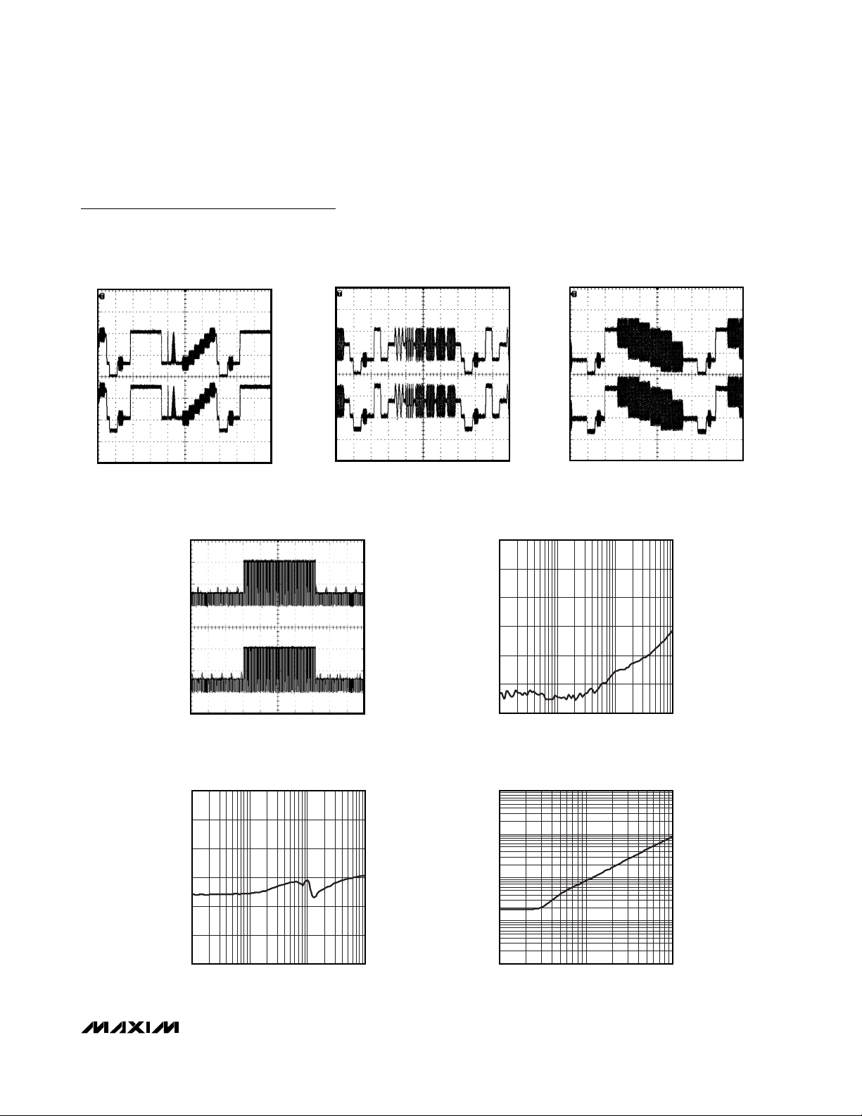
NTC-7 VIDEO TEST
SIGNAL ON CVBS OUTPUTS
MAX9583 toc13
10µs/div
OUT_
1V/div
IN_
500mV/div
PAL MULTIBURST RESPONSE
MAX9583 toc14
10µs/div
OUT_
1V/div
IN_
500mV/div
PAL COLOR BARS
MAX9583 toc15
10µs/div
OUT_
1V/div
IN_
500mV/div
FIELD SQUARE-WAVE RESPONSE
MAX9583 toc16
2ms/div
OUT_
1V/div
IN_
500mV/div
INPUT-TO-INPUT CROSSTALK
vs. FREQUENCY
MAX9583 toc17
FREQUENCY (Hz)
GAIN (dB)
10M1M
-100
-80
-60
-40
-20
0
-120
100k 100M
OUTPUT-TO-OUTPUT CROSSTALK
vs. FREQUENCY
MAX9583 toc18
FREQUENCY (Hz)
GAIN (dB)
10M1M
-100
-80
-60
-40
-20
0
-120
100k 100M
OUTPUT IMPEDANCE
vs. FREQUENCY
MAX9586 toc19
FREQUENCY (Hz)
OUTPUT IMPEDANCE (Ω)
1M
0.1
1
10
100
0.01
100k 10M

MAX9583/MAX9584/MAX9585
Dual, Triple, and Quad Standard-Definition Video
Filter Amplifiers with DC-Coupled Input Buffers
6 _______________________________________________________________________________________
Pin Description
Typical Application Circuits
MAX9583 MAX9584 MAX9585
6 SOT23 8 µMAX 10 µMAX
2 4 5 GND Ground
3 1 1 INA Video Input A
1 2 2 INB Video Input B
— 3 3 INC Video Input C
— — 4 IND Video Input D
4 7 9 OUTA Video Output A
6 6 8 OUTB Video Output B
— 5 7 OUTC Video Output C
— — 6 OUTD Video Output D
5 8 10 V
NAME FUNCTION
DD
Positive Power Supply. Bypass to GND with a 0.1µF capacitor.
GRAPHICS PROCESSING
UNIT OR
MPEG DECODER
DAC
DAC
CHROMA
LUMA
MAX9583
BUFFER
INA
LPF
BUFFER
INB
LPF
AV = 2V/V
AV = 2V/V
V
DD
GND
OUTA
OUTB
+3.3V
0.1µF
75Ω
Y
75Ω
C

MAX9583/MAX9584/MAX9585
Dual, Triple, and Quad Standard-Definition Video
Filter Amplifiers with DC-Coupled Input Buffers
_______________________________________________________________________________________ 7
Typical Application Circuits (continued)
GRAPHICS PROCESSING
UNIT OR
MPEG DECODER
DAC
DAC
CHROMA
DAC
GRAPHICS PROCESSING
UNIT OR
MPEG DECODER
DAC
LUMA
CVBS
V
DD
MAX9584
BUFFER
INA
LPF
BUFFER
INB
LPF
BUFFER
INC
LPF
AV = 2V/V
AV = 2V/V
AV = 2V/V
MAX9585
BUFFER
R
INA
LPF
AV = 2V/V
GND
OUTA
OUTB
OUTC
V
DD
GND
OUTA
75Ω
75Ω
75Ω
75Ω
+3.3V
0.1µF
Y
C
CVBS
+3.3V
0.1µF
R
BUFFER
DAC
DAC
DAC
CVBS
G
B
INB
INC
IND
BUFFER
BUFFER
LPF
LPF
LPF
AV = 2V/V
AV = 2V/V
AV = 2V/V
OUTB
OUTC
OUTD
75Ω
75Ω
75Ω
G
B
CVBS

MAX9583/MAX9584/MAX9585
Dual, Triple, and Quad Standard-Definition Video
Filter Amplifiers with DC-Coupled Input Buffers
8 _______________________________________________________________________________________
Detailed Description
The MAX9583/MAX9584/MAX9585 filter and amplify the
video DAC output in applications such as set-top boxes
and televisions. These devices consist of input buffers,
lowpass filters, and gain of 2V/V output amplifiers capable of driving a standard 150Ω video load to ground.
Inputs
The video inputs should be directly connected to the
output of the video current DAC. DC coupling ensures
that the input signals are ground referenced so that the
sync tip of composite or luma signals is within 50mV of
ground and the blank level of the chroma signal is
between 0.5V and 0.65V. Since the input buffers are
identical, any standard-definition video signal can be
applied to those inputs provided the signal is between
ground and 1.05V when V
DD
= 2.7V. For example,
three composite video signals could be applied to INA,
INB, and INC of the MAX9584. The RGB set or the
YPbPr set can also be inputs to INA, INB, and INC of
the MAX9584.
Video Filter
The filter passband (±1dB) is typically 8.5MHz, which
makes the device suitable for standard-definition video
signals from all sources (e.g., broadcast and DVD).
Broadcast video signals are channel limited: NTSC signals have 4.2MHz bandwidth and PAL signals have
5MHz bandwidth. Video signals from a DVD player,
however, are not channel limited, so the bandwidth of
DVD video signals can approach the Nyquist limit of
6.75MHz. (Recommendation ITU-R BT.601-5 specifies
13.5MHz as the sampling rate for standard-definition
video). Therefore, the maximum bandwidth of the signal
is 6.75MHz. To ease the filtering requirements, most
modern video systems oversample by two times, clocking the video current DAC at 27MHz.
Outputs
The video output amplifiers can both source and sink
load current, allowing output loads to be DC- or ACcoupled. The amplifier output stage needs approximately 300mV of headroom from either supply rail. The
devices have an internal level-shift circuit that positions
the sync tip at approximately 300mV at the output. The
blank level of the chroma output is positioned at
approximately 1.3V if the blank level of the chroma
input signal is 0.5V. The blank level of the chroma output is positioned at approximately 1.5V if the blank level
of the chroma input signal is 0.6V.
If the supply voltage is greater than 3.135V (5% below
a 3.3V supply), each amplifier can drive two DC-coupled video loads to ground. If the supply is less than
3.135V, each amplifier can drive only one DC-coupled
or AC-coupled video load.
Applications Information
Reducing Power Consumption
in the Video DACs
The MAX9583/MAX9584/MAX9585 have high-impedance input buffers that work with source resistances as
high as 1000Ω. To reduce power dissipation in the
video DACs, the DAC output resistor can be scaled up
in value. The reference resistor that sets the reference
current inside the video DACs must also be similarly
scaled up. For instance, if the output resistor is 37.5Ω,
the DAC must source 26.7mA when the output is 1V. If
the output resistor is increased to 300Ω, then the DAC
only needs to source 3.33mA when the output is 1V.
There is parasitic capacitance from the DAC output to
ground. That capacitance, in parallel with the DAC output resistor, forms a pole that can potentially roll off the
frequency response of the video signal. For example,
300Ω in parallel with 50pF create a pole at 10.6MHz. To
minimize this capacitance, reduce the area of the signal trace attached to the DAC output as much as possible, and place the MAX9583/MAX9584/MAX9585 as
close as possible to the video DAC outputs.
AC-Coupling the Outputs
The outputs can be AC-coupled since the output stage
can source and sink current as shown in Figure 1.
Coupling capacitors should be 220µF or greater to
keep the highpass filter, formed by the 150Ω equivalent
resistance of the video transmission line, to a corner
frequency of 4.8Hz or below. The frame rate of PAL
systems is 25Hz, and the frame rate of NTSC systems
is 30Hz. The corner frequency should be well below the
frame rate.
Power-Supply Bypassing and Ground
The MAX9583/MAX9584/MAX9585 operate from a singlesupply voltage down to 2.7V, allowing for low-power operation. Bypass VDDto GND with a 0.1µF capacitor. Place all
external components as close as possible to the device.

MAX9583/MAX9584/MAX9585
Dual, Triple, and Quad Standard-Definition Video
Filter Amplifiers with DC-Coupled Input Buffers
_______________________________________________________________________________________ 9
Figure 1. AC-Coupled Outputs
V
GRAPHICS PROCESSING
UNIT OR
MPEG DECODER
DAC
DD
MAX9585
BUFFER
R
INA
LPF
AV = 2V/V
GND
OUTA
75Ω
+3.3V
0.1µF
220µF
R
DAC
DAC
DAC
G
B
CVBS
INB
INC
IND
BUFFER
BUFFER
BUFFER
LPF
LPF
LPF
AV = 2V/V
AV = 2V/V
AV = 2V/V
OUTB
OUTC
OUTD
75Ω
75Ω
75Ω
220µF
G
220µF
B
220µF
CVBS

MAX9583/MAX9584/MAX9585
Dual, Triple, and Quad Standard-Definition Video
Filter Amplifiers with DC-Coupled Input Buffers
10 ______________________________________________________________________________________
Block Diagrams (continued)
0mV
TO
50mV
INA
INB
0mV
TO
50mV
INA
INB
BUFFER
BUFFER
BUFFER
BUFFER
MAX9583
LPF
LPF
MAX9585
LPF
LPF
AV = 2V/V
AV = 2V/V
AV = 2V/V
AV = 2V/V
300mV
TO 400mV
OUTA
OUTB
300mV
TO 400mV
OUTA
OUTB
BUFFER
INC
IND
BUFFER
LPF
LPF
AV = 2V/V
AV = 2V/V
OUTC
OUTD

MAX9583/MAX9584/MAX9585
Dual, Triple, and Quad Standard-Definition Video
Filter Amplifiers with DC-Coupled Input Buffers
______________________________________________________________________________________ 11
Pin Configurations
Selector Guide
Note: All devices are specified over the -40°C to +125°C operating temperature range.
+
Denotes a lead-free package.
Chip Information
PROCESS: BiCMOS
TOP VIEW
+
1 6 OUTB
INB
GND
MAX9583
2
34
5V
DD
OUTAINA
INA
INB
INC
1
2
3
4
+
MAX9584
+
INA
1
8
V
DD
7
OUTA
6
OUTB
5
OUTCGND
INB
INC
2
3
MAX9585
4
5
V
10
DD
9
OUTA
8
OUTB
7
OUTCIND
6
OUTDGND
8 µMAX
10 µMAX
SOT23
PART PIN-PACKAGE PACKAGE SIZE CHANNELS TOP MARK PKG CODE
MAX9583AZT+ 6 Thin SOT23-6 2.9mm x 1.6mm 2 AADJ Z6+1
MAX9584AUA+ 8 µMAX-8 3mm x 3mm 3 — U8+1
MAX9585AUB+ 10 µMAX-10 3mm x 3mm 4 — U10+2

MAX9583/MAX9584/MAX9585
Dual, Triple, and Quad Standard-Definition Video
Filter Amplifiers with DC-Coupled Input Buffers
12 ______________________________________________________________________________________
Package Information
(The package drawing(s) in this data sheet may not reflect the most current specifications. For the latest package outline information,
go to www.maxim-ic.com/packages
.)
6L THIN SOT23.EPS

MAX9583/MAX9584/MAX9585
Dual, Triple, and Quad Standard-Definition Video
Filter Amplifiers with DC-Coupled Input Buffers
______________________________________________________________________________________ 13
Package Information (continued)
(The package drawing(s) in this data sheet may not reflect the most current specifications. For the latest package outline information,
go to www.maxim-ic.com/packages
.)

MAX9583/MAX9584/MAX9585
Dual, Triple, and Quad Standard-Definition Video
Filter Amplifiers with DC-Coupled Input Buffers
14 ______________________________________________________________________________________
Package Information (continued)
(The package drawing(s) in this data sheet may not reflect the most current specifications. For the latest package outline information,
go to www.maxim-ic.com/packages
.)
8
b
E H
A1
A
Ø0.50±0.1
0.6±0.1
0.6±0.1
1
D
TOP VIEW
A2
e
FRONT VIEW
4X S
BOTTOM VIEW
c
L
SIDE VIEW
8
1
6°
MILLIMETERS
MIN
0.05 0.15
0.25 0.36
0.13 0.18
2.95 3.05
2.95 3.05
4.78
0.41
MAX
- 1.10
0.950.75
0.65 BSC
5.03
0.66
6°0°
0.5250 BSC
8LUMAXD.EPS
DIM
A
A1
A2
b
c
D
e
E
H
L
α
S
INCHES
MIN
-
0.002
0.030
0.010
0.005
0.116
0.0256 BSC
0.116
0.188
0.016
0°
0.0207 BSC
MAX
0.043
0.006
0.037
0.014
0.007
0.120
0.120
0.198
0.026
α
PROPRIETARY INFORMATION
TITLE:
PACKAGE OUTLINE, 8L uMAX/uSOP
21-0036
REV.DOCUMENT CONTROL NO.APPROVAL
1
J
1

MAX9583/MAX9584/MAX9585
Dual, Triple, and Quad Standard-Definition Video
Filter Amplifiers with DC-Coupled Input Buffers
Maxim cannot assume responsibility for use of any circuitry other than circuitry entirely embodied in a Maxim product. No circuit patent licenses are
implied. Maxim reserves the right to change the circuitry and specifications without notice at any time.
Maxim Integrated Products, 120 San Gabriel Drive, Sunnyvale, CA 94086 408-737-7600 ____________________
15
© 2007 Maxim Integrated Products is a registered trademark of Maxim Integrated Products, Inc.
Heaney
Package Information (continued)
(The package drawing(s) in this data sheet may not reflect the most current specifications. For the latest package outline information,
go to www.maxim-ic.com/packages
.)
Revision History
Pages changed at Rev 1: 1, 2, 20
Pages changed at Rev 2: 1, 2, 6, 11–15 (deleted some
package outlines)
Pages changed at Rev 3: 1, 15
Pages changed at Rev 4: 1–4, 8, 15
Pages changed at Rev 5: 1, 8, 15
e
10
Ø0.50±0.1
0.6±0.1
1
0.6±0.1
TOP VIEW
D2
A2
4X S
10
DIM
A1
A2 0.030 0.037 0.75 0.95
D1
H
1
BOTTOM VIEW
E2
GAGE PLANE
A
D2
E1
E2
H
L
L1
b
e
c
S
α
INCHES
MAX
MIN
0.043
-A
0.006
0.002
0.120
0.116
0.118
0.114
0.116
0.120
0.118
0.114
0.199
0.187
0.0275
0.0157
0.037 REF
0.007
0.0106
0.0197 BSC
0.0035
c
0.0078
0.0196 REF
6°
0° 0° 6°
MILLIMETERS
1.10
-
0.15
3.05
3.00
3.05
3.00
5.05
0.70
0.940 REF
0.270
0.500 BSC
0.200
0.498 REF
MAX
MIN
0.05
2.95
2.89
2.95
2.89
4.75
0.40
0.177
0.090
10LUMAX.EPS
b
D1
FRONT VIEW
A1
α
E1
SIDE VIEW
L
L1
PROPRIETARY INFORMATION
TITLE:
PACKAGE OUTLINE, 10L uMAX/uSOP
REV.DOCUMENT CONTROL NO.APPROVAL
21-0061
1
1
 Loading...