

Page 1
General Description
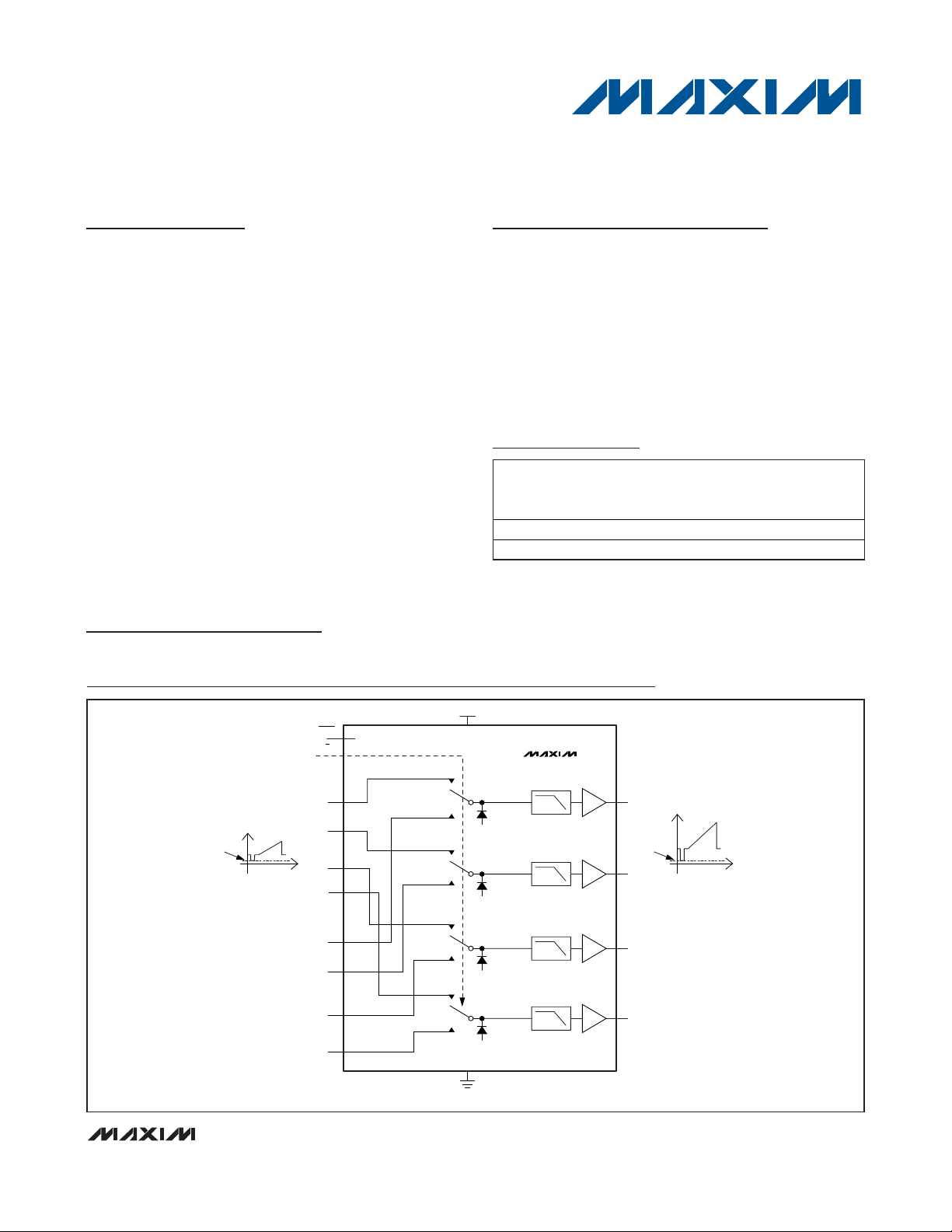
The MAX9541/MAX9542 are quadruple-channel, 2:1
video mux amplifiers with input sync tip clamps. These
devices select between two video sources and support
up to four channels on each source. The MAX9541 has
integrated lowpass filters that are optimized for standarddefinition video signals such as composite and red,
green, blue (RGB). The filters typically have ±1dB passband flatness out to 9.5MHz and 47dB attenuation at
27MHz. The MAX9542 has a wider bandwidth of 15MHz
because it does not have integrated lowpass filters, making it suitable for not only standard-definition video signals, but also video graphics array (VGA) signals with a
640 x 480 resolution at up to 85Hz refresh rate.
Video signals are AC-coupled to the inputs of the
MAX9541/MAX9542. The input sync-tip clamps set the
internal DC level.
The amplifiers have 2V/V gain, and the outputs can be
DC-coupled to a 75Ω load, which is the equivalent of two
video loads, or AC-coupled to a 150Ω load.
Both the MAX9541/MAX9542 feature a low-power shutdown mode, in which supply current is reduced to 35µA.
Applications
Automotive Infotainment
Features
♦ Quad 2:1 Video Mux Amplifiers
♦ Reconstruction Filters with 9.5MHz Passband and
47dB Attenuation at 27MHz (MAX9541)
♦ Fixed Gain of 2V/V
♦ Input Sync-Tip Clamps
♦ Shutdown
♦ 2.7V to 3.6V Single-Supply Operation
MAX9541/MAX9542
Quadruple, 2:1, Mux Amplifiers for
Standard-Definition and VGA Signals
________________________________________________________________
Maxim Integrated Products
1
19-4457; Rev 0; 2/09
For pricing, delivery, and ordering information, please contact Maxim Direct at 1-888-629-4642,
or visit Maxim’s website at www.maxim-ic.com.
UNKNOWN
BIAS
300mV
IN2A
IN3A
OUT1
IN1A
IN0A
OUT0
OUT3
OUT2
IN3B
IN2B
IN1B
IN0B
A/B
0
1
0
1
0
1
0
1
V
DD
GND
MAX9541
MAX9542
SHDN
LPF*
CLAMPREF
2V/V
LPF*
CLAMPREF
2V/V
LPF*
CLAMPREF
2V/V
LPF*
CLAMPREF
2V/V
*LOWPASS FILTER IN MAX9541 ONLY.
Functional Diagram
Ordering Information
Note: All devices are specified over the -40°C to +125°C operating temperature range.
+
Denotes a lead(Pb)-free/RoHS-compliant package.
STANDARD-
PART PIN-PACKAGE
MAX9541AEE+ 16 QSOP Yes
MAX9542AEE+ 16 QSOP No
DEFINITION
VIDEO FILTER
Page 2
MAX9541/MAX9542
Quadruple, 2:1, Mux Amplifiers for
Standard-Definition and VGA Signals
2 _______________________________________________________________________________________
ABSOLUTE MAXIMUM RATINGS
ELECTRICAL CHARACTERISTICS
(VDD= 3.3V, V
GND
= 0,
SHDN
= VDD,
A/B
= VDD, RL= 150Ω to GND, TA= T
MIN
to T
MAX
, unless otherwise noted. Typical values are
at T
A
= +25°C.) (Note 1)
Stresses beyond those listed under “Absolute Maximum Ratings” may cause permanent damage to the device. These are stress ratings only, and functional
operation of the device at these or any other conditions beyond those indicated in the operational sections of the specifications is not implied. Exposure to
absolute maximum rating conditions for extended periods may affect device reliability.
Supply Voltage
V
DD
to GND..........................................................-0.3V to +4V
Input Pins, SHDN, A/B .............................(GND - 0.3V) to +4V
Duration of Output Short Circuit to V
DD
or GND ........Continuous
Continuous Input Current
Input Pins......................................................................±20mA
Continuous Power Dissipation (T
A
= +70°C)
16-Pin QSOP (derate 8.3mW/°C above +70°C)...........667mW
Operating Temperature Range .........................-40°C to +125°C
Junction Temperature......................................................+150°C
Storage Temperature Range .............................-65°C to +150°C
Lead Temperature (soldering, 10s) .................................+300°C
Supply Voltage Range V
Quiescent Supply Current I
Shutdown Supply Current I
Input Voltage Unselected input VDD/3 V
Input Resistance Unselected input 222 kΩ
Sync-Tip Clamp Level V
Input Voltage Range
Sync Crush
Input Clamping Current 12µA
Maximum Input Source
Resistance
DC Voltage Gain (Note 2) A
DC Gain Mismatch Guaranteed by DC voltage gain -2 +2 %
Output Level Measured at V
Output Voltage Swing
Output Short-Circuit Current
Output Resistance R
PARAMETER SYMBOL CONDITIONS MIN TYP MAX UNITS
DD
DD
SHDN
CLP
Guaranteed by power-supply rejection test 2.7 3.3 3.6 V
No load 21 45 mA
SHDN = A/B= GND 35 70 μA
Guaranteed by DC
voltage gain
2.7V ≤ VDD ≤ 3.6V 1.05
3.0V ≤ V
≤ 3.6V 1.2
DD
Sync-tip clamp; percentage reduction in
sync pulse (0.3V
); guaranteed by input
P-P
clamping current measurement
VDD = 2.7V,
RL = 150Ω to GND
V
(Note 2)
OUT
, C
0V ≤ V
V
0V ≤ V
IN_
≤ 1.05V
IN
= 3V,
DD
≤ 1.2V
IN
= 0.1µF to GND 0.218 0.3 0.39 V
Measured at output, VDD = 2.7V, VIN =
V
CLP
to (V
+1.05V), RL = 150Ω to -0.2V
CLP
Measured at output, VDD = 2.7V, VIN =
V
CLP
to (V
+1.05V), RL = 150Ω to VDD/2
CLP
Measured at output, VDD = 3.0V, VIN =
V
CLP
to (V
+1.2V), RL = 150Ω to -0.2V
CLP
Measured at output, VDD = 3.0V, VIN =
V
to (V
CLP
Measured at output, V
to (V
V
CLP
+1.2V), RL = 150Ω to VDD/2
CLP
= 3.135V, VIN =
+1.05V), RL = 75Ω to -0.2V
CLP
DD
Short to GND (sourcing) 140
(sinking) 70
DD
= 1.5V, -10mA ≤ I
≤ +10mA 0.2 Ω
LOAD
OUT
Short to V
V
OUT
0.23 0.3 0.39 V
2%
300 Ω
1.96 2 2.04
1.96 2 2.04
2.1
2.1
2.4
2.4
2.1
V
V/V
V
mA
P-P
P-P
Page 3
MAX9541/MAX9542
Quadruple, 2:1, Mux Amplifiers for
Standard-Definition and VGA Signals
_______________________________________________________________________________________ 3
ELECTRICAL CHARACTERISTICS (continued)
(VDD= 3.3V, V
GND
= 0,
SHDN
= VDD,
A/B
= VDD, RL= 150Ω to GND, TA= T
MIN
to T
MAX
, unless otherwise noted. Typical values are
at T
A
= +25°C.) (Note 1)
Note 1: All devices are 100% production tested at T
A
= +25°C. Specifications over temperature limits are guaranteed by design.
Note 2: Voltage gain (A
V
) is a two-point measurement in which the output-voltage swing is divided by the input-voltage swing.
Power-Supply Rejection Ratio
Small-Signal Bandwidth V
Large-Signal Bandwidth V
Slew Rate MAX9542 only 65 V/μs
Settling Time
Standard-Definition
Reconstruction Filter
Differential Gain DG
Differential Phase DP
Group-Delay Distortion 100kHz ≤ f ≤ 5MHz, outputs are 2V
Peak Signal to RMS Noise 100kHz ≤ f ≤ 5MHz 71 dB
2T Pulse Response 2T = 200ns 0.2 K%
2T Bar Response
2T Pulse-to-Bar K Rating
Nonlinearity 5-step staircase 0.1 %
Output Impedance f = 5.5MHz 8.07 Ω
All-Hostile Crosstalk
Output-to-Input Crosstalk f = 30MHz -68 dB
LOGIC SIGNALS (TV_SEL, VCR_SEL, SHDN)
Logic-Low Threshold V
Logic-High Threshold V
Logic-Input Current I
PARAMETER SYMBOL CONDITIONS MIN TYP MAX UNITS
2.7V ≤ VDD ≤ 3.6V 48 64
f = 100kHz, 100mV
= 100mV
OUT
= 2V
OUT
Settled to within 0.1% of final value
(MAX9542 only)
V
= 2V
OUT
100kHz, ±1dB passband flatness
(MAX9541 only)
V
= 2V
OUT
frequency is 100kHz
(MAX9541 only)
5-step modulated staircase of 129mV step
size and 286mV peak-to-peak subcarrier
amplitude, f = 4.43MHz
5-step modulated staircase of 129mV step
size and 286mV peak-to-peak subcarrier
amplitude, f = 4.43MHz
2T = 200ns; bar time is 18μs; the beginning
2.5%, and the ending 2.5% of the bar time
is ignored
2T = 200ns; bar time is 18μs; the beginning
2.5%, and the ending 2.5% of the bar time
is ignored
f = 15kHz -82
f = 4.43MHz -78
IL
IH
IN
P-P
(MAX9542 only) 15 MHz
P-P
, reference frequency is
P-P
, reference
P-P
P-P
(MAX9542 only) 27 MHz
f = 5.5MHz 0.1
f = 9.5MHz -1
f = 10MHz -3
f = 27MHz -47
20
75 ns
9.5 MHz
0.4 %
0.45 deg
P-P
0.7 x
V
DD
9ns
0.2 K%
0.3 K%
0.3 x
V
DD
10 μA
dB
dB
dB
V
V
Page 4
MAX9541/MAX9542
Quadruple, 2:1, Mux Amplifiers for
Standard-Definition and VGA Signals
4 _______________________________________________________________________________________
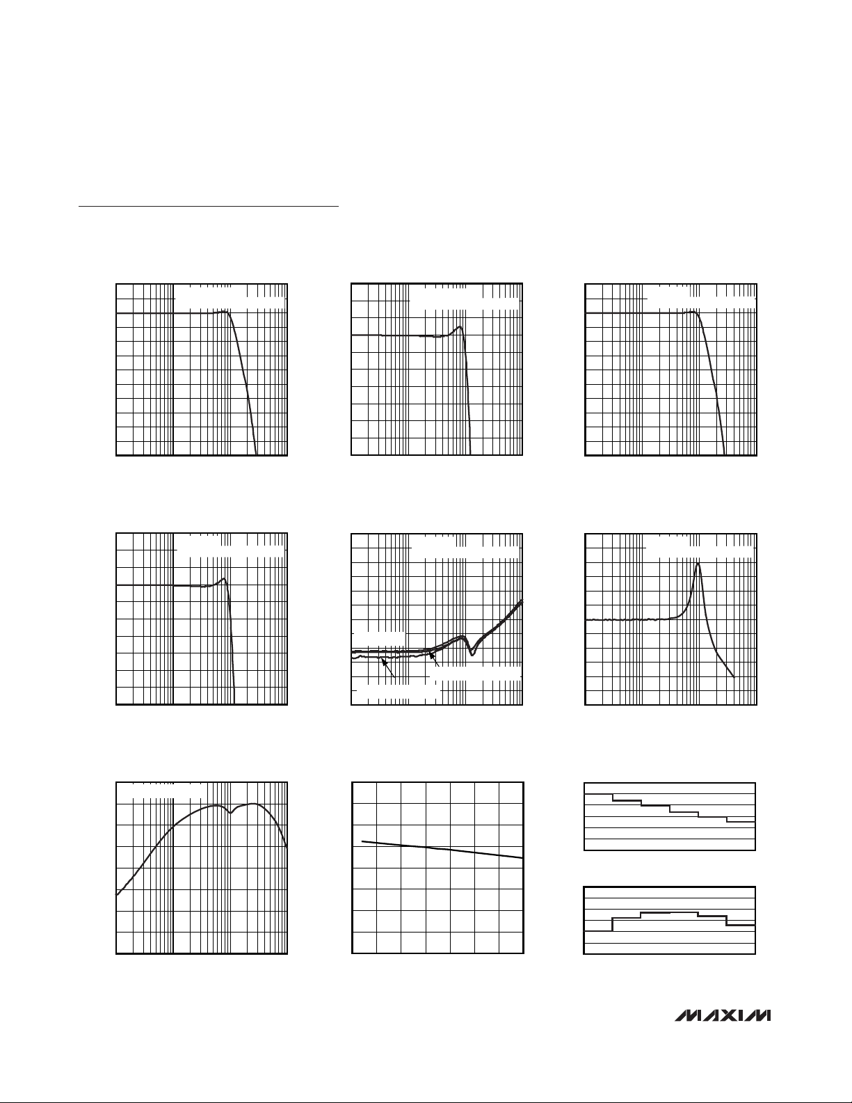
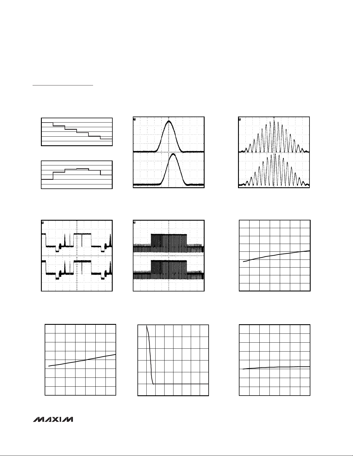
Typical Operating Characteristics (MAX9541)
(VDD= 3.3V, V
GND
= 0,
SHDN
= VDD, A/B = VDD, RL= 150Ω to GND, TA= +25°C.)
SMALL-SIGNAL GAIN
vs. FREQUENCY
MAX9541 toc01
FREQUENCY (Hz)
GAIN (dB)
10M1M
-45
-40
-35
-30
-25
-20
-15
-10
-5
0
5
10
-50
100k 100M
VIN = 50mV
P-P
GAIN IS NORMALIZED TO 0dB
SMALL-SIGNAL GAIN FLATNESS
vs. FREQUENCY
MAX9541 toc02
FREQUENCY (Hz)
GAIN (dB)
10M1M
-6
-5
-4
-3
-2
-1
0
1
2
3
-7
100k 100M
VIN = 50mV
P-P
GAIN IS NORMALIZED TO 0dB
LARGE-SIGNAL GAIN
vs. FREQUENCY
MAX9541 toc03
FREQUENCY (Hz)
GAIN (dB)
10M1M
-45
-40
-35
-30
-25
-20
-15
-10
-5
0
5
10
-50
100k 100M
VIN = 1V
P-P
GAIN IS NORMALIZED TO 0dB
LARGE-SIGNAL GAIN FLATNESS
vs. FREQUENCY
MAX9541 toc04
FREQUENCY (Hz)
GAIN (dB)
10M1M
-6
-5
-4
-3
-2
-1
0
1
2
3
-7
100k 100M
VIN = 1V
P-P
GAIN IS NORMALIZED TO 0dB
VIDEO CROSSTALK
vs. FREQUENCY
MAX9541 toc05
FREQUENCY (Hz)
GAIN (dB)
10M1M
-100
-80
-60
-40
-20
0
-120
100k 100M
ALL-HOSTILE
1 ADJACENT CHANNEL
2 ADJACENT CHANNELS
VIN = 1V
P-P
GAIN IS NORMALIZED TO 0dB
VIDEO GROUP DELAY DISTORTION
vs. FREQUENCY
MAX9541 toc06
FREQUENCY (Hz)
GROUP DELAY (ns)
10M1M
10
20
30
40
50
60
70
80
90
100
110
120
0
100k 100M
VIN = 1V
P-P
GAIN IS NORMALIZED TO 0dB
VIDEO PSRR
vs. FREQUENCY
MAX9541 toc07
FREQUENCY (Hz)
PSRR (dB)
10M1M
-70
-60
-50
-40
-30
-20
-10
0
-80
100k 100M
VDD = 3.3V + 100mV
P-P
VOLTAGE GAIN
vs. TEMPERATURE
MAX9541 toc08
TEMPERATURE (°C)
VOLTAGE GAIN (V/V)
10075-25 0 25 50
1.97
1.98
1.99
2.00
2.01
2.02
2.03
2.04
1.96
-50 125
DIFFERENTIAL GAIN
MAX9541 toc09
DIFFERENTIAL PHASE (deg)
103245
0.6
0.8
0.4
0.2
0
-0.2
-0.4
DIFFERENTIAL GAIN (%)
0
0.1
-0.1
-0.2
-0.3
-0.4
-0.5
DIFFERENTIAL PHASE
103245
f = 3.58MHz
f = 3.58MHz
Page 5
MAX9541/MAX9542
Quadruple, 2:1, Mux Amplifiers for
Standard-Definition and VGA Signals
_______________________________________________________________________________________ 5
Typical Operating Characteristics (continued) (MAX9541)
(VDD= 3.3V, V
GND
= 0,
SHDN
= VDD, A/B = VDD, RL= 150Ω to GND, TA= +25°C.)
DIFFERENTIAL GAIN
0.1
0
-0.1
-0.2
-0.3
-0.4
-0.5
DIFFERENTIAL GAIN (%)
103245
DIFFERENTIAL PHASE
0.8
0.6
0.4
0.2
0
-0.2
-0.4
DIFFERENTIAL PHASE (deg)
103245
NTC-7 VIDEO TEST SIGNAL
10
12.5T RESPONSE
400ns/div
VIDEO SYNC-TIP CLAMP VOLTAGE
vs. TEMPERATURE
TEMPERATURE (°C)
μs/div
f = 4.43MHz
f = 4.43MHz
MAX9541 toc13
MAX9541 toc10
IN
500mV/div
OUT
1V/div
2T RESPONSE
100ns/div
FIELD SQUARE WAVE
2ms/div
MAX9541 toc11
MAX9541 toc14
IN
200mV/div
OUT
400mV/div
IN
500mV/div
OUT
1V/div
0.37
0.36
0.35
0.34
0.33
0.32
0.31
0.30
SYNC-TIP CLAMP VOLTAGE (V)
0.29
0.28
-50 125
MAX9541 toc12
1007525 500-25
IN
200mV/div
OUT
400mV/div
MAX9541 toc15
VIDEO SYNC-TIP CLAMP CURRENT
vs. TEMPERATURE
1.06
1.04
1.02
1.00
0.98
0.96
0.94
SYNC-TIP CLAMP CURRENT (μA)
0.92
0.90
-50 125
TEMPERATURE (°C)
SYNC-TIP CLAMP CURRENT
vs. INPUT VOLTAGE
500
400
MAX9541 toc16
300
200
100
SYNC-TIP CLAMP CURRENT (μA)
0
10075-25 0 25 50
-100
0 0.40.2 0.6 0.8 1.0 1.2 1.4 1.6
INPUT VOLTAGE (V)
MAX9541 toc17
22.0
21.5
21.0
20.5
20.0
19.5
19.0
QUIESCENT SUPPLY CURRENT (mA)
18.5
18.0
QUIESCENT SUPPLY CURRENT
vs. TEMPERATURE
-50 125
TEMPERATURE (°C)
10075-25 0 25 50
MAX9541 toc18
Page 6

MAX9541/MAX9542
Quadruple, 2:1, Mux Amplifiers for
Standard-Definition and VGA Signals
6 _______________________________________________________________________________________
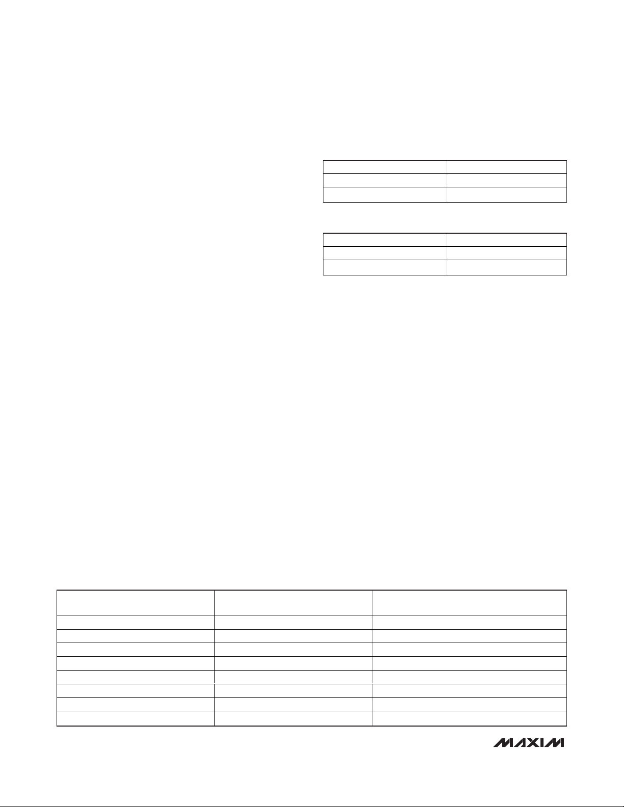
Typical Operating Characteristics (continued) (MAX9542)
(VDD= 3.3V, V
GND
= 0,
SHDN
= VDD, A/B = VDD, RL= 150Ω to GND, TA= +25°C.)
SMALL-SIGNAL GAIN
vs. FREQUENCY
10
5
0
-5
-10
-15
-20
GAIN (dB)
-25
-30
-35
-40
-45
-50
100k 100M
VIN = 50mV
P-P
GAIN IS NORMALIZED TO 0dB
1M 10M
FREQUENCY (Hz)
LARGE-SIGNAL GAIN
vs. FREQUENCY
10
5
0
-5
-10
-15
-20
GAIN (dB)
-25
-30
-35
-40
-45
-50
100k 100M
VIN = 1V
P-P
GAIN IS NORMALIZED TO 0dB
1M 10M
FREQUENCY (Hz)
VIDEO CROSSTALK
vs. FREQUENCY
0
-20
-40
-60
GAIN (dB)
ALL-HOSTILE
-80
1 ADJACENT CHANNEL
-100
-120
100k 100M
VIN = 1V
P-P
GAIN IS NORMALIZED TO 0dB
2 ADJACENT CHANNELS
1M 10M
FREQUENCY (Hz)
MAX9541 toc19
MAX9541 toc21
MAX9541 toc23
SMALL-SIGNAL GAIN FLATNESS
vs. FREQUENCY
3
2
1
0
-1
-2
GAIN (dB)
-3
-4
-5
-6
-7
100k 100M
VIN = 50mV
P-P
GAIN IS NORMALIZED TO 0dB
1M 10M
FREQUENCY (Hz)
LARGE-SIGNAL GAIN FLATNESS
vs. FREQUENCY
3
2
1
0
-1
-2
GAIN (dB)
-3
-4
-5
-6
-7
100k 100M
VIN = 1V
P-P
GAIN IS NORMALIZED TO 0dB
1M 10M
FREQUENCY (Hz)
VIDEO GROUP DELAY DISTORTION
vs. FREQUENCY
50
45
40
35
30
25
20
GROUP DELAY (ns)
15
10
5
0
100k 100M
VIN = 1V
P-P
GAIN IS NORMALIZED TO 0dB
1M 10M
FREQUENCY (Hz)
MAX9541 toc20
MAX9541 toc22
MAX9541 toc24
Page 7

MAX9541/MAX9542
Quadruple, 2:1, Mux Amplifiers for
Standard-Definition and VGA Signals
_______________________________________________________________________________________
7
Typical Operating Characteristics (continued) (MAX9542)
(VDD= 3.3V, V
GND
= 0,
SHDN
= VDD, A/B = VDD, RL= 150Ω to GND, TA= +25°C.)
0
-10
-20
-30
-40
PSRR (dB)
-50
-60
-70
-80
100k 100M
0.10
0.05
0.00
-0.05
-0.10
GAIN (%)
-0.15
DIFFERENTIAL
-0.20
0.8
0.6
0.4
0.2
0.0
PHASE (deg)
-0.2
DIFFERENTIAL
-0.4
VIDEO PSRR
vs. FREQUENCY
VDD = 3.3V + 100mV
P-P
1M 10M
FREQUENCY (Hz)
DIFFERENTIAL GAIN AND PHASE
120 345
0 345
12
f = 3.58MHz
f = 3.58MHz
MAX9541 toc25
MAX9541 toc27
VOLTAGE GAIN
vs. TEMPERATURE
2.04
2.03
2.02
2.01
2.00
1.99
VOLTAGE GAIN (V/V)
1.98
1.97
1.96
-50 125
TEMPERATURE (°C)
DIFFERENTIAL GAIN AND PHASE
0.10
0.05
0.00
-0.05
-0.10
GAIN (%)
-0.15
DIFFERENTIAL
-0.20
0.8
0.6
0.4
0.2
0.0
PHASE (deg)
-0.2
DIFFERENTIAL
-0.4
120 345
0 345
12
MAX9541 toc26
10075-25 0 25 50
f = 4.43MHz
MAX9541 toc28
f = 4.43MHz
27 RESPONSE
100ns/div
MAX9541 toc29
IN
200mV/div
OUT
400mV/div
12.5T RESPONSE
400ns/div
MAX9541 toc30
IN
200mV/div
OUT
400mV/div
Page 8

MAX9541/MAX9542
Quadruple, 2:1, Mux Amplifiers for
Standard-Definition and VGA Signals
8 _______________________________________________________________________________________
Typical Operating Characteristics (continued) (MAX9542)
(VDD= 3.3V, V
GND
= 0,
SHDN
= VDD, A/B = VDD, RL= 150Ω to GND, TA= +25°C.)
NTC-7 VIDEO TEST SIGNAL
MAX9541 toc31
10μs/div
IN
500mV/div
OUT
1V/div
FIELD SQUARE WAVE
MAX9541 toc32
2ms/div
IN
500mV/div
OUT
1V/div
PULSE RESPONSE
MAX9541 toc33
100ns/div
INPUT (700mV/div)OUTPUT (700mV/div)
VIDEO SYNC-TIP CLAMP VOLTAGE
vs. TEMPERATURE
MAX9541 toc34
TEMPERATURE (°C)
SYNC-TIP CLAMP VOLTAGE (V)
1007525 500-25
0.29
0.30
0.31
0.32
0.33
0.34
0.35
0.36
0.37
0.28
-50 125
VIDEO SYNC-TIP CLAMP CURRENT
vs. TEMPERATURE
MAX9541 toc35
TEMPERATURE (°C)
SYNC-TIP CLAMP CURRENT (μA)
10075-25 0 25 50
0.92
0.94
0.96
0.98
1.00
1.02
1.04
1.06
0.90
-50 125
QUIESCENT SUPPLY CURRENT
vs. TEMPERATURE
MAX9541 toc37
TEMPERATURE (°C)
QUIESCENT SUPPLY CURRENT (mA)
10075-25 0 25 50
18.5
19.0
19.5
20.0
20.5
21.0
21.5
22.0
18.0
-50 125
SYNC-TIP CLAMP CURRENT
vs. INPUT VOLTAGE
MAX9541 toc36
INPUT VOLTAGE (V)
SYNC-TIP CLAMP CURRENT (μA)
0.40.2
0
200
400
500
-100
300
100
0 1.00.80.6 1.61.41.2
Page 9

Detailed Description
The MAX9541 selects between two standard-definition
video sources that can each have up to four video signals, for example, RGB with composite sync (RGBS) or
RGB with sync-on-green. See Figure 1. It is also possible
to select between two sets of four composite video signals with blanking and sync (CVBS). With its integrated
lowpass filter (10MHz large-signal -3dB bandwidth typical), the MAX9541 can provide the anti-alias filtering
before an analog-to-digital converter (ADC) or the reconstruction filtering after a digital-to-analog converter
(DAC). The incoming video signals can have any DC
bias because the MAX9541 has input sync-tip clamps
which restore the DC level. The output amplifiers have a
gain of 2V/V. The MAX9541 operates from a single 3.3V
supply and consumes low quiescent power and low
average power. In addition, the device also has shutdown mode.
The MAX9542 is similar to the MAX9541 except that it
does not have the integrated lowpass filter. As a result,
the typical, large-signal bandwidth of the MAX9541 is
15MHz. Therefore, it can select between two video
sources that can each have up to four video signals
that are standard definition or VGA. A standard-definition signal set would be RGB with composite sync. A
VGA signal set would be RGB with a 640 x 480 resolution and up to 85Hz refresh rate. See Figure 2.
MAX9541/MAX9542
Quadruple, 2:1, Mux Amplifiers for
Standard-Definition and VGA Signals
_______________________________________________________________________________________ 9
Pin Description
PIN NAME FUNCTION
1 IN0A Video Input A Channel 0
2 IN1A Video Input A Channel 1
3 IN2A Video Input A Channel 2
4 IN3A Video Input A Channel 3
5 IN0B Video Input B Channel 0
6 IN1B Video Input B Channel 1
7 IN2B Video Input B Channel 2
8 IN3B Video Input B Channel 3
9 GND Ground
10 SHDN
11 OUT3 Video Output Channel 3
12 OUT2 Video Output Channel 2
13 OUT1 Video Output Channel 1
14 OUT0 Video Output Channel 0
15 A/B
16 V
DD
Shutdown Logic Input. Connect to GND to place the device in shutdown. Connect to V
operation.
Input Select. Connect to GND to select Video Input A as the video source. Connect to V
Video Input B as the video source.
Positive Power Supply. Bypass to GND with a 0.1µF capacitor.
for normal
DD
to select
DD
Page 10

MAX9541/MAX9542
Quadruple, 2:1, Mux Amplifiers for
Standard-Definition and VGA Signals
10 ______________________________________________________________________________________
Figure 1. The MAX9541 selects between two sources of RGB with composite sync, filters the signals, and drives the signals into a
display panel.
V
DD
NAVIGATION
COMPUTER
COMPOSITE
SYNC
RED
GREEN
COMPOSITE
SYNC
GREEN
VIDEO SOURCE
BLUE
RED
BLUE
75Ω
75Ω
75Ω
75Ω
75Ω
75Ω
75Ω
75Ω
0.1μF
0.1μF
0.1μF
0.1μF
0.1μF
0.1μF
0.1μF
0.1μF
IN0A
CLAMPREF
IN1A
CLAMPREF
IN2A
CLAMPREF
IN3A
CLAMPREF
IN0B
CLAMPREF
IN1B
CLAMPREF
IN2B
CLAMPREF
IN3B
CLAMPREF
MAX9541
LPF
LPF
LPF
LPF
2V/V
2V/V
2V/V
2V/V
OUT0
OUT1
OUT2
OUT3
75Ω
75Ω
75Ω
75Ω
DISPLAY
A/B
PANEL
COMPOSITE
SYNC
RED
GREEN
BLUE
GND
Page 11

MAX9541/MAX9542
Quadruple, 2:1, Mux Amplifiers for
Standard-Definition and VGA Signals
______________________________________________________________________________________ 11
Figure 2. The MAX9542 Selecting Between Two VGA Sources
PC NO. 1
PC NO. 2
RED
GREEN
BLUE
RED
GREEN
BLUE
NOT
USED
NOT
USED
75Ω
75Ω
75Ω
75Ω
75Ω
75Ω
75Ω
75Ω
0.1μF
0.1μF
0.1μF
0.1μF
0.1μF
0.1μF
0.1μF
0.1μF
IN0A
IN1A
IN2A
IN3A
IN0B
IN1B
IN2B
IN3B
CLAMPREF
CLAMPREF
CLAMPREF
CLAMPREF
CLAMPREF
CLAMPREF
CLAMPREF
CLAMPREF
V
DD
MAX9542
2V/V
2V/V
2V/V
2V/V
OUT0
OUT1
OUT2
OUT3
75Ω
75Ω
75Ω
75Ω
A/B
NOT
USED
MONITOR
RED
GREEN
BLUE
GND
Page 12
MAX9541/MAX9542
Operating Modes
A/B controls whether Video Input A or Video Input B is
selected. See Table 1.
SHDN controls whether the device is on or off. See
Table 2. In shutdown, the outputs are in high impedance.
Input
Each video source can provide up to four video signals.
Every video signal must be AC-coupled to the
MAX9541/MAX9542 through 0.1µF capacitors. The
MAX9541/MAX9542 have sync-tip clamps and bias circuits to restore the DC level of the video signal after the
input coupling capacitor. When a video input is selected, the input has a sync-tip clamp, which accepts
video signals that have sync pulses or that reach their
minimum level during sync. Composite video with
blanking and sync (CVBS) is an example of a video signal with sync pulses. The red, green, and blue signals
in an RGBS signal set are examples of signals that
return to their blank level during sync. The sync-tip voltage is internally set to 300mV.
When a video input is not selected, the inputs to the
MAX9541/MAX9542 do not distort the video signal in
case the video source is driving video signals to another video circuit such as a video multiplexer. The inputs
are biased at VDD/3, which is sufficiently above ground
so that the ESD diodes never forward bias as the video
signal changes. The input resistance is 220kΩ, which
presents negligible loading on the video current DAC.
The sole exception to this condition is IN3A, in which
the input circuit is always a sync-tip clamp. Table 3
summarizes which input circuit is active, dependent
upon A/B.
In shutdown mode (SHDN = LOW), a bias circuit is
active on every input.
Multiplexer
The MAX9541/MAX9542 have quadruple 2:1 multiplexers to select between either Video Input A or Video
Input B as the source of the video signal. When A/B is
connected to GND, Video Input A is the video source.
When A/B is connected to VDD, Video Input B is the
video source.
Video Filter
The MAX9541 filter features ±1dB passband out to
9.5MHz and 47dB attenuation at 27MHz, making the filter suitable for standard-definition video signals from all
sources (e.g., broadcast and DVD). Broadcast video
signals are channel limited: NTSC signals have 4.2MHz
bandwidth, and PAL signals have 5MHz bandwidth.
Video signals from a DVD player, however, are not
channel limited; so the bandwidth of DVD video signals
can approach the Nyquist limit of 6.75MHz.
Recommendation: ITU-R BT.601-5 specifies 13.5MHz
as the sampling rate for standard-definition video.
Therefore, the maximum bandwidth of the signal is
6.75MHz. To ease the filtering requirements, most modern video systems oversample by two times, clocking
the video current DAC at 27MHz.
The MAX9542 does not have a filter.
Quadruple, 2:1, Mux Amplifiers for
Standard-Definition and VGA Signals
12 ______________________________________________________________________________________
Table 1. A/B Logic
Table 2. SHDN Logic
Table 3. Input Circuit of Input as Determined by State of A/B (SHDN = HIGH)
LOGIC STATE MODE
Low Video Input A
High Video Input B
LOGIC STATE MODE
Low Off
High On
INPUT
IN0A Sync-tip clamp Bias
IN1A Sync-tip clamp Bias
IN2A Sync-tip clamp Bias
IN3A Sync-tip clamp Sync-tip clamp
IN0B Bias Sync-tip clamp
IN1B Bias Sync-tip clamp
IN2B Bias Sync-tip clamp
IN3B Bias Sync-tip clamp
INPUT CIRCUIT
A/B = LOW
INPUT CIRCUIT
A/B = HIGH
Page 13

Outputs
The video output amplifiers can both source and sink
load current, allowing output loads to be DC- or
AC-coupled. The amplifier output stage needs approximately 300mV of headroom from either supply rail. The
devices have an internal level-shift circuit that positions
the sync tip at approximately 300mV at the output.
If the supply voltage is greater than 3.135V (5% below
a 3.3V supply), each amplifier can drive two DC-coupled video loads to ground. If the supply is less than
3.135V, each amplifier can drive only one DC-coupled
or AC-coupled video load.
Applications Information
AC-Coupling the Outputs
The outputs can be AC-coupled since the output stage
can source and sink current as shown in Figure 3.
Coupling capacitors should be 220µF or greater to
keep the highpass filter, formed by the 150Ω equivalent
resistance of the video transmission line, to a corner
frequency of 4.8Hz or below. The frame rate of PAL
systems is 25Hz, the frame rate of NTSC systems is
30Hz, and the frame rate of VGA is usually 60Hz or
higher. The corner frequency should be well below the
frame rate.
Power Consumption
The quiescent power consumption and average power
consumption of the MAX9541/MAX9542 are very low
because of 3.3V operation and low-power circuit
design. Quiescent power consumption is defined when
the MAX9541/MAX9542 are operating without loads
and without any video signals.
Average power consumption represents the normal power
consumption when the devices drive real video signals
into real video loads. It is measured when the MAX9541/
MAX9542 drive 150Ω loads to ground with a 50% flat
field, which serves as proxy for a real video signal.
Table 4 shows the quiescent and average power consumption of the MAX9541/MAX9542.
Power-Supply Bypassing and Ground
The MAX9541/MAX9542 operate from a single-supply
voltage down to 2.7V, allowing for low-power operation.
Bypass V
DD
to GND with a 0.1µF capacitor. Place all
external components as close as possible to the
device.
MAX9541/MAX9542
Quadruple, 2:1, Mux Amplifiers for
Standard-Definition and VGA Signals
______________________________________________________________________________________ 13
Table 4. Quiescent and Average Power Consumption
Chip Information
PROCESS: BiCMOS
16
15
14
13
12
11
10
9
1
2
3
4
5
6
7
8
IN0A
V
DD
A/B
OUT0
OUT1
OUT2
OUT3
SHDN
GND
TOP VIEW
MAX9541
MAX9542
QSOP
IN1A
IN2A
IN1B
IN3A
IN0B
IN2B
IN3B
+
Pin Configuration
MEASUREMENT POWER CONSUMPTION (mW) CONDITIONS
Quiescent power consumption 69 No load.
Average power consumption 175
150Ω to ground on each output. 50% flat field signal on
each input.
Page 14

MAX9541/MAX9542
Quadruple, 2:1, Mux Amplifiers for
Standard-Definition and VGA Signals
14 ______________________________________________________________________________________
Figure 3. AC-Coupled Outputs
+3.3V
0.1μF
SHDN
A/B
0.1μF
IN0A
75Ω
0.1μF
IN1A
VIDEO SOURCE A
4 CVBS SIGNALS
75Ω
0.1μF
75Ω
0.1μF
75Ω
0.1μF
75Ω
0.1μF
IN2A
IN3A
IN0B
IN1B
V
DD
BUFFER
CLAMPREF
BUFFER
CLAMPREF
BUFFER
CLAMPREF
MAX9541
MAX9542
LPF*
LPF*
LPF*
2V/V
2V/V
2V/V
OUT0
OUT1
OUT2
220μF
75Ω
220μF
75Ω
220μF
75Ω
0
1
0
1
0
1
VIDEO SOURCE B
4 CVBS SIGNALS
*LOWPASS FILTER MAX9451 ONLY.
75Ω
0.1μF
75Ω
0.1μF
75Ω
IN2B
IN3B
0
BUFFER
1
CLAMPREF
LPF*
GND
2V/V
OUT3
220μF
75Ω
Page 15

MAX9541/MAX9542
Quadruple, 2:1, Mux Amplifiers for
Standard-Definition and VGA Signals
______________________________________________________________________________________ 15
Typical Application Circuit
VIDEO SOURCE A
4 CVBS SIGNALS
A/B
0.1μF
75Ω
0.1μF
75Ω
0.1μF
75Ω
0.1μF
75Ω
SHDN
IN0A
IN1A
IN2A
IN3A
+3.3V
0.1μF
V
DD
BUFFER
CLAMPREF
BUFFER
CLAMPREF
MAX9541
MAX9542
LPF*
LPF*
2V/V
2V/V
OUT0
OUT1
75Ω
75Ω
VIDEO OUTPUT
4 CVBS SIGNALS
0
1
0
1
0
VIDEO SOURCE B
4 CVBS SIGNALS
*LOWPASS FILTER MAX9451 ONLY.
0.1μF
75Ω
0.1μF
75Ω
0.1μF
75Ω
0.1μF
75Ω
IN0B
IN1B
IN2B
IN3B
BUFFER
1
CLAMPREF
0
BUFFER
1
CLAMPREF
LPF*
LPF*
GND
2V/V
2V/V
OUT2
75Ω
OUT3
75Ω
Page 16

MAX9541/MAX9542
Quadruple, 2:1, Mux Amplifiers for
Standard-Definition and VGA Signals
Maxim cannot assume responsibility for use of any circuitry other than circuitry entirely embodied in a Maxim product. No circuit patent licenses are
implied. Maxim reserves the right to change the circuitry and specifications without notice at any time.
16
____________________Maxim Integrated Products, 120 San Gabriel Drive, Sunnyvale, CA 94086 408-737-7600
© 2009 Maxim Integrated Products Maxim is a registered trademark of Maxim Integrated Products, Inc.
PACKAGE TYPE PACKAGE CODE DOCUMENT NO.
16 QSOP E16-4
21-0055
Package Information
For the latest package outline information and land patterns, go to www.maxim-ic.com/packages.
QSOP.EPS
 Loading...