

Page 1
General Description
The MAX9526 is a low-power video decoder that converts NTSC or PAL composite video signals to 8-bit or
10-bit YCbCr component video compliant with the ITUR BT.656 standard. The device powers up in fully operational mode and automatically configures itself to
decode the detected input standard. The MAX9526
typically consumes 200mW of power in normal operation and typically less than 100µW in shutdown mode.
An internal 10-bit, 54MHz analog-to-digital converter
(ADC) samples the input with four times oversampling.
The MAX9526 features a DC restoration circuit with offset correction and automatic gain control to accurately
optimize the full-scale range of the ADC.
An integrated analog anti-aliasing filter eliminates the
need for external filtering. The MAX9526 includes a 2:1
input multiplexer with automatic signal selection based
on activity at the inputs.
An internal line-locked phase-locked loop (PLL) generates the sample clock and the line-locked clock (LLC)
output to provide an ITU-compliant output. Alternatively,
the PLL can be configured to provide a sample clock
and output clock at 2x and 1x the frequency of the
crystal oscillator, respectively.
The MAX9526 provides a multiline adaptive comb filter to
reduce cross-chrominance and cross-luminance artifacts.
A single 1.8V supply is used for both the digital and
analog supplies. The digital outputs operate from a
separate +1.7V to +3.45V supply to allow direct connection to a wide range of digital processors. The
MAX9526 operates over the -40°C to +125°C automotive temperature range and is available in both a
28-pin QSOP and a 32-pin TQFN (5mm x 6mm).
Applications
Automotive Entertainment Systems
Collision Avoidance Systems
Security Surveillance/CCTV Systems
Televisions
Features
o Supports All NTSC and PAL Standards
NTSC M, NTSC J, NTSC 4.43,
PAL B/G/H/I/D, PAL M, PAL N, PAL 60
o Easy to Configure and Operate with Only
16 User-Programmable Registers
o Automatic Configuration and Standard Select
o 10-Bit 4x Oversampling (54Msps) ADC with True
10-Bit Digital Processing
o Flexible Output Formatting
10-Bit Parallel ITU-R BT.656 Output with
Embedded TRS
8-Bit Parallel ITU-R BT.656 Output with Separate
HS and VS
o +1.8V Digital and Analog Supply Voltage
o +1.7V to +3.45V Digital I/O Supply Voltage
o Full Automotive Temperature Range (-40°C to
+125°C)
o Low-Power Modes
Shutdown (< 100µW typ)
Sleep Mode with Continuous Activity Detection
(< 5mW typ)
o 2-to-1 Video Input Mux with AGC
MAX9526
Low-Power, High-Performance
NTSC/PAL Video Decoder
________________________________________________________________
Maxim Integrated Products
1
19-4535; Rev 3; 2/11
For pricing, delivery, and ordering information, please contact Maxim Direct at 1-888-629-4642,
or visit Maxim’s website at www.maxim-ic.com.
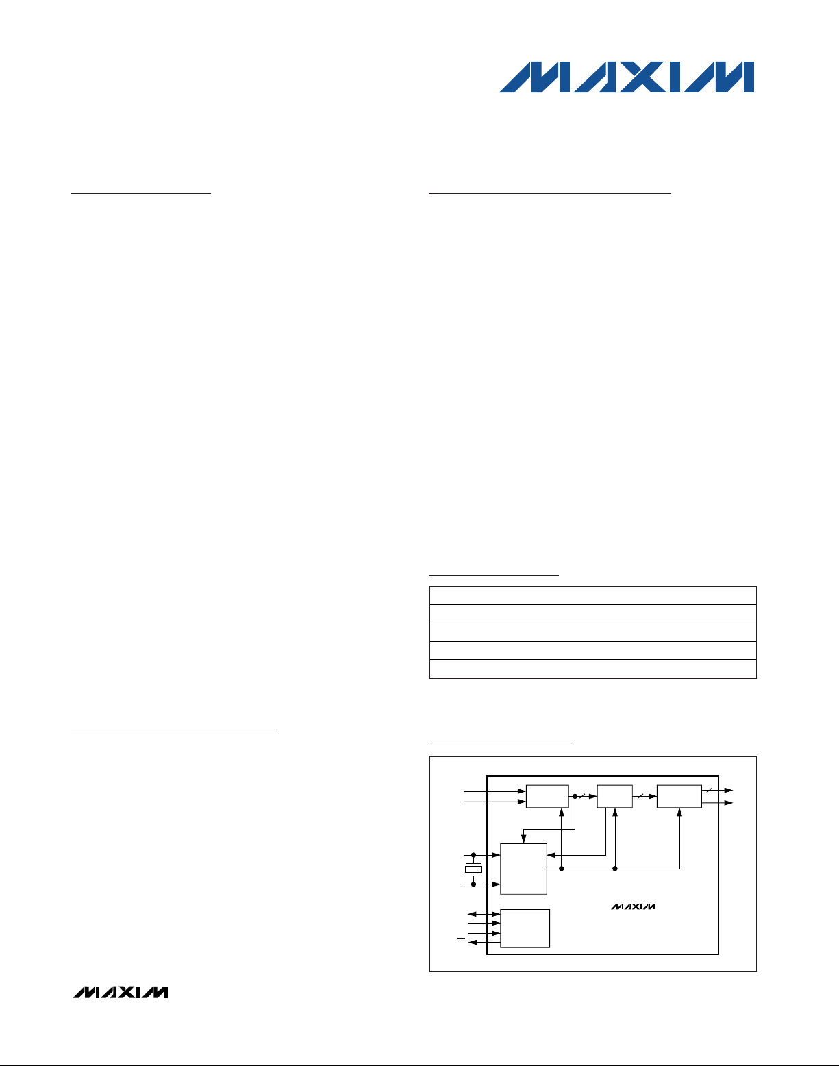
ANALOG
FRONT-END
DIGITAL
DECODER
OUTPUT
PROCESSING
SYNC
PROCESSING,
CLOCK
GENERATION,
AND PLL
I
2
C INTERFACE
AND REGISTERS
V
IN1
V
IN2
XTAL/OSC
XTAL2
SDA
SCL
DEVADDR
IRQ
D9–D0
LLC
CLOCK
10
1010
NONSTD
VIDEO
MAX9526
Functional Diagram
Ordering Information
+
Denotes lead(Pb)-free/RoHS-compliant package.
/V denotes an automotive qualified part.
*
EP = Exposed pad.
PART TEMP RANGE PIN-PACKAGE
MAX9526AEI+ -40°C to +125°C 28 QSOP
MAX9526AEI/V+ -40°C to +125°C 28 QSOP
MAX9526ATJ+ -40°C to +125°C 32 TQFN-EP*
MAX9526ATJ/V+ -40°C to +125°C 32 TQFN-EP*
Page 2
MAX9526
Low-Power, High-Performance
NTSC/PAL Video Decoder
2 _______________________________________________________________________________________
ABSOLUTE MAXIMUM RATINGS
ELECTRICAL CHARACTERISTICS
(V
AVDD
= V
DVDD
= +1.8V, V
DVDDIO
= +3.3V, V
AGND
= V
DGND
= 0V, TA= T
MIN
to T
MAX
, unless otherwise noted. Typical values are at
T
A
= +25°C.) (Note 1)
Stresses beyond those listed under “Absolute Maximum Ratings” may cause permanent damage to the device. These are stress ratings only, and functional
operation of the device at these or any other conditions beyond those indicated in the operational sections of the specifications is not implied. Exposure to
absolute maximum rating conditions for extended periods may affect device reliability.
AVDD to AGND .......................................................-0.3V to +2V
DVDD to DGND ........................................................-0.3V to +2V
DVDDIO to DGND .................................................-0.3V to +3.6V
AGND to DGND.....................................................-0.1V to +0.1V
D9–D0, LLC to DGND .........................-0.3V to (DVDDIO + 0.3V)
V
IN1
, V
IN2
, V
REF
to AGND .......................-0.3V to (AVDD + 0.3V)
XTAL/OSC, XTAL2 to AGND ....................................-0.3V to +2V
IRQ, SDA, SCL, DEVADR to DGND ......................-0.3V to +3.6V
Continuous Current In/Out All Pins ...................................±50mA
Continuous Power Dissipation (T
A
= +70°C)
28-Pin QSOP Single-Layer Board
(derate 10.8mW/°C above +70°C).............................860mW
28-Pin QSOP Multilayer Board
(derate 12.6mW°C above +70°C)............................1009mW
32-Pin TQFN Multilayer Board
(derate 20.8mW/°C above +70°C)...........................1663mW
Operating Temperature Range .........................-40°C to +125°C
Junction Temperature......................................................+150°C
Storage Temperature Range .............................-65°C to +150°C
Lead Temperature (soldering, 10s) .................................+300°C
Soldering Temperature (reflow) .......................................+260°C
SUPPLIES
Analog Supply Voltage Range AVDD 1.7 1.8 1.9 V
Digital Supply Voltage Range DVDD 1.7 1.8 1.9 V
Digital I/O Supply Voltage Range DVDDIO 1.7 3.3 3.45 V
Analog Supply Current
(Note 2)
Digital Supply Current
(Note 2)
Digital I/O Supply Current
(Note 2)
VIDEO INPUTS, V
Input Voltage Range Guaranteed by full-scale conversion range 0.27 0.5 0.83 V
Input Resistance R
Input Capacitance C
Video Input Reference Voltage
)
(V
REF
Sync-Tip Clamp Level V
Input Clamping Current
PARAMETER SYMBOL CONDITIONS MIN TYP MAX UNITS
, AND CLAMP
REF
I
AVDD
I
DVDD
I
DVDDIO
IN
IN
V
REF
CLMP2
Normal operation 42 55
Sleep mode 2.2 3
Shutdown 0.5 100 µA
Normal operation 70 110 mA
Sleep mode 5 1000
Shutdown 5 1000
Normal operation, V
Normal operation, V
Sleep mode, V
Shutdown, V
Activity detect clamp 550 mV
Activity detect clamp,
V
= V
VIN
CLMP2
DVDDIO
= 1.8V 3.5
DVDDIO
= 3.3V 6.4
DVDDIO
= 3.3V 0.8 10
DVDDIO
= 3.3V 0.8 10
+ 150mV
2MΩ
8pF
850 mV
2.0 µA
mA
µA
mA
µA
P-P
Page 3
MAX9526
Low-Power, High-Performance
NTSC/PAL Video Decoder
_______________________________________________________________________________________ 3
ELECTRICAL CHARACTERISTICS (continued)
(V
AVDD
= V
DVDD
= +1.8V, V
DVDDIO
= +3.3V, V
AGND
= V
DGND
= 0V, TA= T
MIN
to T
MAX
, unless otherwise noted. Typical values are at
T
A
= +25°C.) (Note 1)
Sync Slice Comparator Level Activity detect slicer, referenced to V
DC Restore Current DAC FullScale Range (Source and Sink)
(Note 3)
D C Restor e S ync- Ti p Level at
/V
V
IN1
IN2 AGCGAIN = 0xF, ADAGC = 1 0.72
ANALOG INPUT FILTER AND ADC (Note 4)
C utoff Fr eq uency ( 3d B) f
P assb and Fl atness
S top b and C utoff f
S top b and Attenuati on
Ful l - S cal e C onver si on Rang e
AGC Gai n S tep si ze 0.167 V/V
D i ffer enti al N onl i near i ty D N L AGCGAIN = 0x0, ADAGC = 1 ±0.5 LSB
Integ r al N onl i near i ty IN L AGCGAIN = 0x0, ADAGC = 1 ±1 LSB
S i g nal - to- N oi se Rati oS N R
PARAMETER SYMBOL CONDITIONS MIN TYP MAX UNITS
3dB
S B
Slow 3
Medium 6
Medium-fast (default) 12
Fast 24
AGCGAIN = 0x0, ADAGC = 1 0.51
f < 5MHz, V
measured at 1MHz
f > f
SB
measured at 1MHz
AGC disabled,
gain programmed
using I
referenced to V
Incl ud es fi l ter + AD C + d i g i tal anti - al i asi ng
fi l ter , i np ut i s - 1d BFS ; AD AG C = 1,
AGC GAIN [ 3:0] = 0x0, d efi ned as r ati o of
RM S si g nal to RM S noi se i n d B
= 0.65V
VIN
, V
= 0.65V
VIN
2
C (ADAGC = 1),
IN1/VIN2
, reference level
P-P
, reference level
P-P
AGC GAIN = 0x0 670 830
AGC GAIN = 0xF 270 330
CLMP
50 mV
13 MHz
0.25 dB
53 MHz
36 dB
mV
58.8 dB
µA
V
P-P
P ow er - S up p l y Rej ecti on P S R
D i ffer enti al P hase DP
AD AGC = 1
AGC GAIN [ 3:0] = 0x0
i np ut l evel = 1M H z si ne
w ave at - 2d BFS
5-step modulated staircase,
f = 3.58MHz or 4.43MHz
1.7V < V
AV D D
1.9V , 1.7V <
V
< 1.9V
D V D D
V
= 1.8V +
AV D D
100m V
500kH z
V
AV D D
100m V
3.58M H z
V
AV D D
100m V
4.43M H z
at
P - P
= 1.8V +
at
P - P
= 1.8V +
at
P - P
<
-40
-67
dBFS
-58
-57
1.0 degrees
Page 4
MAX9526
Low-Power, High-Performance
NTSC/PAL Video Decoder
4 _______________________________________________________________________________________
ELECTRICAL CHARACTERISTICS (continued)
(V
AVDD
= V
DVDD
= +1.8V, V
DVDDIO
= +3.3V, V
AGND
= V
DGND
= 0V, TA= T
MIN
to T
MAX
, unless otherwise noted. Typical values are at
T
A
= +25°C.) (Note 1)
D i ffer enti al Gai nDG
2T P ul se Resp onse 2T = 200ns or 250ns 0.4 %
2T Bar Resp onse
2T P ul se to Bar Rati ng
Gr oup D el ay D i stor ti on 100kH z < f < 5M H z±1ns
D EC O D ED L U M IN A N C E A N D C H R O M IN A N C E C H A N N EL S ( N o t e 5 )
C hr om a Band w i d th BW
Lum a Band w i d th BW
Lum a N onl i near i ty 5- step stai r case 1 %
Lum a Li ne Ti m e D i stor ti on ( H - Ti l t) LD M easur ed at the outp ut r eg ar d i ng acti ve vi d eo 0.5 %
Lum a Fi el d Ti m e D i stor ti on ( V - Ti l t) FD M easur ed at the outp ut r eg ar d i ng acti ve vi d eo 0.1 %
D IG IT A L C O M PO SI T E D EC O D ER
Lock Ti m e 3 frames
H or i zontal Li ne Ti m e S tati c V ar i ati on -5 +5 %
M axi m um H or i zontal Li ne Ti m e
Ji tter ( Async M od e)
M axi m um H or i zontal Li ne Ti m e
Ji tter ( LLC m od e)
Li ne- Locked C l ock Fr eq uency f
M i ni m um P eak S i g nal to RM S N oi se P r op er com p osi te d ecod er op er ati on 23 dB
PL L
Async M od e Ji tter Id eal i np ut cl ock 20 ps
Li ne- Locked P LL Loop Band w i d th
S et b y Reg i ster 0x0E [ 2:0]
PARAMETER SYMBOL CONDITIONS MIN TYP MAX UNITS
C
L
LLC
5- step m od ul ated stai r case,
f = 3.58M H z or 4.43M H z
Bar ti m e i s 18µs, the beginning 2.5% and
ending 2.5% of the bar time are ignored,
2T = 200ns or 250ns
Bar ti m e i s 18µs, the beginning 2.5% and
ending 2.5% of the bar time are ignored,
2T = 200ns or 250ns
V ar i es w i th i np ut l i ne r ate 27 MHz
000 180
001 250
010 375
011 ( d efaul t) 500
100 750
101 1000
110 1500
111 2000
1%
0.2 %
0.2 %
1 MHz
5.5 MHz
5µs
160 ns
RMS
Hz
Page 5
MAX9526
Low-Power, High-Performance
NTSC/PAL Video Decoder
_______________________________________________________________________________________ 5
ELECTRICAL CHARACTERISTICS (continued)
(V
AVDD
= V
DVDD
= +1.8V, V
DVDDIO
= +3.3V, V
AGND
= V
DGND
= 0V, TA= T
MIN
to T
MAX
, unless otherwise noted. Typical values are at
T
A
= +25°C.) (Note 1)
CRYSTAL OSCILLATOR
Fr eq uency Fund am ental m od e onl y 27.000 MHz
X TAL/OS C , X TAL2 Inp ut
C ap aci tance
M axi m um Load C ap aci tor C
Fr eq uency Accur acy ±50 ppm
X TAL/OS C Log i c- Low Thr eshol d V
X TAL/OS C Log i c- H i g h Thr eshol d V
X TAL/OS C Inp ut Leakag e C ur r ent I
M axi m um Inp ut C l ock Ji tter 500 ps
I2C SERIAL INTERFACE (Note 6)
Serial-Clock Frequency f
Bus Free Time Between STOP
and START Conditions
Hold Time (REPEATED) START
Condition
SCL Pulse-Width Low t
SCL Pulse-Width High t
Setup Time for a REPEATED
START Condition
Data Hold Time t
Data Setup Time t
SDA and SCL Receiving Rise
Time (Note 7)
SDA and SCL Receiving Fall
Time (Note 7)
SDA Transmitting Fall Time
(Note 7)
Setup Time for STOP Condition t
Bus Capacitance C
Pulse Width of Suppressed Spike t
HIGH-SPEED LOGIC OUTPUTS (D9–D0, LLC)
Output Low Voltage V
PARAMETER SYMBOL CONDITIONS MIN TYP MAX UNITS
C
,
X TA L
C
X TA L2
, C
L1
IL
IH
IH, IIL
SCL
t
BUF
t
HD, STA
LOW
HIGH
t
SU, STA
HD, DAT
SU, DAT
t
R
t
F
t
F
SU, STO
B
SP
OL
L2
X TAL osci l l ator d i sab l ed , cl ock i np ut m od e
( X TAL_D IS = 1)
X TAL osci l l ator d i sab l ed , cl ock i np ut m od e
( X TAL_D IS = 1)
X TAL osci l l ator d i sab l ed , cl ock i np ut m od e
( X TAL_D IS = 1)
V
V
IOL = 5mA, V
IOL = 2mA, V
= 3.3V
DVDDIO
= 1.8V 150
DVDDIO
= 3.3V 0.4
DVDDIO
= 1.7V 0.4
DVDDIO
0.7 x
V
DVDD
-10 ±0.01 +10 µA
0 400 kHz
1.3 µs
0.6 µs
1.3 µs
0.6 µs
0.6 µs
0 900 ns
100 ns
20 +
0.1C
20 +
0.1C
20 +
0.1C
0.6 µs
050ns
4pF
45 pF
0.3 x
V
DVDD
B
B
B
300 ns
300 ns
250
400 pF
V
V
P-P
ns
V
Page 6
MAX9526
Low-Power, High-Performance
NTSC/PAL Video Decoder
6 _______________________________________________________________________________________
ELECTRICAL CHARACTERISTICS (continued)
(V
AVDD
= V
DVDD
= +1.8V, V
DVDDIO
= +3.3V, V
AGND
= V
DGND
= 0V, TA= T
MIN
to T
MAX
, unless otherwise noted. Typical values are at
T
A
= +25°C.) (Note 1)
Note 1: All devices are 100% production tested at TA= +25°C. Specifications over temperature limits are guaranteed by design.
Note 2: NTSC 75% color bar signal applied to video input. C
L
= 10pF on D9–D0 and LLC. External XTAL.
Note 3: Internal test only. Digital core controls sync level adjustment current to adjust offset in analog signal path. Adjust level is
based on value of sync level as converted by ADC. Digital core switches sourcing or sinking current into V
IN1
or V
IN2
nodes. Speed of correction (value of current) is controlled through I2C.
Note 4: Filter and ADC performance measured using ADC outputs prior to composite digital demodulation (decoding).
Note 5: Decoded luminance and chrominance specifications measured using entire signal path from video input to digital compo-
nent outputs.
Note 6: V
DVDDIO
= 1.8V and 3.3V.
Note 7: C
B
is in pF.
Output High Voltage V
Data to LLC Rising Edge Hold
Time
Data to LLC Rising Edge Setup
Time
Rise and Fall Time tR, t
Output Leakage I
OPEN-DRAIN OUTPUTS (SDA and IRQ)
Output High Current I
LOGIC INPUTS (SDA, SCL, DEVADR)
Logic-Low Threshold V
Logic-High Threshold V
Input Leakage Current I
SDA/SCL Off Leakage Current I
PARAMETER SYMBOL CONDITIONS MIN TYP MAX UNITS
OH
t
HD
t
SU
F
OH, IOL
OL
OH
IL
IH
IH, IIL
IH
IOH = 5mA, V
IOH = 2mA, V
CL = 10pF, V
CL = 25pF, V
= 3.3V
DVDDIO
= 1.7V
DVDDIO
= 1.8V 3
DVDDIO
= 3.3V 3
DVDDIO
V
V
Outputs in high-impedance mode -10 ±0.01 +10 µA
IOL = 3mA, 1.7V < V
IOL = 3mA, 2V < V
V
= 3.3V ±0.01 10 µA
OUT
DVDDIO
< 2V
DVDDIO
< 3.3V 0.4
V
V
AVDD
= V
= V
DVDD
= 0V -10 ±0.01 +10 µA
DVDDIO
x
DVDDIO
0.8V
-
DVDDIO
0.4V
13.5 18.5 23.5 ns
13.5 18.5 23.5 ns
0.2 x
V
DVDDIOOutput Low Voltage V
0.3 x
V
DVDDIO
0.7 x
DVDDIO
-10 ±0.01 +10 µA
V
ns
V
V
V
Page 7
MAX9526
Low-Power, High-Performance
NTSC/PAL Video Decoder
_______________________________________________________________________________________
7
Typical Operating Characteristics
(V
AVDD
= V
DVDD
= +1.8V, V
DVDDIO
= 3.3V, V
AGND
= V
DGND
= 0V, TA= T
MIN
to T
MAX
, unless otherwise noted. Typical values are at
T
A
= +25°C.)
FULL-SCALE
CONVERSION RANGE
800
)
P-P
600
400
FULL-SCALE INPUT RANGE (mV
200
015
5 10
GAIN CODE (Reg0x0A[3:0]) (DECIMAL)
MAX9526 toc01
0
-10
-20
AMPLITUDE (dB)
-30
-40
0.1 100
ADC SNR
vs. GAIN CODE
60
59
58
57
56
55
SNR (dB)
54
53
52
51
50
015
AGC GAIN CODE (REG0x0A[3:0]) (DECIMAL)
105
MAX9526 toc04
10
0
-10
-20
-30
-40
AMPLITUDE (dB)
-50
-60
-70
-80
030
ANALOG INPUT
FILTER RESPONSE
FREQUENCY (MHz)
DIGITAL COMPOSITE
ANTI-ALIASING FILTER
FREQUENCY (MHz)
101
2010
ADC EFFECTIVE NUMBER OF BITS
vs. INPUT FREQUENCY
10.0
AGCGAIN = 0000
DIGITAL ANTI-ALIASING FILTER DISABLED
9.5
MAX9526 toc02
9.0
8.5
ENOB (LSB)
8.0
7.5
7.0
06
FREQUENCY (MHz)
DIGITAL Y FILTER
10
0
MAX9526 toc05
-10
-20
-30
-40
AMPLITUDE (dB)
-50
-60
-70
-80
030
FREQUENCY (MHz)
MAX9526 toc03
42
MAX9526 toc06
2010
10
0
-10
-20
-30
-40
AMPLITUDE (dB)
-50
-60
NTSC
-70
-80
010
FREQUENCY (MHz)
PAL
6824
MAX9526 toc07
10
0
-10
-20
-30
-40
AMPLITUDE (dB)
-50
-60
-70
-80
DIGITAL Cb/Cr FILTER
DIGITAL NOTCH FILTER
NTSC
0
FREQUENCY (MHz)
PAL
DECODED VIDEO OUTPUT
100% COLOR BARS (Y WAVEFORM)
1000
MAX9526 toc08
800
600
400
AMPLITUDE (LSB)
200
6824
0
060
4020
TIME (µs)
MAX9526 toc09
Page 8
MAX9526
Low-Power, High-Performance
NTSC/PAL Video Decoder
8 _______________________________________________________________________________________
Typical Operating Characteristics (continued)
(V
AVDD
= V
DVDD
= +1.8V, V
DVDDIO
= 3.3V, V
AGND
= V
DGND
= 0V, TA= T
MIN
to T
MAX
, unless otherwise noted. Typical values are at
T
A
= +25°C.)
VIDEO INPUT AND ADC OUTPUT
100% COLOR BARS
MAX9526 toc16
TIME (µs)
VIDEO INPUT (V)
ADC OUTPUT (LSB)
605010 20 30 40
0.6
0.7
0.8
0.9
1.0
1.1
1.2
0.5
200
400
600
800
1000
0
070
100% COLOR BARS (Cb WAVEFORM)
1000
800
600
400
AMPLITUDE (LSB)
200
0
060
DECODED VIDEO OUTPUT
4020
TIME (µs)
MAX9526 toc10
DECODED VIDEO OUTPUT
100% COLOR BARS (Cr WAVEFORM)
1000
800
600
400
AMPLITUDE (LSB)
200
0
060
4020
TIME (µs)
OUTPUT CLOCK JITTER
vs. PLL BANDWIDTH
4.0
3.5
MAX9526 toc11
3.0
2.5
2.0
1.5
OUTPUT CLOCK JITTER (ns)
1.0
0.5
0
0 2000
PLL BANDWIDTH (Hz)
MAX9526 toc12
15001000500
OUTPUT CLOCK JITTER
vs. VIDEO INPUT LEVEL
1.4
PLLBW = 180Hz
1.3
1.2
1.1
1.0
0.9
OUTPUT CLOCK JITTER (ns)
0.8
0.7
0.6
0.2 0.7
VIDEO INPUT LEVEL (V)
3.0
2.5
MAX9526 toc13
2.0
1.5
1.0
OUTPUT CLOCK JITTER (ns)
0.5
0.60.50.3 0.4
0
OUTPUT CLOCK JITTER
vs. VIDEO INPUT SNR
PLLBW = 180Hz
ASYNC
MODE
LLC
MODE
10 60
TEMPERATURE (°C)
50403020
MAX9526 toc14
SUPPLY CURRENT (µA)
1000
100
SHUTDOWN SUPPLY CURRENT
vs. TEMPERATURE
10
1
0.1
-40
TEMPERATURE (°C)
POWER-SUPPLY REJECTION
vs. FREQUENCY
-40
V
= 1.8V + 100mV
AVDD
-45
-50
-55
-60
-65
AGCGAIN = 1111
-70
AMPLITUDE (dBFS)
-75
-80
-85
-90
0.01 10
P-P
AGCGAIN = 0000
10.1
FREQUENCY (MHz)
DVDD
MAX9526 toc17
MAX9526 toc15
AVDD
DVDDIO
12080400
Page 9
MAX9526
Low-Power, High-Performance
NTSC/PAL Video Decoder
_______________________________________________________________________________________ 9
Pin Description
PIN
QSOP TQFN-EP
130V
231V
332V
4 1 AGND Analog Ground
5 2 AVDD
6 3 XTAL2
7 4 XTAL/OSC
8 5 I.C. Internal connection. Connect to DGND.
9 6 DEVADR
10, 22 7, 21 DVDD
11, 23 8, 22 DGND Digital Ground. Connect both DGND terminals together.
12 10 SDA
13 11 SCL
NAME FUNCTION
IN1
REF
IN2
Single-Ended Composite Video Input 1. AC-couple the input video signal with a 0.1µF
capacitor.
Video Reference Bypass. Bypass V
possible to the device.
Single-Ended Composite Video Input 2. AC-couple the input video signal with a 0.1µF
capacitor.
Analog Power-Supply Input. Connect to a +1.8V supply. Bypass AVDD to AGND with a
0.1µF capacitor.
External Crystal. Connect XTAL2 to one terminal of the crystal oscillator. Ground XTAL2
when applying an external clock to XTAL/OSC.
External Crystal/Oscillator. Connect XTAL/OSC to one terminal of a crystal or an
external clock source. Connect XTAL2 to the other terminal of the crystal oscillator.
2
I
C Device Address Select Input. Connect to DVDD, DGND, or SDA to select 1 of 3
available I
Digital Power-Supply Input. Connect to a +1.8V supply. Bypass DVDD to DGND with a
0.1µF capacitor in parallel with a 10µF capacitor.
2
C-Compatible Serial-Data Input/Output. Connect a 10kΩ pullup resistor from SDA to
I
DVDDIO for full output swing.
2
I
C-Compatible Serial-Clock Input. Connect a 10kΩ pullup resistor from SCL to
DVDDIO for full output swing.
2
C slave addresses (see Table 5).
to AGND with a 0.1µF capacitor as close as
REF
Hardware Interrupt Open-Drain Output. If not masked, IRQ is pulled low when the bits
14 12 IRQ
13–16, 18,
15–20, 25–28
21 20 LLC
24 23 DVDDIO
— 9, 17, 25, 29 N.C. No Connection. Not internally connected.
— — EP Exposed Pad (TQFN Only). EP is internally connected to GND. Connect EP to GND.
19, 24, 26,
27, 28
D0–D9
in the status register change state. Repeated faults have no effect on IRQ until IRQ is
cleared by reading the corresponding status register. Connect a 10kΩ pullup resistor
from IRQ to DVDDIO for full output swing.
Digital Video Outputs Bit 0–Bit 9, 10-Bit Component Digital Video Outputs. The output
format is 10-bit ITU-R BT.656, 4:2:2 with embedded sync. D1 and D0 can be
configured as horizontal and vertical sync outputs using the Clock and Output register
0x0D. D0 is LSB.
Line-Locked 27MHz Clock Output. With line-locked mode, the LLC clock varies in
response to horizontal line rate of the incoming video. In async mode, the LLC clock is
synchronous to the crystal (see Table 1).
Digital I/O Power-Supply Input. Accepts a +1.7V to +3.45V voltage input. Bypass to
DGND with a 0.1µF capacitor.
Page 10
MAX9526
Detailed Description
The MAX9526 is a simple, low-power video decoder
that converts all modes of NTSC and PAL composite
video signals to 10-bit YCbCr component video compatible with the ITU-R BT.656 standard. The device
powers up in fully operational mode and automatically
configures itself to standard NTSC or standard PAL.
An internal 10-bit, 54MHz ADC samples at four times
the sampling rate specified in ITU-R BT.601. The analog front-end of the MAX9526 features a DC restoration
circuit, automatic gain control, and automatic offset correction. These blocks are controlled with digital processing to accurately optimize the full-scale range of
the ADC. An integrated analog anti-aliasing filter eliminates the need for off-chip filtering. The device includes
a 2:1 input multiplexer that can be configured to automatically select the input based on activity.
The system clock is generated with an external 27MHz
crystal and an internal oscillator. Optionally, a 27MHz or
54MHz external clock can be connected to the
XTAL/OSC input. An internal line-locked digital PLL is
used to generate the 54MHz ADC sample clock that is
synchronous to the incoming video signal with up to
±5% variation in horizontal line length. The digital output data and LLC clock are line locked to the video
input and provide a standard ITU output. The PLL can
also be configured to asynchronously sample the input
using the crystal oscillator or external clock.
The MAX9526 provides a 5-line adaptive comb filter to
separate the luminance (Y) and chrominance (C) video
components and reduce cross-chrominance and crossluminance artifacts. The MAX9526 operates with any
type of standard composite video signal source including DVD players, video cameras, navigation systems,
and VCRs.
The device powers up in fully operational video
decoder mode. An I
2
C register interface monitors status
and enables programming of many decoder functions
including brightness, contrast, saturation, and hue. The
10-bit output can be reconfigured to provide 8-bit data
with separate horizontal and vertical syncs.
Analog Front-End (AFE)
The MAX9526 AFE implements DC restoration, automatic gain control (AGC), analog anti-aliasing filter
(LPF), activity detection, channel selection, and analogto-digital conversion. A block diagram of the AFE is
shown in Figure 1.
Activity Detect and Automatic Channel Selection
The MAX9526 continuously monitors activity at both
video inputs, V
IN1
and V
IN2
. Activity on the selected
channel is detected using the ADC output. On the
unselected channel an analog sync-tip clamp and sync
slicer are used to detect sync amplitudes greater than
50mV. In sleep mode, the analog sync-tip clamps and
sync slicers are used to detect activity on both inputs,
while the rest of the AFE is in a shutdown state.
The output of the activity detect circuit is reported
through the Status register 0x00. The user must manually select which video input to process by setting
INSEL in register 0x09 appropriately.
The MAX9526 can optionally be configured to automatically select the video input that indicates the presence
of activity by setting AUTOSEL = 1 in register 0x09.
When activity is present on both V
IN1
and V
IN2
at
power-up or when there is no activity on either input
channel, V
IN1
is selected. When there is activity on V
IN2
and there is no activity on V
IN1
, then V
IN2
is selected.
When V
IN2
is automatically selected with the presence
of activity, the input only switches to V
IN1
when activity
goes away on V
IN2
.
Low-Power, High-Performance
NTSC/PAL Video Decoder
10 ______________________________________________________________________________________
Figure 1. Analog Front-End
ACTIVITY
DETECT
DC RESTORATION
DAC
V
IN1
V
IN2
V
REF
INTERNAL
BIAS
ANALOG
AGC
ANALOG
LPF
10-BIT
ADC
DIGITAL
CONTROL
DIGITAL
FILTERING
1010
TO DECODER
Page 11
V
REF
Generation
A differential signal path is used to process the analog
video signal to minimize the effect of noise coupling. A
DC reference (V
REF
) of 850mV is internally generated
and decoupled externally with a 0.1µF capacitor.
Identical signal paths and video buffers are used for
both the selected video input and the video reference
voltage. The signals are converted to a fully differential
signal by the analog AGC circuit.
DC Restoration DAC
The video inputs, V
IN1
and V
IN2
, are AC-coupled to the
MAX9526 with 0.1µF capacitors. The DC restoration circuit sets the sync level at the output of the ADC by sinking or sourcing current at the selected video input. A
digital control at the ADC output is used to monitor the
average sync level. An error signal is generated in the
digital control block that is used by a current DAC to
source or sink current to the AC-coupled input to
restore the DC level. The DC restoration circuit also corrects the offset in the analog signal chain and sets the
sync level at the ADC output to code 32 (decimal).
Analog Automatic Gain Control (Analog AGC)
The MAX9526 includes an analog variable-gain amplifier with a digitally controlled gain for automatic gain
control (AGC). The AGC uses the sync amplitude at the
output of the ADC to control the gain. For signals without copy protection, the AGC adjusts the gain until the
sync amplitude is 208 (decimal) codes at the ADC output. For inputs with copy protection, the AGC automatically compensates for the reduced sync amplitude on
active lines.
The analog AGC loop can be disabled and the gain is
set manually to 1 of 16 values using the Gain Control
register 0x0A. The range of analog gain is 3.5dB to
12dB.
Analog Lowpass Filter (LPF)
The MAX9526 includes a high-performance anti-aliasing
analog lowpass filter with a 3dB bandwidth of 13MHz
(typ) and better than 0.25dB (typ) passband flatness to
5MHz. This eliminates the need for external filtering on
the video inputs. The filter typically provides 36dB attenuation at 53MHz (1MHz below ADC sample rate).
54Msps Video ADC
A 10-bit, 54Msps ADC converts the filtered analog
composite video signal for digital signal processing
(composite video demodulation).
Digital Filtering
Digital filtering at the ADC output removes any out-ofband interference and improves the signal-to-noise
ratio before decoding. The signal path includes a digital anti-aliasing lowpass filter that has 1dB of passband
flatness to 5.5MHz and a minimum of 45dB of stopband
attenuation for frequencies greater than 9MHz.
Sync Processing, Clock Generation,
and PLL
The sync processing, clock generation, and PLL extract
the timing information from incoming video and generate the clock for the rest of the chip. Figure 2 shows the
block diagram for this block.
Crystal Oscillator/Clock Input
The MAX9526 includes a low-jitter crystal oscillator circuit optimized for use with an external 27MHz crystal.
The device also accepts an external CMOS logic-level
clock at either 27MHz or 54MHz. To use an external
clock (27MHz or 54MHz) instead of a crystal, set
XTAL_DIS = 1 in register 0x0D. To use a 54MHz external clock instead of a 27MHz clock, SEL_54MHz must
also be set to 1 in register 0x0D.
MAX9526
Low-Power, High-Performance
NTSC/PAL Video Decoder
______________________________________________________________________________________ 11
Figure 2. Sync Processing, Clock Generation, and PLL
FROM AFE
10
SYNC
PROCESSING
XTAL/OSC
OSCILLATOR
XTAL2
NONSTD
VIDEO
CLOCK
GENERATOR
AND PLL
CLOCK
MUX
MUX
Page 12

MAX9526
Sync Processing
The sync processing block extracts the sync information
and automatically detects 525 line or 625 line inputs.
Clock Generator and PLL
The PLL operates in either line-locked clock (LLC)
mode or async mode. Selection of the mode is controlled automatically by the MAX9526 or can optionally
be overwritten with the LLC_MODE bits in PLL Control
register 0x0E.
In LLC mode, a hybrid analog/digital PLL generates a
low-jitter line-locked clock. The 54MHz sample clock is
synchronous to the input video. The LLC clock output is
also synchronous to the input video. The ITU output has
the correct number of samples per line and lines per
field. The PLL is designed to lock to signals with up to
160ns peak jitter. When the jitter exceeds the 160ns
peak, the PLL coasts until the jitter improves. If the jitter
continuously exceeds the 160ns peak, the PLL relocks
and the HLOCK status bit in register 0x00 is set to 0.
In LLC mode, the bandwidth of the PLL can be optionally programmed to one of eight values between 180Hz
and 2000Hz using the PLLBW bits in PLL Control register 0x0E. The default value for the PLL bandwidth is
500Hz.
In async mode, the sample clock frequency is generated by multiplying the crystal frequency by a factor of
two and the video signal is sampled asynchronously
with the 2x crystal clock. To eliminate artifacts, the
MAX9526 uses an adaptive poly-phase filter to correct
timing and phase errors introduced by the asynchronous sampling. The LLC output is generated by dividing the 54MHz sampling clock by two.
The ITU output in async mode has the correct number of
lines per frame and the correct number of pixels per line
except on the first line of each field. The timing correction block uses this line to compensate for timing errors
between the incoming video signal and the crystal. As a
result, the first line of each field is longer or shorter for
several pixels depending on the magnitude of the frequency difference between the incoming video signal
and the local crystal. For example, a 100ppm frequency
difference between the incoming video signal and the
crystal results in approximately 23 extra or fewer pixels
on the first line of each field. Line length errors on line
one are of no consequence for most applications since it
is in the vertical blanking interval and does not contain
active video or any other type of data.
The types of inputs that cause the PLL to automatically
switch to async mode are video inputs with a nonstandard carrier frequency. For standard video, the carrier
frequency is always a precise multiple of the horizontal
frequency. A typical nonstandard input is video cassette
recorders in which the carrier is not a precise multiple of
the horizontal frequency. The nonstandard detect
(NONSTD) status from the decoder is used to automatically switch the PLL to async mode when nonstandard
carrier frequencies are detected. The NONSTD status is
monitored in the Status register 0x00.
Clocking Modes
In addition to automatic configuration, the MAX9526
can also be manually configured to provide maximum
flexibility in setting the clock inputs and outputs of the
chip. Table 1 summarizes the clocking modes that are
supported.
Digital Composite Decoding
Figure 3 shows a block diagram of the digital composite decoder. This block converts the digitized composite video signal to digital component video.
Sync Level Correction and Sync Extraction
The sync extraction function extracts the raw sync signals from the video and the extracted sync information
is sent to the sync processor. The sync level from the
AFE is code 32 (decimal) on a 10-bit scale and the
blanking level is approximately 208 (decimal) codes
above the sync level. The sync slicer default threshold
is set to approximately the middle of the sync pulse at
decimal code 128. The sync slice level can optionally
be manually adjusted using the slice bits in register
0x0F.
The sync level correction block features an optional
digital clamp that can be enabled in register 0x09.
Enabling the digital clamp sets the sync level to code 0
(decimal) and gives higher frequency tracking of the
input signals. When the digital clamp is enabled, the
sync slice level in register 0x0F should be adjusted
accordingly to provide equivalent noise rejection.
Sync Processor and Analog Copy
Protection Detection
The sync processor extracts the horizontal sync and
vertical sync signals. Field pulses and burst gate pulses are generated based on VSYNC and HSYNC,
respectively. The sync processing block provides sync
timing to measure the sync level and amplitude for the
black level control and composite AGC. The sync
processor also detects incoming video signal standards (525 line NTSC and 625 line PAL). Video standard information is available in Status register 0x01.
The detected video standard is used to automatically
configure the decoder. The MAX9526 detects NTSC-M
(standard NTSC) and PAL B/G/H/I/D (standard PAL)
Low-Power, High-Performance
NTSC/PAL Video Decoder
12 ______________________________________________________________________________________
Page 13

standards automatically. See the
Standard Select,
Shutdown, and Control Register
section for manual pro-
gramming.
The sync processor block also detects analog copy
protection. Extracted copy protection information is
available in Status register 0x01.
Composite Automatic Gain Control (AGC)
In addition to the analog AGC that optimizes the ADC
full-scale range, a digital AGC is used to more accurately set the video amplitude. The Composite AGC
uses the amplitude of the sync signal to set the gain.
Adaptive Comb Filter
The MAX9526 uses a 5-line adaptive comb filter to separate luminance and chrominance components from a
single composite channel. The adaptation algorithm
does not require configuration. The adaptive comb filter
adjusts based on the relationship and content of video
data between neighboring lines. The filter automatically
adapts the comb filter structure between a 5-line filter
and a notch filter.
Chrominance Signal Demodulator
After luminance (Y) and chrominance (C) components
are separated, the Y component passes through a
delay line to compensate for the C component delay
through the demodulator. The chrominance signal path
contains an AGC before the signal demodulator. The
chrominance AGC uses the color burst amplitude to set
the gain. The chrominance is demodulated using a
subcarrier signal locked to the burst. The demodulated
chrominance signals, Cb and Cr, are lowpass filtered to
eliminate unwanted products of demodulation.
Output Formatting
Figure 4 shows the output formatting section of the
MAX9526.
Image Enhancement and Color Correction
The MAX9526 provides contrast, brightness, hue, and
saturation manual control in registers 0x05 to 0x08.
Time Base Correction
The MAX9526 provides time base correction (TBC) to
allow the decoder to properly process unstable and
nonstandard video from sources such as a VCR. The
time base correction minimizes the effect of sampling
jitter to ensure that there are a correct number of pixels
per active line.
Test Pattern Insertion
The MAX9526 automatically outputs a black screen
when there is no video at the inputs. The test pattern
can also be configured to provide a blue screen, 75%
color bars, or 100% color bars through register 0x0C.
Timing Reference Signal Insertion
and ITU-R BT.656 Encoding
The MAX9526 multiplexes the Y, Cr, and Cb signals
with an embedded timing reference signal conforming
to the ITU-R BT.656 standard.
SAV and EAV sequences are inserted into the data
stream to indicate the active video time in ITU-R BT.656
format. The output timing insertion is illustrated in
Figure 5. The SAV and EAV sequences are shown in
Table 2.
Output Timing
The output setup and hold diagram is shown in Figure 6.
MAX9526
Low-Power, High-Performance
NTSC/PAL Video Decoder
______________________________________________________________________________________ 13
Figure 3. Digital Composite Decoding Functional Diagram
FROM
ANALOG
FRONT-END
NONSTD
VIDEO
10
SYNC-LEVEL
CORRECTION
AND
SYNC EXTRACTION
SYNC PROCESSOR
AND ANALOG COPY
PROTECTION DETECT
COMPOSITE
AGC
LINE
DELAYS
NTSC/PAL
NONSTD VIDEO
HORZ, VERT, FRAME
ADAPTIVE
COMB
FILTER
CHROMA
AGC
Y-DELAY
CHROMINANCE
DEMODULATOR
Y/Cb/Cr
FILTERS
LPF
LPF
Y
Cb
Cr
TIMING
INFO
Page 14

MAX9526
Low-Power, High-Performance
NTSC/PAL Video Decoder
14 ______________________________________________________________________________________
Table 1. MAX9526 Clock Mode Summary
SEL
_54MHz
REGISTER 0x0D
B4
00000
REGISTER 0x0D
00010
00011
0X1XX
01000
01010
01011
1 0 X XX Invalid mode. 54MHz crystal not supported.
11000
11010
XTAL_DIS
B3
PLLBYP
REGISTER 0x0E
B3
LLC_MODE
REGISTER 0x0E
B5-4
CLOCK MODE DESCRIPTION
Input clock = 27MHz crystal.
Sample clock = line locked or async (autodetected).
This is the default power-up mode for the MAX9526.
Input clock = 27MHz crystal.
Sample clock = line locked (forced on).
Input clock = 27MHz crystal.
Sample clock = 2x input clock.
Invalid modes. The PLL can only be bypassed if the
input clock is 54MHz.
Input clock = 27MHz external clock.
Sample clock = line locked or async (autodetected).
Input clock = 27MHz external clock.
Sample clock = line locked (forced on).
Input clock = 27MHz external clock.
Sample clock = 2x input clock.
Input clock = 54MHz external clock.
Sample clock = line locked or async (autodetected).
Input clock = 54MHz external clock.
Sample clock = line locked (forced on).
Input clock = 54MHz external clock.
11011
111X0
11111
Sample clock = input clock divided by 2, then
multiplied by 2x through the PLL. This mode uses the
PLL to filter high-frequency jitter on the input source.
Invalid mode. The PLL can only be bypassed when
the output is not a line-locked clock.
Input clock = 54MHz external clock.
Sample clock = input clock. Use this mode when a
low-jitter, 54MHz input clock is used.
Page 15

MAX9526
Low-Power, High-Performance
NTSC/PAL Video Decoder
______________________________________________________________________________________ 15
Table 2. ITU-R BT.656 SAV and EAV Code Sequence
Figure 4. Digital Output Processing
Figure 5. Timing Diagram of ITU-R BT.656 Format
Figure 6. Output Setup and Hold
10
Y
Cb
Cr
IMAGE
ENHANCEMENT
AND COLOR
CORRECTION
TIME BASE
CORRECTION
TEST
PATTERN
INSERTION
TIMING REFERENCE
SIGNAL INSERTION/
ITU ENCODING
D9–D0
LLC
TIMING
INFO
HORZ, VERT, FRAME
CONDITION FVH VALUE SAV/EAV CODE SEQUENCE
FIELD V TIME H TIME F V H FIRST SECOND THIRD TRS
Even Blank EAV 1 1 1 0xFF 0x00 0x00 0xF1
Even Blank SAV 1 1 0 0xFF 0x00 0x00 0xEC
Even Active EAV 1 0 1 0xFF 0x00 0x00 0xDA
Even Active SAV 1 0 0 0xFF 0x00 0x00 0xC7
Odd Blank EAV 0 1 1 0xFF 0x00 0x00 0xB6
Odd Blank SAV 0 1 0 0xFF 0x00 0x00 0xAB
Odd Active EAV 0 0 1 0xFF 0x00 0x00 0x9D
Odd Active SAV 0 0 0 0xFF 0x00 0x00 0x80
CLKP
FFh
VD[7:0]
HACTIVE
00h 00h XY 80h 16h 80h 160h FFh 00h 00h XYh Cb0 Y0 Cr0 Y1 Cb2 Y2 Cr2 Y3
EAV CODE SAV CODE
D9–D0
LLC
t
SU
t
HD
Page 16
MAX9526
Low-Power, High-Performance
NTSC/PAL Video Decoder
16 ______________________________________________________________________________________
Figure 7. Multiple Video Input Processing
CVBS INPUT 1
0.1µF
0.1µF
0.1µF
V
IN
2
I
C IF XTAL/OSC
V
IN
2
I
C IF XTAL/OSC
V
IN
2
I
C IF XTAL/OSC
MAX9526
MAX9526
MAX9526
DOUT ITU-1
LLC
DOUT ITU-2
LLC
DOUT ITU-3
LLC
37.5Ω
CVBS INPUT 2
CVBS INPUT 3
37.5Ω
37.5Ω
37.5Ω
37.5Ω
37.5Ω
27MHz
27MHz
27MHz
4-TO-1
PIXEL LEVEL
MULTIPLEXER
AND
CHANNEL ID
INSERTER
4-CHANNEL VIDEO MUX
CTRL [0]
CTRL [1]
CVBS INPUT 4
37.5Ω
0.1µF
V
IN
2
I
C IF XTAL/OSC
MAX9526
Q OSCILLATOR
27MHz
DOUT ITU-4
LLC
27MHz
x4
108MHz CLOCK
37.5Ω
SDA
SCL
I2C INTERFACE
Page 17

MAX9526
Low-Power, High-Performance
NTSC/PAL Video Decoder
______________________________________________________________________________________ 17
0.1µF
Figure 8. MAX9526 Typical Application Circuit with Additional Supply Isolation
Figure 9. Loopback Operation Application Diagram
+3.3V OR +1.8V
FB
0.1µF
0.1µF10µF
0.1µF
+1.8V
10µF10µF
INPUT 1
INPUT 2
SDA
SCL
ADDR
CVBS
CVBS
10kΩ
37.5Ω
37.5Ω
37.5Ω
37.5Ω
2
I
C INTERFACE
DVDDIO
10kΩ
0.1µF
0.1µF
0.1µF
AVDD DVDD
V
IN1
V
REF
V
IN2
SDA
SCL
DEVADR
MAX9526
I.C. AGND DGND
DVDDIO
LLC CLK 27MHz
D9 D9
D8 D8
D7 D7
D6 D6
D5 D5
D4 D4
D3 D3
D2 D2
D1 D1
D0
IRQ
XTAL/OSC
XTAL2
DVDDIO
10kΩ
1MΩ*
*OPTIONAL
PARALLEL
OUTPUT
D0
IRQ
47pF
27MHz
47pF
GND
CVBS IN
37.5I
37.5I
LOOPBACK
OUT
0.1µF
0.1µF
V
IN
MAX9526
IN
MAX9586
OUT
DOUT
75I
Page 18

MAX9526
Low-Power, High-Performance
NTSC/PAL Video Decoder
18 ______________________________________________________________________________________
Table 3. Recommended Crystal Parameters
SMBus is a trademark of Intel Corp.
Applications Information
Multiple Decoder Operation
Multiple asynchronous video input signals can be
decoded synchronously using multiple MAX9526s in
asynchronous (async) sampling mode. Figure 7 shows
an example of decoding four video input signals.
The MAX9526 is configured for async sampling mode
by writing the following registers:
Register 0x0D, B3 (XTAL_DIS) = 1 (disables the
crystal oscillator)
Register 0x0E, B5-4 (LLC_MODE) = 11 (forces
sampling to async mode)
When the MAX9526 is in async sampling mode, the
data outputs, D9–D0, of all decoders are synchronous
with the input clock (XTAL/OSC). The video content in
the data outputs is not frame aligned because the video
sources into each MAX9526 is asynchronous. A small
FPGA can be implemented to multiplex all four channels into a single 8- or 10-bit bus. This FPGA can also
format the outputs to be compatible for input into a
compression processor, which is commonly used in
digital video recorders (DVRs).
The crystal oscillator (external or internal) must have
better than ±50ppm accuracy for acceptable decoding
in this mode. An accuracy of ±10ppm is recommended
for optimal performance.
Recommended Crystal Parameters
Recommended crystal parameters are shown in Table 3.
Power-Supply Decoupling
For systems where additional power-supply isolation is
required, the circuit shown in Figure 8 can be used.
Additional supply decoupling is added and analog
power (AVDD) isolation is increased with the use of a ferrite bead (FB). The analog ground connection (AGND)
should be connected to a separate ground plane that
has a small bridge to the main ground plane of the system. The video input termination (V
IN1/VIN2
), video refer-
ence (V
REF
) decoupling, and AVDD supply decoupling
should also be connected to the AGND ground plane.
I2C Serial Interface
The MAX9526 features an I2C/SMBus™-compatible,
2-wire serial interface consisting of a serial-data line
(SDA) and a serial-clock line (SCL). SDA and SCL facilitate communication between the MAX9526 and the
master at clock rates up to 400kHz. Figure 10 shows
the 2-wire interface timing diagram. The master generates SCL and initiates data transfer on the bus. The
master device writes data to the MAX9526 by transmitting the proper slave address followed by the register
address and then the data word. Each transmit
sequence is framed by a START (S) or REPEATED
START (Sr) condition and a STOP (P) condition. Each
word transmitted to the MAX9526 is 8 bits long and is
followed by an acknowledge clock pulse. A master
reading data from the MAX9526 transmits the proper
slave address followed by a series of nine SCL pulses.
The MAX9526 transmits data on SDA in sync with the
master-generated SCL pulses. The master acknowledges receipt of each byte of data. Each read
sequence is framed by a START or REPEATED START
condition, a not acknowledge, and a STOP condition.
SDA operates as both an input and an open-drain output. A pullup resistor, typically greater than 500Ω, is
required on SDA. SCL operates only as an input. A
pullup resistor, typically greater than 500Ω, is required
on SCL if there are multiple masters on the bus, or if the
single master has an open-drain SCL output. Series
resistors in line with SDA and SCL are optional. Series
resistors protect the digital inputs of the MAX9526 from
high-voltage spikes on the bus lines, as well as minimize crosstalk and undershoot of the bus signals.
Bit Transfer
One data bit is transferred during each SCL cycle. The
data on SDA must remain stable during the high period
of the SCL pulse. Changes in SDA while SCL is high
are control signals (see the
START and STOP
Conditions
section).
START and STOP Conditions
SDA and SCL idle high when the bus is not in use. A
master initiates communication by issuing a START condition. A START condition is a high-to-low transition on
SDA with SCL high. A STOP condition is a low-to-high
PARAMETER CONDITIONS MIN TYP MAX UNITS
Frequency Fundamental mode only 27.000 MHz
Maximum Crystal ESR Room temperature 30 Ω
Accuracy
Line-locked mode ±50
Async mode with multiple decoders ±50
ppm
Page 19

MAX9526
Low-Power, High-Performance
NTSC/PAL Video Decoder
______________________________________________________________________________________ 19
transition on SDA while SCL is high (Figure 11). A START
condition from the master signals the beginning of a
transmission to the MAX9526. The master terminates
transmission, and frees the bus, by issuing a STOP condition. The bus remains active if a REPEATED START
condition is generated instead of a STOP condition.
Early STOP Conditions
The MAX9526 recognizes a STOP condition at any
point during data transmission except if the STOP condition occurs in the same high pulse as a START condition. For proper operation, do not send a STOP
condition during the same SCL high pulse as the
START condition.
Slave Address
The slave address is defined as the seven most significant bits (MSBs) followed by the read/write bit. For
DEVADR connected to DGND, setting the read/write bit to
1 (slave address = 0x43) configures the MAX9526 for
read mode. Setting the read/write bit to 0 (slave address
= 0x42) configures the MAX9526 for write mode. The
address is the first byte of information sent to the
MAX9526 after the START condition. The MAX9526 slave
address is configurable with DEVADR. Table 5 shows the
addresses of the MAX9526.
Acknowledge
The acknowledge bit (ACK) is a clocked 9th bit that the
MAX9526 uses to handshake receipt each byte of data
when in write mode (see Figure 12). The MAX9526 pulls
down SDA during the entire master-generated 9th clock
pulse if the previous byte is successfully received.
Monitoring ACK allows for detection of unsuccessful
data transfers. An unsuccessful data transfer occurs if
a receiving device is busy or if a system fault has
occurred. In the event of an unsuccessful data transfer,
the bus master retries communication. The master pulls
down SDA during the 9th clock cycle to acknowledge
receipt of data when the MAX9526 is in read mode. An
acknowledge is sent by the master after each read byte
to allow data transfer to continue. A not acknowledge is
sent when the master reads the final byte of data from
the MAX9526, followed by a STOP condition.
Write Data Format
A write to the MAX9526 includes transmission of a
START condition, the slave address with the R/W bit set
to 0, one byte of data to configure the internal register
address pointer, one or more bytes of data, and a
STOP condition. Figure 13 illustrates the proper frame
format for writing one byte of data to the MAX9526.
Figure 14 illustrates the frame format for writing n bytes
of data to the MAX9526.
The slave address with the R/W bit set to 0 indicates
that the master intends to write data to the MAX9526.
The MAX9526 acknowledges receipt of the address
byte during the master-generated 9th SCL pulse.
The second byte transmitted from the master configures the MAX9526’s internal register address pointer.
The pointer tells the MAX9526 where to write the next
byte of data. An acknowledge pulse is sent by the
MAX9526 upon receipt of the address pointer data.
The third byte sent to the MAX9526 contains the data
that is written to the chosen register. An acknowledge
pulse from the MAX9526 signals receipt of the data
byte. The address pointer autoincrements to the next
register address after each received data byte. This
autoincrement feature allows a master to write to
sequential registers within one continuous frame. Figure
14 illustrates how to write to multiple registers with one
frame. The master signals the end of transmission by
issuing a STOP condition.
Page 20

MAX9526
Low-Power, High-Performance
NTSC/PAL Video Decoder
20 ______________________________________________________________________________________
Read Data Format
Send the slave address with the R/W bit set to 1 to initiate a read operation. The MAX9526 acknowledges
receipt of its slave address by pulling SDA low during
the 9th SCL clock pulse. A START command followed
by a read command resets the address pointer to register 0x00.
The first byte transmitted from the MAX9526 is the contents of register 0x00. Transmitted data is valid on the
rising edge of SCL. The address pointer autoincrements after each read data byte. This autoincrement
feature allows all registers to be read sequentially within
one continuous frame. A STOP condition can be issued
after any number of read data bytes. If a STOP condition is issued followed by another read operation, the
first data byte to be read is from register 0x00.
The address pointer can be preset to a specific register
before a read command is issued. The master presets
the address pointer by first sending the MAX9526’s
slave address with the R/W bit set to 0 followed by the
register address. A REPEATED START condition is then
sent followed by the slave address with the R/W bit set
to 1. The MAX9526 then transmits the contents of the
specified register. The address pointer autoincrements
after transmitting the first byte.
The master acknowledges receipt of each read byte
during the acknowledge clock pulse. The master must
acknowledge all correctly received bytes except the
last byte. The final byte must be followed by a not
acknowledge from the master and then a STOP condition. Figure 15 illustrates the frame format for reading
one byte from the MAX9526. Figure 16 illustrates the
frame format for reading multiple bytes from the
MAX9526.
Figure 10. I2C Serial Interface Timing Diagram
Figure 12. Acknowledge
Figure 11. START, STOP, and REPEATED START Conditions
SDA
tSU,
STA
REPEATED
START CONDITION
t
LOW
SCL
t
HD, STA
START
CONDITION
t
R
tSU,
t
HIGH
DAT
tHD,
DAT
t
F
tHD,
STA
t
BUF
t
SP
tSU,
STO
STOP
CONDITION
START
CONDITION
SSrP
SCL
SDA
CLOCK PULSE FOR
ACKNOWLEDGMENT
NOT ACKNOWLEDGE
ACKNOWLEDGE
CONDITION
SCL
SDA
START
289
1
Page 21

MAX9526
Low-Power, High-Performance
NTSC/PAL Video Decoder
______________________________________________________________________________________ 21
Figure 14. Writing n Bytes of Data to the MAX9526
ACKNOWLEDGE FROM MAX9526
Figure 13. Writing a Byte of Data to the MAX9526
Figure 15. Reading One Indexed Byte of Data from the MAX9526
Figure 16. Reading n Bytes of Indexed Data from the MAX9526
S AA
0SLAVE ADDRESS REGISTER ADDRESS DATA BYTE
ACKNOWLEDGE FROM MAX9526
B1 B0B3 B2B5 B4B7 B6
ACKNOWLEDGE FROM MAX9526
A
P
R/W
ACKNOWLEDGE FROM MAX9526
S
SLAVE ADDRESS
R/W
ACKNOWLEDGE FROM MAX9526
A
REGISTER ADDRESS
ACKNOWLEDGE FROM MAX9526
SA
R/W
ACKNOWLEDGE FROM MAX9526
0
ACKNOWLEDGE FROM MAX9526
B1 B0B3 B2B5 B4B7 B6
A
DATA BYTE 1
1 BYTE
AUTOINCREMENT INTERNAL
REGISTER ADDRESS POINTER
ACKNOWLEDGE FROM MAX9526
Sr 1SLAVE ADDRESS REGISTER ADDRESS SLAVE ADDRESS DATA BYTE
R/WREPEATED START
ACKNOWLEDGE FROM MAX9526
A0
NOT ACKNOWLEDGE FROM MASTER
AA
1 BYTE
AUTOINCREMENT INTERNAL
REGISTER ADDRESS POINTER
DATA BYTE n
1 BYTE
1 BYTE
AUTOINCREMENT INTERNAL
REGISTER ADDRESS POINTER
B1 B0B3 B2B5 B4B7 B6
A
P
P
A
ACKNOWLEDGE FROM MAX9526
SA
R/W
ACKNOWLEDGE FROM MAX9526
0
REPEATED START
ACKNOWLEDGE FROM MAX9526
Sr 1SLAVE ADDRESS REGISTER ADDRESS SLAVE ADDRESS DATA BYTE
R/W
AA
1 BYTE
AUTOINCREMENT INTERNAL
REGISTER ADDRESS POINTER
A P
Page 22

MAX9526
Low-Power, High-Performance
NTSC/PAL Video Decoder
22 ______________________________________________________________________________________
Table 4. Register Map Overview
ADDRESS
CONNECTION
(DEVADR)
WRITE ADDRESS
READ ADDRESS
DVDD 0x40 0x41
DGND 0x42 0x43
SDA 0x44 0x45
Table 5. I2C Slave Address
Programming the MAX9526
I2C Register Map
Table 4 shows an I2C register map. All static bits should
not be programmed to any values other than the default
value listed in Table 4.
REGISTER B7 B6 B5 B4 B3 B2 B1 B0
Status 0 VID1 VID2 0 CTHR ADCOVR HLOCK NONSTD LSTLCK 0x00 n/a
Status 1 0 L525 00000ACP0x01 n/a
IRQ MASK 0 IVID1 IVID2 0 ICTHR IADCOVR IHLOCK INONSTD ILSTLCK 0x02 0x00
IRQ MASK 1 0 IL525 00000IACP 0x03 0x00
Standard Select,
Shutdown, and
Control
Contrast CONT 0x05 0x80
Brightness BRIGHT 0x06 0x00
Hue HUE 0x07 0x80
Saturation SATU 0x08 0x88
Video Input Select
and Clamp
Gain Control CRAGC CMPAGC 0 ADAGC ADCGAIN 0x0A 0x00
Color Kill BW CRKDIS 1 0 CTHRSH 0x0B 0x23
Output Test Signal RAWADC 0 TGEnab TGTIM TGSRC 0 CBAR 0x0C 0x00
Clock and Output 0 CLIP LLC_INV
PLL Control 0 0 LLC_MODE PLLBYP PLLBW 0x0E 0x03
Miscellaneous 0 0 DISAAFLT 1 SSLICE 0x0F 0x18
AUTOSEL INSEL DCRESTORE_RANGE 0 0
STDSEL AUTOD SHDN RESET SLEEP RESET_S 0x04 0x10
SEL_54
MHZ
D_CLMP_
DIS
XTAL_DIS HSVS DATAZ LLCZ 0x0D 0x00
0 0x09 0x02
REG
ADDR
POWER-
ON
STATE
Page 23

MAX9526
Low-Power, High-Performance
NTSC/PAL Video Decoder
______________________________________________________________________________________ 23
Video Input 1 Active (VID1)
1 = Active video detected at V
IN1
.
0 = No active video detected on V
IN1
.
Video Input 2 Active (VID2)
1 = Active video detected at V
IN2
.
0 = No active video detected on V
IN2
.
Below Color Kill Threshold (CTHR)
1 = Color carrier has fallen below color kill threshold
since last register 0 read.
0 = Color carrier has not fallen below color kill thresh-
old since last register 0 read.
CTHR reports when the chroma carrier is below color
kill threshold. See register 0x0B for color kill threshold
and color kill enable settings.
ADC Out-of-Range (ADCOVR)
1 = ADC has gone outside the full-scale range since
last register 0 read.
0 = ADC has not gone outside the full-scale range
since last register 0 read.
ADCOVR triggers when the ADC input is above or
below the ADC input range. This bit is cleared after
reading status register 0. ADCOVR is not triggered on
lines during the vertical blanking interval, on lines at the
start or end of the field that may have pulses from copy
protection, or on lines that may have ancillary data.
Horizontal Lock (HLOCK)
1 = Line-locked PLL is locked to horizontal line rate and
has not lost lock since last status register 0 read.
0 = Line-locked PLL has lost lock since last status reg-
ister 0 read.
Nonstandard Video (NONSTD)
1 = Nonstandard video detected.
0 = Standard video format detected.
For standard video, the carrier frequency is always a
precise multiple of the horizontal frequency. An example of nonstandard inputs are video cassette recorders
in which the carrier is not a precise multiple of the horizontal frequency.
Demodulator Lost Lock (LSTLCK)
1 = Demodulator has lost lock since last status register
0 read.
0 = Demodulator has maintained lock since last status
register 0 read.
I2C Bit Descriptions
Status Register 1
Status Register 0
525 Line Mode (L525)
1 = 525 line video detected.
0 = 625 line video detected.
This output is only valid when the decoder is locked
and operating normally.
Analog Copy Protection (ACP)
1 = Analog copy protection detected.
0 = No analog copy protection detected.
REG B7 B6 B5 B4 B3 B2 B1 B0
0x00 VID1 VID2 0 CTHR ADCOVR HLOCK NONSTD LSTLCK
REG B7 B6 B5 B4 B3 B2 B1 B0
0x01 0 L525 00000ACP
Page 24

MAX9526
Low-Power, High-Performance
NTSC/PAL Video Decoder
24 ______________________________________________________________________________________
525 Line Video Interrupt Enable (IL525)
1 = Change in L525 bit status triggers a hardware
interrupt.
0 = No interrupt on L525 changes (default).
This interrupt is masked by the HLOCK and LSTLCK
status. Changes in the L525 status triggers a hardware
interrupt only when HLOCK = 1 and LSTLCK = 0. See
register 0x01, B6.
Analog Copy Protection Interrupt Enable (IACP)
1 = Any change in ACP status bit (register 0x01, B0)
triggers a hardware interrupt.
0 = No interrupt on analog copy protection changes
(default).
See register 0x01, B0.
Interrupt Mask Register 0
Interrupt Mask Register 1
Active Video 1 Interrupt (IVID1)
1 = Change in VID1 bit status triggers a hardware
interrupt.
0 = No interrupt on VID1 changes (default).
See register 0x00, B7.
Active Video 2 Interrupt (IVID2)
1 = Change in VID2 bit status triggers a hardware
interrupt.
0 = No interrupt on VID2 changes (default).
See register 0x00, B6.
Color Kill Threshold Interrupt (ICTHR)
1 = Transition in CTHR bit from 0 to 1 triggers a hard-
ware interrupt.
0 = No interrupt on CTHR changes (default).
See register 0x00, B4.
ADC Out-of-Range Interrupt Enable (IADCOVR)
1 = Change in ADCOVR bit from 0 to 1 triggers a
hardware interrupt.
0 = No interrupt on ADCOVR changes (default).
See register 0x00, B3.
Horizontal Lock Interrupt Enable (IHLOCK)
1 = Change in HLOCK bit from 1 to 0 triggers a
hardware interrupt.
0 = No interrupt on HLOCK changes (default).
See register 0x00, B2.
Nonstandard Video Interrupt Enable (INONSTD)
1 = Change in NONSTD bit from 0 to 1 triggers a
hardware interrupt.
0 = No interrupt on NONSTD changes (default).
See register 0x00, B1.
Demodulator Lock Interrupt Enable (ILSTLCK)
1 = Change in LSTLCK bit from 0 to 1 triggers a
hardware interrupt.
0 = No interrupt on LSTLCK changes (default).
See register 0x00, B0.
REG B7 B6 B5 B4 B3 B2 B1 B0
0x02 IVID1 IVID2 0 ICTHR IADCOVR IHLOCK INONSTD ILSTLCK
REG B7 B6 B5 B4 B3 B2 B1 B0
0x03 0 IL525 0 0 0 0 0 IACP
Page 25

MAX9526
Low-Power, High-Performance
NTSC/PAL Video Decoder
______________________________________________________________________________________ 25
Video Standard Select (STDSEL) Bit B7 (TYPE)
1 = NTSC J, PAL 60, NTSC 4.43.
0 = NTSC M (standard NTSC), PAL M, PAL B/G/H/I/D
(standard PAL), PAL Combination N (default).
Bit B6 (525 Line)
1 = 525 line video.
0 = 625 line video (or NTSC 4.43) (default).
Bit B6 sets the video line rate when AUTOD = 0. When
AUTOD = 1 (default), B6 is ignored.
Bit B5 (Unconventional Video)
1 = PAL Combination N, PAL M, NTSC 4.43, PAL 60.
0 = PAL B/G/H/I/D (standard PAL), NTSC M (standard
NSTC), or NTSC J (default).
The 3 bits in the STDSEL register can be used to program the expected input video format. Bit B6 (525 vs.
625 line video) can be automatically set by using the
autodetect function (see AUTOD bit description, register 0x04, B4).
B[7:5]
000: PAL B/G/H/I/D (standard PAL)
001: PAL Combination N
010: NTSC M (standard NTSC)
011: PAL M
100: N/A
101: NTSC 4.43
110: NTSC J
111: PAL60
Standard Autodetect (AUTOD)
1 = Automatically detects 525 vs. 625 line video
(default).
0 = Manually programs 525 vs. 625 line video.
Autodetect function can only be used to distinguish
between standard PAL and standard NTSC. The
autodetect function requires register 0x04, B7 = B5 = 0.
Low-Power Shutdown (SHDN)
1 = Low-power shutdown mode.
0 = Normal operation (default).
In shutdown, all logic outputs are low (unless programmed to high impedance using register 0x0D, B1).
I2C register contents are retained during shutdown.
System Reset (RESET)
1 = All registers and system state returned to power-on
default conditions.
0 = Normal operation (default).
Because all registers’ contents are set to power-on
default state, this bit clears itself after being written.
Sleep Mode (SLEEP)
1 = Low-power sleep mode.
0 = Normal operation (default).
In sleep mode, all logic outputs are low (unless programmed to high impedance using register 0x0D, B1).
I2C register contents are retained. Video activity detect
is still active. Activity status is available in register 0x00.
Soft Reset (RESET_S)
This bit resets everything on the device except the register values. This bit is self-clearing.
1 = Soft reset.
0 = Normal operation (default).
Standard Select, Shutdown, and Control Register
REG B7 B6 B5 B4 B3 B2 B1 B0
0x04 STDSEL AUTOD SHDN RESET SLEEP RESET_S
Page 26

MAX9526
Low-Power, High-Performance
NTSC/PAL Video Decoder
26 ______________________________________________________________________________________
Brightness (BRIGHT)
0x00 = Luma offset is 0 IRE (default).
0x7F = Luma offset is +75.66 IRE.
0x80 = Luma offset is -76.22 IRE.
Contrast Control Register
Brightness Control Register
Hue (HUE)
0x80 = Chroma phase is 0 degrees with respect to
color burst (default).
0xFF = Chroma phase is approximately +45 degrees
with respect to color burst.
0x00 = Chroma phase is -45 degrees with respect to
color burst.
Hue Control Register
Saturation (SATU)
0x00 = Chroma gain is 0.
0x80 = Chroma gain is 1.
0x88 = Default.
0xFF = Chroma gain is 255/128, or approximately 2.
When ACP is detected (register 0x01, B0), 8 (decimal)
is added to SATU.
Saturation Control Register
Contrast (CONT)
0x00 = Luma gain is 0.
0x80 = Luma gain is 1 (default).
0xFF = Luma gain is 255/128, or approximately 2.
When ACP is detected (register 0x01, B0), 15
(decimal) is subtracted from CONT.
REG B7 B6 B5 B4 B3 B2 B1 B0
0x05 CONT
REG B7 B6 B5 B4 B3 B2 B1 B0
0x06 BRIGHT
REG B7 B6 B5 B4 B3 B2 B1 B0
0x07 HUE
REG B7 B6 B5 B4 B3 B2 B1 B0
0x08 SATU
Page 27

MAX9526
Low-Power, High-Performance
NTSC/PAL Video Decoder
______________________________________________________________________________________ 27
Video Auto-Select (AUTOSEL)
1 = Automatically selects video input with activity
detect.
When activity is present on both or neither V
IN1
and
V
IN2
after a reset (POR, register reset, sleep mode,
shutdown), V
IN1
is selected. If there is activity on V
IN2
and no activity on V
IN1
, then V
IN2
is selected. When
V
IN2
is automatically selected with the presence of
activity, the input switches to V
IN1
only when activity
goes away on V
IN2
.
0 = Video input is selected manually (default).
See INSEL (register 0x09, B6) for manual input selection.
Manual Video Input Select (INSEL)
1 = Select V
IN2
.
0 = Select V
IN1
(default).
Video autoselect bit (AUTOSEL) must be 0 for this register to take effect.
Analog DC Restoration Current Range
(DCRESTORE_RANGE)
This bit sets the full-scale range of the DC restoration
DAC. Increasing the full-scale current range increases
the bandwidth and range of the DC restoration loop.
10 = Slow (±3µA into video input coupling capacitor)
11 = Medium (±6µA into video input coupling capacitor)
00 = Medium-fast (±12µA into video input coupling
capacitor) (default)
01 = Fast (±24µA into video input coupling capacitor)
Digital Clamp Disable (D_CLMP_DIS)
This bit disables the digital clamp.
1 = Disables digital sync-tip clamp (default).
0 = Enables digital sync-tip clamp.
Enabling the digital clamp sets the sync level to code 0
(decimal) and gives higher frequency tracking of input
signals. If the digital clamp is enabled, the sync slice
level in register 0x0F should be adjusted accordingly to
provide equivalent noise rejection. Typically,
SSLICE[3:0] should be reduced by 2 LSBs when
D_CLMP_DIS is set to 1.
Video Input Select and Clamp Control Register
Gain-Control Register
Chrominance AGC Disable (CRAGC)
1 = Chroma gain is frozen.
0 = Automatic chroma gain is based on color burst
level (default).
To freeze the chroma gain at the default value of 17
(hex), set CRAGC = 1 and apply a soft reset.
Composite AGC Disable (CMPAGC)
1 =Digital composite gain frozen at default value
(80 (hex)).
0 = Automatic digital composite gain based on sync
level (default).
Disable Analog Automatic Gain Control (ADAGC)
1 = Analog automatic gain control is disabled.
0 = Analog automatic gain control is enabled (default).
The analog automatic gain-control (AGC) loop adjusts
the AGC gain to optimally use the available ADC fullscale range.
REG B7 B6 B5 B4 B3 B2 B1 B0
0x09 AUTOSEL INSEL DCRESTORE_RANGE 0 0 D_CLMP_DIS 0
REG B7 B6 B5 B4 B3 B2 B1 B0
0x0A CRAGC CMPAGC 0 ADAGC AGCGAIN
Page 28

MAX9526
Low-Power, High-Performance
NTSC/PAL Video Decoder
28 ______________________________________________________________________________________
The color kill threshold is relative to the peak-to-peak
amplitude of the color burst of the composite video signal at the video inputs (V
IN1/VIN2
). The threshold values
assume the sync amplitude is the standard level.
Table 6. Analog AGC Code and Gain Values
Black and White (BW)
1 = Chrominance demodulator is disabled and component
video output is black and white only.
0 = Chrominance demodulator is enabled (default).
Color Kill Disable (CRKDIS)
1 = Color kill is disabled.
0 = Automatic color kill is enabled (default).
Black and white (BW) control bit takes precedence over
CRKDIS.
Color Kill Register
Color Kill Threshold (CTHRSH)
Analog AGC Gain (AGCGAIN)
This bit controls the gain of the analog AGC preceding
the ADC. This bit only functions when ADAGC = 1. The
gain steps are linear in magnitude. Table 6 shows the
AGC’s effect on the input full-scale conversion range.
TYPICAL FULL-SCALE
AGC GAIN CODE
0000 (default) 752 1000 417
0001 683 1001 394
0010 626 1010 375
0011 578 1011 357
0100 535 1100 341
0101 500 1101 326
0110 469 1110 313
0111 441 1111 300
REG B7 B6 B5 B4 B3 B2 B1 B0
0x0B BW CRKDIS 1 0 CTHRSH
CONVERSION RANGE
(mV)
TYPICAL FULL-SCALE
AGC GAIN CODE
CONVERSION RANGE
(mV)
CTHRSH BURST AMPLITUDE (mV) CTHRSH BURST AMPLITUDE (mV)
0000 Off 1000 35
0001 Off 1001 39
0010 19 1010 40
0011
(default)
0100 27 1100 43
0101 29 1101 45
0110 30 1110 48
0111 31 1111 51
25 1011 41
Page 29

MAX9526
Low-Power, High-Performance
NTSC/PAL Video Decoder
______________________________________________________________________________________ 29
ADC-Only Mode (RAWADC)
1 = D9–D0 are the ADC outputs directly without being
processed by video demodulator.
0 = D9–D0 are 10-bit YCbCr component video
(default).
With RAWADC = 1, the D9–D0 output data rate is
54Msps and the LLC clock output is 54MHz. Figure 17
shows the typical setup and hold timings of the output
signals with RAWADC = 1.
LLC can optionally be inverted by setting LLC_INV = 1
in register 0x0D, B5.
With RAWADC = 1 the ADC outputs are filtered with the
digital lowpass filter before being routed to D9–D0. The
ADC outputs can be directly connected to D9–D0 without filtering by setting RAWADC = 1 and DISAAFLT = 1
in register 0x0F, B5.
Color Test Signal Register
Figure 17. Typical Setup and Hold Timings in RAWADC Mode
REG B7 B6 B5 B4 B3 B2 B1 B0
0x0C RAWADC 0 TGEnab TGTIM TGSRC 0 CBAR
D9–D0
LLC
(54MHz)
~8ns
~18.5ns
~8ns
Page 30

MAX9526
Low-Power, High-Performance
NTSC/PAL Video Decoder
30 ______________________________________________________________________________________
Table 7. Output Test Signal Setup
Test Pattern Generation
In default mode, the MAX9526 outputs a test pattern
when video is removed. The timing standard for the test
pattern is the last timing standard that is at the output of
the decoder. If the MAX9526 is reset and has no video
inputs, the default output timing standard is 525 lines
(60Hz). See register 0x04 for manually configuring the
video standard decoding. Table 7 gives some common
examples of setting up video standards and test pattern generation.
Test Pattern Enable (TGEnab)
1 = Force a test pattern at video output.
0 = Output a test pattern if no video is present at the
video inputs (default).
Test Signal Output Timing Standard (TGTIM)
1 = 525 line, 60Hz frame rate.
0 = 625 line, 50Hz frame rate (default).
This bit is ignored if TGSRC = 1.
Test Signal Timing Source (TGSRC)
1 = Test generator uses timing from incoming video
signal (if signal is valid).
0 = Test generator uses internally generated timing
(default).
Color Bar Select (CBAR)
00 = Black screen (default)
01 = Blue screen
10 = 75% color bars
11 = 100% color bars
DESCRIPTION
Default mode, test pattern
has last timing standard
used at output
Force test pattern with last
timing standard used at
output
Force test pattern with
50Hz timing
Force test pattern with
60Hz timing
Force 50Hz timing for
decoding and test pattern
Force 60Hz timing for
decoding and test pattern
STDSEL
REGISTER
0x04
B7-5
0X0 1 0 X X Test pattern Decoded input
0X0 1 1 X 1 Test pattern Test pattern
XXX X 1 0 0
XXX X 1 1 0
X0X 0 0 X X
X1X 0 0 X X
AUTOD
REGISTER
0x04
B4
TGENAB
REGISTER
0x0C
B5
TGTIM
REGISTER
0x0C
B4
TGSRC
REGISTER
0x0C
B3
OUTPUT OF DECODER
NO VIDEO
INPUT
50Hz test
pattern
60Hz test
pattern
50Hz test
pattern
60Hz test
pattern
VALID VIDEO
50Hz test pattern
60Hz test pattern
Decoded input
with 50Hz timing
Decoded input
with 60Hz timing
INPUT
Page 31

MAX9526
Low-Power, High-Performance
NTSC/PAL Video Decoder
______________________________________________________________________________________ 31
ITU-R BT.656 Standard Clipping Level (CLIP)
1 = Clip ITU output to Y range is between 64–940 and
CbCr range is between 64–960.
0 = Clip ITU output to Y range and CbCr range is
between 5–1019 (default).
Inverted Line-Locked Clock (LLC_INV)
This signal inverts the polarity of the line-locked clock
that is output from the MAX9526. This can be used to
solve board level timing problems for other devices.
1 = Invert LLC clock.
0 = Do not invert LLC clock (default).
Input Clock Frequency Select (SEL_54MHz)
1 = 54MHz clock at XTAL/OSC input.
0 = 27MHz clock at XTAL/OSC input (default).
This bit is only applicable when the crystal oscillator is
disabled (XTAL_DIS = 1).
Crystal Oscillator Disable (XTAL_DIS)
1 = XTAL/OSC is either a 27MHz or a 54MHz CMOS
clock input.
0 = Enables the 27MHz crystal oscillator (default).
Horizontal/Vertical Sync Output (HSVS)
1 = D1 and D0 output horizontal and vertical sync
pulses, respectively.
0 = D1 and D0 are LSBs of digital component video
output (default).
The rising edge of horizontal sync (HS) coincides with
the end of active video (rises after 3FFh 000h of EAV
code). The falling edge coincides with the start of
active video (SAV) code (falls after completing 3FFh
000h of SAV code). Figure 18 shows the horizontal and
vertical sync timing.
The vertical sync pulse (VS) line transitions are detailed
in Table 8. Note that the VS line transitions on pin D0
are shifted by 1 to 2 lines relative to the V flag transitions embedded in the ITU data stream. The V flag transitions embedded in the ITU data stream follow the
ITU-R BT.656-4 standard.
Data Output Disable (DATAZ)
1 = Logic data outputs (D9–D0) are disabled and
placed in high-impedance state.
0 = Logic data outputs (D9–D0) are enabled (default).
The DATAZ bit forces data outputs high impedance
regardless of whether the device is in shutdown.
Clock Output Disable (LLCZ)
1 = Logic clock output (LLC) is disabled and placed
in a high-impedance state.
0 = Logic clock output (LLC) is enabled (default).
The LLCZ bit forces LLC high impedance regardless of
whether the device is in shutdown.
Clock and Output Control Register
Table 8. VS (Pin D0) Line Transitions
REG B7 B6 B5 B4 B3 B2 B1 B0
0x0D 0 CLIP LLC_INV SEL_54MHZ XTAL_DIS HSVS DATAZ LLCZ
VERTICAL SYNC PULSES
(VS on Pin D0)
Field 1
Field 2
Start (VS = 1) Line 623 Line 2
Finish (VS = 0) Line 21 Line 21
Start (VS = 1) Line 309 Line 265
Finish (VS = 0) Line 335 Line 284
625 525
Page 32

MAX9526
Low-Power, High-Performance
NTSC/PAL Video Decoder
32 ______________________________________________________________________________________
Disable Digital Anti-Aliasing Filter (DISAAFLT)
Disable the digital anti-aliasing filter following the ADC.
1 = Disables filter.
0 = Enables filter (default).
Sync Slicing Level (SSLICE)
Sets the sync slicing level.
1111 = Slice at 240 (decimal), near the blanking level.
1000 = Slice at 128 (decimal), near the center of the
sync (default).
0100 = Slice at 64 (decimal), about 25% of the sync.
0000 = Slice at 0 (decimal), near the bottom of the
sync.
All values between 0000 and 1111 are valid.
PLL Control Register
Miscellaneous Register
Line-Locked Clock Mode (LLC_MODE)
0X = Async mode or line-locked mode is set automati-
cally (default).
10 = PLL is forced to line-locked mode.
11 = PLL is forced to async mode.
PLL Bypass Mode (PLLBYP)
When PLLBYP = 1, the ADC and the decoder use the
input crystal or clock (XTAL/OSC, XTAL2) directly.
1 = Bypass the PLL.
0 = PLL is enabled (default).
Line-Locked PLL Tracking Speed (PLLBW)
PLLBW controls a digital loop filter that sets the bandwidth of the line-locked PLL.
000 = 180Hz
001 = 250Hz
010 = 375Hz
011 = 500Hz (default)
100 = 750Hz
101 = 1kHz
110 = 1.5kHz
111 = 2kHz
Figure 18. Horizontal and Vertical Sync Timing
LLC
D9–D2
Y718
CR359
Y719
EAV(FF)
EAV(00)
EAV(00)
EAV(XY)
BLANK
BLANK
BLANK
BLANK
BLANK
BLANK
CB359
SAV(FF)
SAV(00)
SAV(00)
SAV(xy)
CB0
Y0
CR0
HS
VS = 1
VS = 0
2 CLK
1 CLK
REG B7 B6 B5 B4 B3 B2 B1 B0
0x0E 0 0 LLC_MODE PLLBYP PLLBW
REG B7 B6 B5 B4 B3 B2 B1 B0
0x0F 0 0 DISAAFLT 1 SSLICE
2 CLK
Page 33

MAX9526
TOP VIEW
MAX9526
TQFN
+
10
11
12
13
14
15
16
SDA
*EP
*EP = EXPOSED PAD
SCL
IRQ
D0
D1
D2
D3
32
31
30
29
28
27
26
123456789
V
IN2
V
REF
V
IN1
N.C.
D9
D8
D7
N.C.
DGND
DVDD
DEVADR
I.C.
XTAL/OSC
XTAL2
AVDD
AGND
25 24 23 22 21 20 19 18 17
N.C.
D4
D5
LLC
DVDD
DGND
DVDDIO
D6
N.C.
Pin Configurations
Chip Information
PROCESS: CMOS
Low-Power, High-Performance
NTSC/PAL Video Decoder
______________________________________________________________________________________ 33
TOP VIEW
V
V
REF
V
AGND
AVDD
XTAL2
XTAL/OSC
I.C.
DEVADR
DVDD
DGND
SDA
SCL
IRQ
+
IN1
1
2
3
IN2
MAX9526
4
5
6
7
8
9
10
11
12
13
14
28
27
26
25
24
23
22
21
20
19
18
17
16
15
D9
D8
D7
D6
DVDDIO
DGND
DVDD
LLC
D5
D4
D3
D2
D1
D0
QSOP
Page 34

MAX9526
Low-Power, High-Performance
NTSC/PAL Video Decoder
34 ______________________________________________________________________________________
Typical Operating Circuit
0.1µF
0.1µF
0.1µF
+3.3V OR +1.8V
+1.8V
0.1µF
SDA
SCL
ADDR
CVBS
INPUT 1
CVBS
INPUT 2
10kΩ
37.5Ω
37.5Ω
37.5Ω
37.5Ω
2
I
C INTERFACE
DVDDIO
10kΩ
0.1µF
0.1µF
0.1µF
AVDD DVDD DVDDIO
V
IN1
V
REF
V
IN2
SDA
SCL
DEVADR
MAX9526
XTAL/OSC
I.C. AGND DGND
LLC CLK 27MHz
D9 D9
D8 D8
D7 D7
D6 D6
D5 D5
D4 D4
D3 D3
D2 D2
D1 D1
D0
IRQ
XTAL2
D0
DVDDIO
10kΩ
47pF
27MHz
47pF
PARALLEL
OUTPUT
IRQ
GND
Page 35

MAX9526
Low-Power, High-Performance
NTSC/PAL Video Decoder
______________________________________________________________________________________ 35
Package Information
For the latest package outline information and land patterns (footprints), go to www.maxim-ic.com/packages. Note that a “+”, “#”, or
“-” in the package code indicates RoHS status only. Package drawings may show a different suffix character, but the drawing pertains to the package regardless of RoHS status.
PACKAGE TYPE PACKAGE CODE OUTLINE NO.
LAND
PATTERN NO.
28 QSOP E28-1
21-0055
90-0173
32 TQFN-EP T3256-1
21-0183
90-0134
Page 36

MAX9526
Low-Power, High-Performance
NTSC/PAL Video Decoder
36 ______________________________________________________________________________________
Package Information (continued)
For the latest package outline information and land patterns (footprints), go to www.maxim-ic.com/packages. Note that a “+”, “#”, or
“-” in the package code indicates RoHS status only. Package drawings may show a different suffix character, but the drawing pertains to the package regardless of RoHS status.
Page 37

MAX9526
Low-Power, High-Performance
NTSC/PAL Video Decoder
______________________________________________________________________________________ 37
Package Information (continued)
For the latest package outline information and land patterns (footprints), go to www.maxim-ic.com/packages. Note that a “+”, “#”, or
“-” in the package code indicates RoHS status only. Package drawings may show a different suffix character, but the drawing pertains to the package regardless of RoHS status.
Page 38

MAX9526
Low-Power, High-Performance
NTSC/PAL Video Decoder
Maxim cannot assume responsibility for use of any circuitry other than circuitry entirely embodied in a Maxim product. No circuit patent licenses are
implied. Maxim reserves the right to change the circuitry and specifications without notice at any time.
38
____________________Maxim Integrated Products, 120 San Gabriel Drive, Sunnyvale, CA 94086 408-737-7600
© 2011 Maxim Integrated Products Maxim is a registered trademark of Maxim Integrated Products, Inc.
Revision History
REVISION
NUMBER
0 5/09 Initial release —
1 7/09 Corrected TQFN package diagram 36, 37
2 2/10 Added automotive parts 1
3 2/11
REVISION
DATE
DESCRIPTION PAGES CHANGED
Added Loopback Operation Application Diagram and renumbered
subsequent figures
18–21, 30, 32, 33
 Loading...