

General Description
The MAX9517/MAX9524 are low-power video amplifiers
with integrated reconstruction filters. Specially suited for
standard-definition video signals, such as composite and
luma, these devices are ideal for a wide range of applications such as cell phones and security/CCTV cameras.
Video signals should be DC-coupled into the MAX9517
input and AC-coupled into the MAX9524 input.
The MAX9517/MAX9524 have two single-pole, singlethrow (SPST) analog switches that can be used to route
stereo audio, video, or digital signals. The reconstruction filter typically has ±1dB passband flatness at 9MHz
and 52dB attenuation at 27MHz. The amplifiers have a
gain of 2V/V, and the outputs can be DC-coupled to a
load of 75Ω, which is equivalent to two video loads. The
outputs can be AC-coupled to a load of 150Ω, which is
equivalent to one video load.
The MAX9517/MAX9524 operate from a 2.7V to 3.6V
single supply and are specified over the -40°C to
+125°C automotive temperature range. The MAX9517/
MAX9524 are available in a small 12-pin TQFN (3mm x
3mm) package.
Features
♦ Integrated Reconstruction Filter for Standard-
Definition Video
♦ 9MHz, ±1dB Passband
♦ 52dB Attenuation at 27MHz
♦ Dual SPST Switches
♦ Fixed Gain of 2V/V
♦ DC- or AC-Coupled Output
♦ 2.7V to 3.6V Single-Supply Operation
MAX9517/MAX9524
Standard-Definition Video Filter Amplifiers with
Dual SPST Switches
________________________________________________________________
Maxim Integrated Products
1
19-0867; Rev 0; 9/07
For pricing, delivery, and ordering information, please contact Maxim Direct at 1-888-629-4642,
or visit Maxim’s website at www.maxim-ic.com.
EVALUATION KIT
AVAILABLE
Ordering Information
Note: All devices are specified over the -40°C to +125°C operating temperature range.
+
Denotes a lead-free package.
*
EP = Exposed pad.
Pin Configuration appears at end of data sheet.
0
TO
50mV
300mV
TO
400mV
VIDIN
LPF
BUFFER
NO1
COM1
NO2
COM2
IN1
IN2
SHDN
VIDOUT
AV = 2V/V
MAX9517
UNKNOWN
BIAS
300mV
VIDIN
LPF
NO1
COM1
NO2
COM2
IN1
IN2
SHDN
VIDOUT
AV = 2V/V
MAX9524
CLAMP
Functional Diagrams
Applications
Security/CCTV Cameras
Mobile Phones/Cell Phones
Digital Still Cameras (DSC)
Camcorders (DVC)
Portable Media Players (PMP)
PART
MAX9517ATC+ DC BIAS 12 TQFN-EP* T1233+4 ABF
MAX9524ATC+ AC CLAMP 12 TQFN-EP* T1233+4 ABE
INPUT
TYPE
PIN-PACKAGE
PKG
CODE
TOP
MARK
MAX9517/MAX9524
Standard-Definition Video Filter Amplifiers with
Dual SPST Switches
2 _______________________________________________________________________________________
ABSOLUTE MAXIMUM RATINGS
ELECTRICAL CHARACTERISTICS
(VDD= SHDN = 3.3V, GND = 0V, no load, TA= T
MIN
to T
MAX
, unless otherwise noted. Typical values are at TA= +25°C.) (Note 1)
Stresses beyond those listed under “Absolute Maximum Ratings” may cause permanent damage to the device. These are stress ratings only, and functional
operation of the device at these or any other conditions beyond those indicated in the operational sections of the specifications is not implied. Exposure to
absolute maximum rating conditions for extended periods may affect device reliability.
VDDto GND..............................................................-0.3V to +4V
VIDIN to GND ...........................................................-0.3V to +4V
COM_, NO_ to GND ...................................-0.3V to (V
DD
+ 0.3V)
SHDN, IN_ to GND ...................................................-0.3V to +4V
VIDOUT Short-Circuit Duration to V
DD
, GND.............Continuous
Continuous Input Current
VIDIN, IN_, SHDN ..........................................................±20mA
COM_, NO_ .................................................................±100mA
Peak Current
COM_, NO_ (pulsed at 1ms, 10% duty cycle) ............±200mA
Continuous Power Dissipation (T
A
= +70°C)
12-Pin TQFN (derate 14.7mW/°C above +70°C) ........1177mW
Operating Temperature Range .........................-40°C to +125°C
Junction Temperature......................................................+150°C
Storage Temperature Range .............................-65°C to +150°C
Lead Temperature (soldering 10s) ..................................+300°C
PARAMETER SYMBOL CONDITIONS MIN TYP MAX UNITS
Supply Voltage Range V
Supply Current I
Shutdown Supply Current I
VIDEO
DC BUFFER INPUTS (MAX9517)
Input Voltage Range V
Input Current I
Input Resistance R
DC Voltage Gain A
Output Level
Output-Voltage Swing
SYNC-TIP CLAMP INPUT (MAX9524)
Sync-Tip Clamp Level V
Input Voltage Range
Sync Crush
DD
DD
SHDN
IN
IN
IN
V
CLP
Guaranteed by PSRR 2.7 3.6 V
MAX9517 3.5 7
MAX9524 4.25 8
V
SHDN
Guaranteed by outputvoltage swing
VIN = 0V 3.5 10 µA
RL = 150Ω to GND
Measured at V
R
L
Measured at output, VDD = 2.7V,
0 ≤ V
Measured at output, VDD = 2.7V,
0 ≤ V
Measured at output, VDD = 3V,
0 ≤ V
Measured at output, VDD = 3V,
0 ≤ V
Measured at output, V
0 ≤ V
Sync-tip clamp 0.23 0.39 V
VDD = 2.7V to 3.6V 1.05
V
DD
Sync-tip clamp, percentage reduction in
sync pulse (0.3V
clamping current measurement
= GND 1 µA
= 150Ω to GND
≤ 1.05V, RL = 150Ω to -0.2V
IN
≤ 1.05V, RL = 150Ω to VDD/2
IN
≤ 1.2V, RL = 150Ω to -0.2V
IN
≤ 1.2V, RL = 150Ω to VDD/2
IN
≤ 1.05V, RL = 75Ω to -0.2V
IN
= 3V to 3.6V 1.2
VDD = 2.7V 0 1.05
V
= 3V 0 1.2
DD
300 kΩ
VDD = 2.7V,
≤ 1.05V
0 ≤ V
IN
V
= 3V,
DD
0 ≤ V
≤ 1.2V
IN
, VIDIN = 0.1µF to GND,
OUT
= 3.135V,
DD
), guaranteed by input
P-P
1.95 2.00 2.04
1.95 2.00 2.04
200 300 410 mV
2.1
2.1
2.4
2.4
2.1
2%
mA
V/V
V
V
V
P-P
P-P
MAX9517/MAX9524
Standard-Definition Video Filter Amplifiers with
Dual SPST Switches
_______________________________________________________________________________________ 3
ELECTRICAL CHARACTERISTICS (continued)
(VDD= SHDN = 3.3V, GND = 0V, no load, TA= T
MIN
to T
MAX
, unless otherwise noted. Typical values are at TA= +25°C.) (Note 1)
PARAMETER SYMBOL CONDITIONS MIN TYP MAX UNITS
Input Clamping Current Sync-tip clamp 1 2 µA
Maximum Input Source
Resistance
DC Voltage Gain (Note 2) A
Output Level
Output-Voltage Swing
Output Short-Circuit Current
Output Resistance R
Output Leakage Current SHDN = GND 1 µA
Power-Supply Rejection Ratio 2.7V ≤ V
Standard-Definition
Reconstruction Filter
Differential Gain DG
Differential Phase DP
2T Pulse-to-Bar K Rating
2T Pulse Response 2T = 200ns 0.2 K%
2T Bar Response
V
OUT
RL = 150Ω to GND
Measured at V
R
L
Measured at output, VDD = 2.7V, VIN =
V
CLP
Measured at output, VDD = 2.7V, VIN =
V
CLP
Measured at output, VDD = 3V, VIN = V
to (V
Measured at output, VDD = 3V, V
to (V
Measured at output, V
V
CLP
Short to GND (sourcing) 140
Short to V
V
OUT
±1dB passband flatness 9 MHz
V
VIDOUT
frequency is 100kHz
5-step modulated staircase of 129mV step
size and 286mV
f = 4.43MHz
5-step modulated staircase of 129mV step
size and 286mV
f = 4.43MHz
Bar time is 18µs, the beginning 2.5% and
the ending 2.5% of the bar time are
ignored, 2T = 200ns
Bar time is 18µs, the beginning 2.5% and
the ending 2.5% of the bar time are
ignored, 2T = 200ns
300 Ω
, VIDIN = 0.1µF to GND,
= 150Ω to GND
to (V
to (V
CLP
CLP
to (V
= 1.5V, -10mA ≤ I
OUT
+1.05V), RL = 150Ω to -0.2V
CLP
+1.05V), RL = 150Ω to VDD/2
CLP
+1.2V), RL = 150Ω to -0.2V
+1.2V), RL = 150Ω to VDD/2
+1.05V), RL = 75Ω to -0.2V
CLP
(sinking) 70
CC
≤ 3.6V 48 dB
DD
= 2V
P-P
DD
, reference
subcarrier amplitude;
P-P
subcarrier amplitude;
P-P
VDD = 2.7V,
≤ 1.05V
0 ≤ V
IN
V
= 3V,
DD
0 ≤ V
≤ 1.2V
IN
CLP
= V
IN
CLP
= 3.135V, V
≤ +10mA 0.2 Ω
LOAD
=
IN
f = 5.5MHz +0.15
f = 10MHz -3
f = 27MHz -52
1.95 2.00 2.04
1.95 2.00 2.04
0.21 0.30 0.39 V
2.1
2.1
2.4
2.4
2.1
1%
0.4 Degrees
0.6 K%
0.2 K%
V/V
V
mA
P-P
dB
MAX9517/MAX9524
Standard-Definition Video Filter Amplifiers with
Dual SPST Switches
4 _______________________________________________________________________________________
)
)
)
)
ELECTRICAL CHARACTERISTICS (continued)
(VDD= SHDN = 3.3V, GND = 0V, no load, TA= T
MIN
to T
MAX
, unless otherwise noted. Typical values are at TA= +25°C.) (Note 1)
PARAMETER SYMBOL CONDITIONS MIN TYP MAX UNITS
Nonlinearity 5-step staircase, f = 4.43MHz 0.5 %
Group Delay Distortion 100kHz ≤ f ≤ 5.5MHz, outputs are 2V
Peak Signal to RMS Noise 100kHz ≤ f ≤ 5.5MHz 71 dB
Power-Supply Rejection Ratio f = 1MHz, 100mV
Output Impedance f = 5.5MHz 4.8 Ω
All-Hostile Crosstalk f = 4.43MHz -64 dB
ANALOG SWITCHES
V
Analog Signal Range
On-Resistance (Note 3) R
On-Resistance Match Between
Channels (Notes 3, 4)
COM_
V
NO_
ON
ΔR
ON
On-Resistance Flatness (Note 5) R
NO_ Off-Leakage Current
(Note 3)
COM_ On-Leakage Current
(Note 3)
Turn-On Time t
Turn-Off Time t
Skew (Note 3) t
Charge Injection Q V
Off-Isolation V
On-Channel -3dB Bandwidth BW Signal = 0dBm, RL = 50Ω, CL = 5pF 300 MHz
Total Harmonic Distortion THD V
NO_ Off-Capacitance C
Switch On-Capacitance C
Switch-to-Switch V
NO_-to-VIDOUT
FLAT(ON
I
NO_(OFF
I
COM_(ON
ON
OFF
SKEW
ISO
NO_(OFF
(ON)
CT
,
VDD = 2.7V, I
VDD = 2.7V, I
VDD = 2.7V, I
1.5V, 2.0V
VDD = 3.6V, V
V
NO_
VDD = 3.6V, V
V
NO_
V
NO_
V
IH
V
NO_
V
IH
P-P
P-P
12 ns
29 dB
0V
= 10mA, V
COM_
= 10mA, V
COM_
= 10mA, V
COM_
= 0.3V, 3.3V;
COM_
= 3.3V, 0.3V
= 0.3V, 3.3V;
COM_
= 0.3V, 3.3V, or unconnected
= 1.5V 1.7 5.0 Ω
NO_
= 1.5V 0.4 Ω
NO_
= 1.0V,
NO_
0.5 1.5 Ω
-2 +2 nA
-2.5 +2.5 nA
= 1.5V; RL = 300Ω, CL = 35pF,
= 1.5V, VIL = 0V
= 1.5V; RL = 300Ω, CL = 35pF,
= 1.5V, VIL = 0V
DD
100 ns
100 ns
RS = 39Ω, CL = 50pF 2 ns
= 1.5V, R
GEN
f = 10MHz; V
C
= 5pF
L
f = 1M H z; V
= 2V
COM_
N O_
= 0Ω, CL = 1nF 10 pC
GEN
= 1V
NO_
= 1V
, RL = 600Ω 0.03 %
P-P
; RL = 50Ω,
P-P
; RL = 50Ω , C
P - P
= 5p F -80
L
-55
f = 1MHz 20 pF
f = 1MHz 50 pF
f = 10MHz; V
= 5pF
C
L
f = 1MHz; V
= 5pF
C
L
Video circuit is on,
switches are open
NO_
NO_
= 1V
= 1V
, RL = 50Ω,
P-P
, RL = 50Ω,
P-P
f = 10MHz;
V
NO_
f = 1MHz;
V
NO_
= 1V
= 1V
P-P
P-P
-80
-110
-55
-80
V
dB
dB
dB
MAX9517/MAX9524
Standard-Definition Video Filter Amplifiers with
Dual SPST Switches
_______________________________________________________________________________________ 5
ELECTRICAL CHARACTERISTICS (continued)
(VDD= SHDN = 3.3V, GND = 0V, no load, TA= T
MIN
to T
MAX
, unless otherwise noted. Typical values are at TA= +25°C.) (Note 1)
Note 1: All devices are 100% production tested at TA= +25°C. Specifications over temperature limits are guaranteed by design.
Note 2: Voltage gain (A
V
) is a two-point measurement in which the output-voltage swing is divided by the input-voltage swing.
Note 3: Guaranteed by design.
Note 4: ΔR
ON
= R
ON(MAX)
- R
ON(MIN)
.
Note 5: Flatness is defined as the difference between the maximum and minimum value of on-resistance as measured over the
specified analog signal ranges.
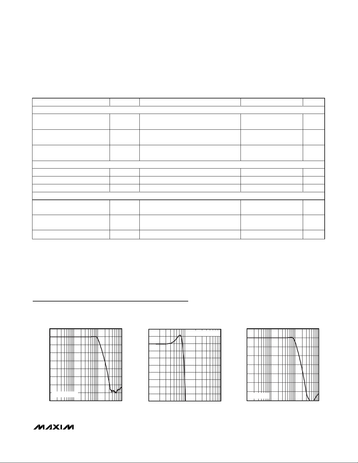
SMALL-SIGNAL GAIN
vs. FREQUENCY
MAX9517/24 toc01
FREQUENCY (Hz)
GAIN (dB)
10M1M
-70
-60
-50
-40
-30
-20
-10
0
10
-80
100k 100M
V
OUT
= 100mV
P-P
SMALL-SIGNAL GAIN FLATNESS
vs. FREQUENCY
MAX9517/24 toc02
FREQUENCY (Hz)
GAIN (dB)
10M
-3.5
-3.0
-2.5
-2.0
-1.5
-1.0
-0.5
0
0.5
1.0
-4.0
1M 100M
V
OUT
= 100mV
P-P
LARGE-SIGNAL GAIN
vs. FREQUENCY
MAX9517/24 toc03
FREQUENCY (Hz)
GAIN (dB)
10M1M
-60
-50
-40
-30
-20
-10
0
10
-70
100k 100M
V
OUT
= 2V
P-P
Typical Operating Characteristics
(VDD= SHDN = 3.3V. Video outputs have RL= 150Ω connected to GND. TA= +25°C, unless otherwise noted.)
PARAMETER SYMBOL CONDITIONS MIN TYP MAX UNITS
CROSSTALK
VIDOUT-to-NO_
VIDIN-to-COM
VIDOUT-to-COM
LOGIC SIGNAL (IN1 AND IN2)
Logic-Low Threshold V
Logic-High Threshold V
Logic-Input Current I
IL
IH
IN
LOGIC SIGNAL (SHDN)
Logic-Low Threshold V
Logic-High Threshold V
Logic-Input Current I
IL
IH
IN
Video circuit is on, f = 20kHz,
VIDOUT = 2V
, RL = 50Ω, CL = 5pF
P-P
Video circuit is shutdown, f = 20kHz,
0.25V
at VIDIN, RL = 600Ω
P-P
Video circuit is on, f = 20kHz,
VIDOUT = 2V
, RL = 50Ω, CL = 5pF
P-P
90 dB
100 dB
90 dB
0.5 V
1.4 V
10 µA
0.3 x
V
DD
0.7 x
V
DD
10 µA
V
V
MAX9517/MAX9524
Standard-Definition Video Filter Amplifiers with
Dual SPST Switches
6 _______________________________________________________________________________________
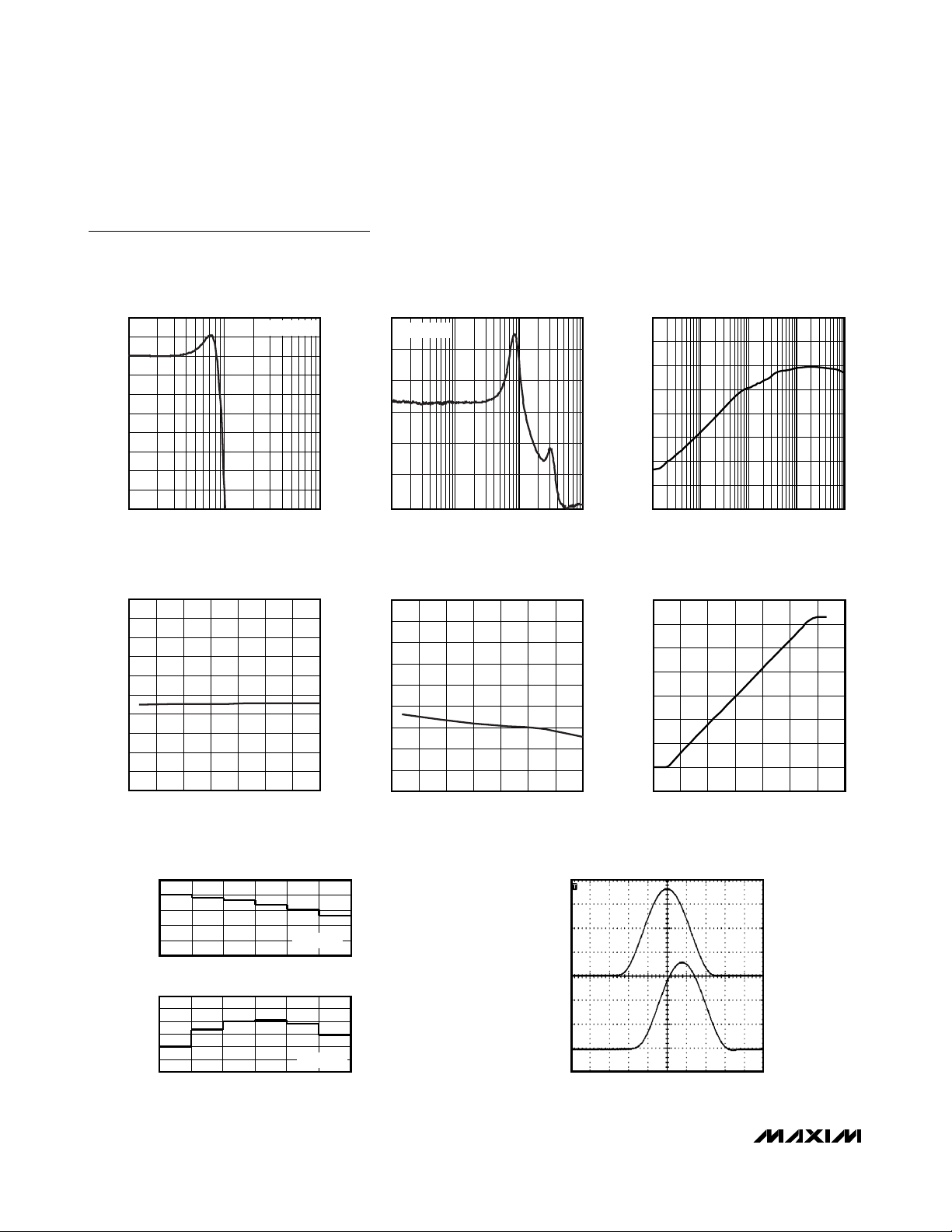
Typical Operating Characteristics (continued)
(VDD= SHDN = 3.3V. Video outputs have RL= 150Ω connected to GND. TA= +25°C, unless otherwise noted.)
LARGE-SIGNAL GAIN FLATNESS
vs. FREQUENCY
MAX9517/24 toc04
FREQUENCY (Hz)
GAIN FLATNESS (dB)
10M
-3.5
-3.0
-2.5
-2.0
-1.5
-1.0
-0.5
0
0.5
1.0
-4.0
1M 100M
V
OUT
= 2V
P-P
GROUP DELAY
vs. FREQUENCY
MAX9517/24 toc05
FREQUENCY (Hz)
GROUP DELAY (ns)
10M1M
20
40
60
80
100
120
0
100k 100M
V
OUT
= 2V
P-P
POWER-SUPPLY REJECTION RATIO
vs. FREQUENCY
MAX9517/24 toc06
FREQUENCY (Hz)
PSRR (dB)
10M1M100k
-70
-60
-50
-40
-30
-20
-10
0
-80
10k 100M
QUIESCENT SUPPLY CURRENT
vs. TEMPERATURE
MAX9517/24 toc07
TEMPERATURE (°C)
QUIESCENT SUPPLY CURRENT (mA)
1007525 500-25
2.5
3.0
3.5
4.0
4.5
5.0
5.5
6.0
6.5
7.0
2.0
-50 125
VOLTAGE GAIN
vs. TEMPERATURE
MAX9517/24 toc08
TEMPERATURE (°C)
VOLTAGE GAIN (V/V)
1007525 500-25
1.96
1.97
1.98
1.99
2.00
2.01
2.02
2.03
2.04
1.95
-50 125
-0.5
0.5
0
1.5
1.0
3.0
2.5
2.0
3.5
-0.3 0.30 0.6 0.9 1.2 1.5 1.8
OUTPUT VOLTAGE
vs. INPUT VOLTAGE (MAX9517)
MAX9517/24 toc09
INPUT VOLTAGE (V)
OUTPUT VOLTAGE (V)
DIFFERENTIAL GAIN AND PHASE
MAX9517/24 toc10
DIFFERENTIAL PHASE (deg)
1324567
1324567
0.6
0.8
0.4
0.2
0
-0.2
-0.4
DIFFERENTIAL GAIN (%)
0
0.1
-0.1
-0.2
-0.3
-0.4
f = 4.43MHz
f = 4.43MHz
100ns/div
2T RESPONSE
VIDIN
200mV/div
VIDOUT
400mV/div
MAX9517/24 toc11
MAX9517/MAX9524
Standard-Definition Video Filter Amplifiers with
Dual SPST Switches
_______________________________________________________________________________________
7
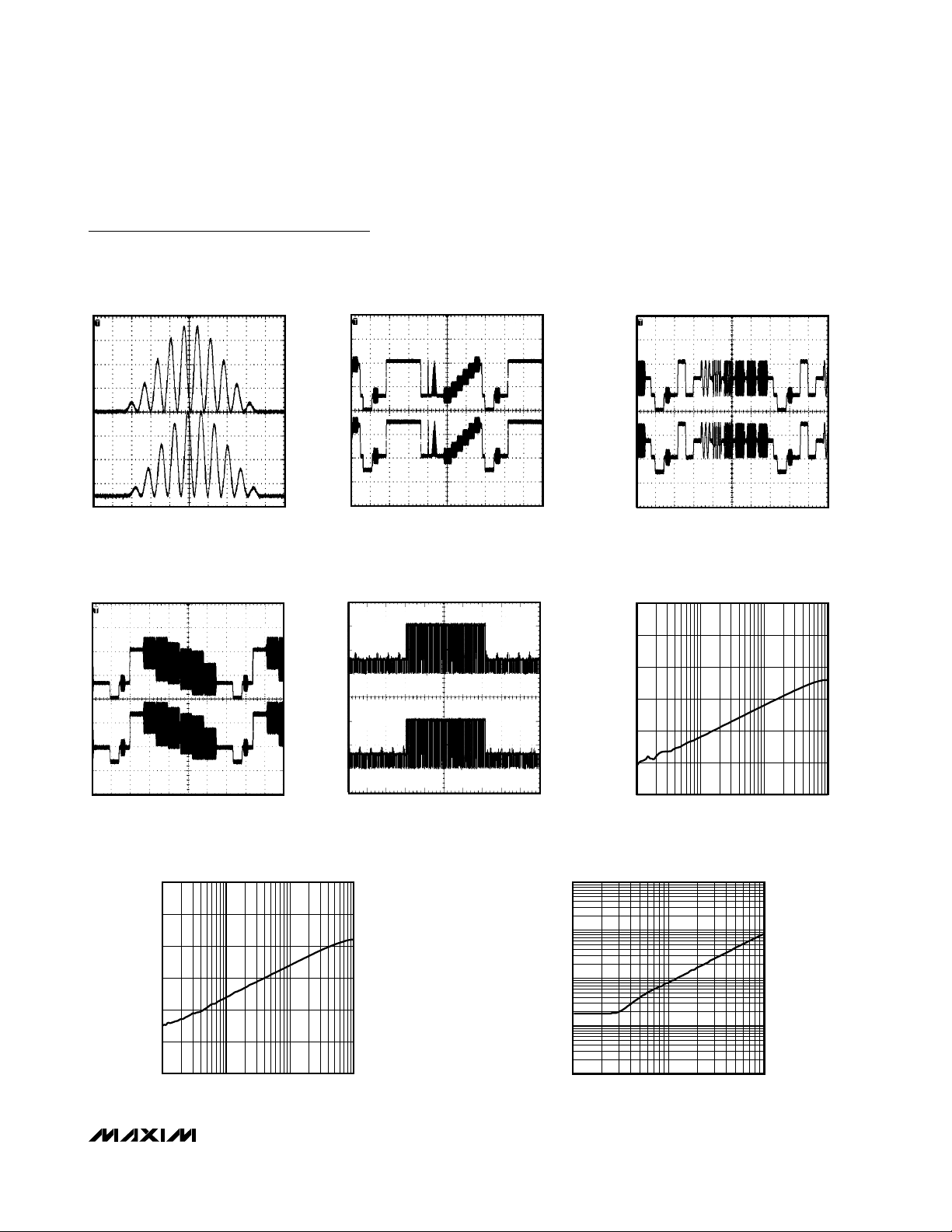
Typical Operating Characteristics (continued)
(VDD= SHDN = 3.3V. Video outputs have RL= 150Ω connected to GND. TA= +25°C, unless otherwise noted.)
SWITCH OUTPUT-TO-OUTPUT CROSSTALK
vs. FREQUENCY
MAX9517/24 toc18
FREQUENCY (Hz)
GAIN (dB)
10M1M
-100
-80
-60
-40
-20
0
-120
100k 100M
OUTPUT IMPEDANCE
vs. FREQUENCY
MAX9517/24 toc19
FREQUENCY (Hz)
OUTPUT IMPEDANCE (Ω)
1M
0.1
1
10
100
0.01
100k 10M
12.5T RESPONSE
400ns/div
PAL COLOR BARS
MAX9517/24 toc12
MAX9517/24 toc15
VIDIN
200mV/div
VIDOUT
400mV/div
VIDIN
500mV/div
VIDOUT
1V/div
NTC-7 VIDEO TEST SIGNAL
10μs/div
FIELD SQUARE-WAVE RESPONSE
MAX9517/24 toc13
MAX9517/24 toc16
VIDIN
500mV/div
VIDOUT
1V/div
VIDIN
500mV/div
VIDOUT
1V/div
PAL MULTIBURST RESPONSE
10μs/div
SWITCH INPUT-TO-INPUT CROSSTALK
vs. FREQUENCY
0
-20
-40
-60
GAIN (dB)
-80
-100
MAX9517/24 toc14
VIDIN
500mV/div
VIDOUT
1V/div
MAX9517/24 toc17
10μs/div
2ms/div
-120
100k 100M
FREQUENCY (Hz)
10M1M
MAX9517/MAX9524
Standard-Definition Video Filter Amplifiers with
Dual SPST Switches
8 _______________________________________________________________________________________8 _______________________________________________________________________________________
Pin Description
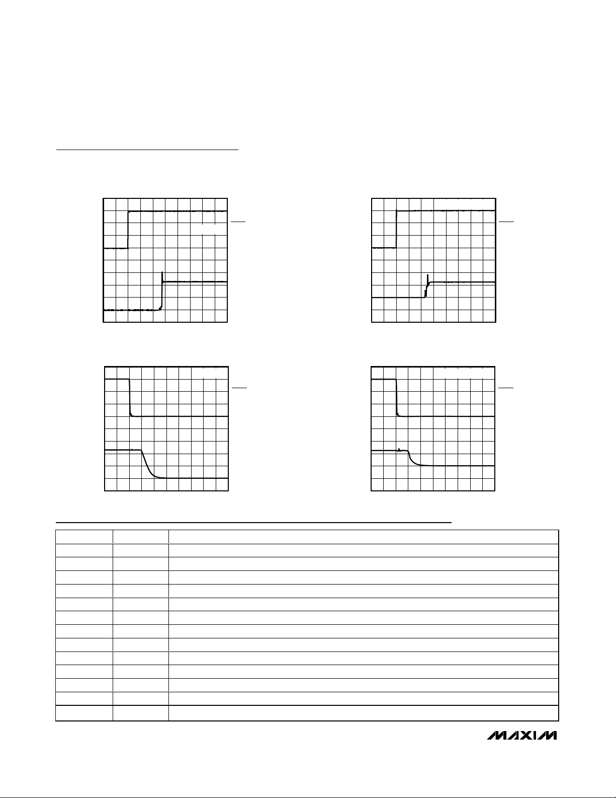
Typical Operating Characteristics (continued)
(VDD= SHDN = 3.3V. Video outputs have RL= 150Ω connected to GND. TA= +25°C, unless otherwise noted.)
MAX9517
DISABLE RESPONSE
MAX9517/24 toc22
10ns/div
OUTPUT
1V/div
SHDN
1V/div
VIN = 1V
MAX9524
DISABLE RESPONSE
MAX9517/24 toc23
10ns/div
OUTPUT
250mV/div
SHDN
1V/div
VIN = 0.1μF TO GND
MAX9517
ENABLE RESPONSE
MAX9517/24 toc20
4ms/div
OUTPUT
1V/div
SHDN
1V/div
VIN = 1V
MAX9524
ENABLE RESPONSE
MAX9517/24 toc21
4ms/div
OUTPUT
250mV/div
SHDN
1V/div
VIN = 0.1μF TO GND
PIN NAME FUNCTION
1 N.C. No Connection. Not internally connected.
2 COM1 Analog Switch 1 Common Terminal
3 COM2 Analog Switch 2 Common Terminal
4 VIDOUT Video Output
5 GND Ground
6 VIDIN Video Input
7 NO2 Analog Switch 2 Normally Open Terminal
8 NO1 Analog Switch 1 Normally Open Terminal
9 SHDN Active-Low Shutdown Input. Connect to GND to place device in shutdown.
10 IN1 Analog Switch 1 Digital Control Input
11 IN2 Analog Switch 2 Digital Control Input
12 V
— EP Exposed Paddle. Connect EP to GND. EP is also internally connected to GND.
DD
Positive Power Supply. Bypass to GND with a 0.1µF capacitor.

MAX9517/MAX9524
Standard-Definition Video Filter Amplifiers with
Dual SPST Switches
_______________________________________________________________________________________ 9
Detailed Description
The MAX9517/MAX9524 consist of a lowpass filter and
an output amplifier capable of driving a standard 150Ω
video load to ground. The MAX9517 has an input buffer
and the MAX9524 has an input sync-tip clamp. The
MAX9517/MAX9524 both have two SPST analog
switches that can be used to route audio, video, or digital signals. The output amplifiers provide a fixed gain of
2V/V.
The MAX9517/MAX9524 filter and amplify the video
DAC output. External video signals, in which the DC
bias is usually not known, can be AC-coupled to the
MAX9524.
Input with DC Buffer (MAX9517)
The input of the MAX9517 can be directly connected to
the video source if the signal is approximately between
ground and 1V. This specification is commonly found at
the output of most video DACs.
DC-coupling requires that the input signals are ground
referenced so that the sync tip of composite or luma
signals is within 50mV of ground.
Input with Sync-Tip Clamp (MAX9524)
When the bias of the incoming video signal is either
unknown or not between ground and 1V (such as an
external video source), use the MAX9524 to connect
the video source through a 0.1µF capacitor.
The VIDIN input of the MAX9524 can only handle signals with a sync pulse, such as composite video and
luma. An internal sync-tip clamp sets the internal DC
level of the video signal.
Video Filter
The filter passband (±1dB) is typically 9MHz to make
the device suitable for standard-definition video signals
from all sources (including broadcast video and DVD).
Broadcast video signals are channel limited: NTSC signals have 4.2MHz bandwidth, and PAL signals have
5MHz bandwidth. Video signals from a DVD player,
however, are not channel limited; therefore, the bandwidth of DVD video signals can approach the Nyquist
limit of 6.75MHz (recommendation ITU-R BT.601-5
specifies 13.5MHz as the sampling rate for standarddefinition video). Therefore, the maximum bandwidth of
the signal is 6.75MHz. To ease the filtering requirements, most modern video systems oversample by two
times, clocking the video current DAC at 27MHz.
Outputs
The video output amplifiers can both source and sink
load current, allowing output loads to be DC- or ACcoupled. The amplifier output stage needs around
300mV of headroom from either supply rail. The parts
have an internal level shift circuit that positions the sync
tip at approximately 300mV at the output.
If the supply voltage is greater than 3.135V (5% below
a 3.3V supply), each amplifier can drive two DC-coupled video loads to ground. If the supply is less than
3.135V, each amplifier can drive only one DC-coupled
or AC-coupled video load.
Shutdown
The MAX9517/MAX9524 draw less than 1µA supply
current when SHDN is low. In shutdown, the amplifier
output becomes high impedance.
Applications Information
Reducing Power Consumption
in the Video DACs
The MAX9517/MAX9524 have high-impedance input
buffers that can work with source resistances as high
as 300Ω. To reduce power dissipation in the video
DACs, the DAC output resistor can be scaled up in
value. The reference resistor that sets the reference
current inside the video DACs must also be similarly
scaled up. For instance, if the output resistor is 37.5Ω,
the DAC must source 26.7mA when the output is 1V. If
the output resistor is increased to 300Ω, the DAC only
needs to source 3.33mA when the output is 1V.
There is parasitic capacitance from the DAC output to
ground. That capacitance in parallel with the DAC output resistor forms a pole that can potentially roll off the
frequency response of the video signal. For example,
300Ω in parallel with 50pF creates a pole at 10.6MHz.
To minimize this capacitance, reduce the area of the
signal trace attached to the DAC output as much as
possible, and place the MAX9517/MAX9524 as close
as possible to the video DAC outputs.
_______________________________________________________________________________________ 9
Table 1. Logic for Analog Switches
SPST Analog Switches
IN_ SWITCH STATE
0 OFF
1ON

MAX9517/MAX9524
Standard-Definition Video Filter Amplifiers with
Dual SPST Switches
10 ______________________________________________________________________________________
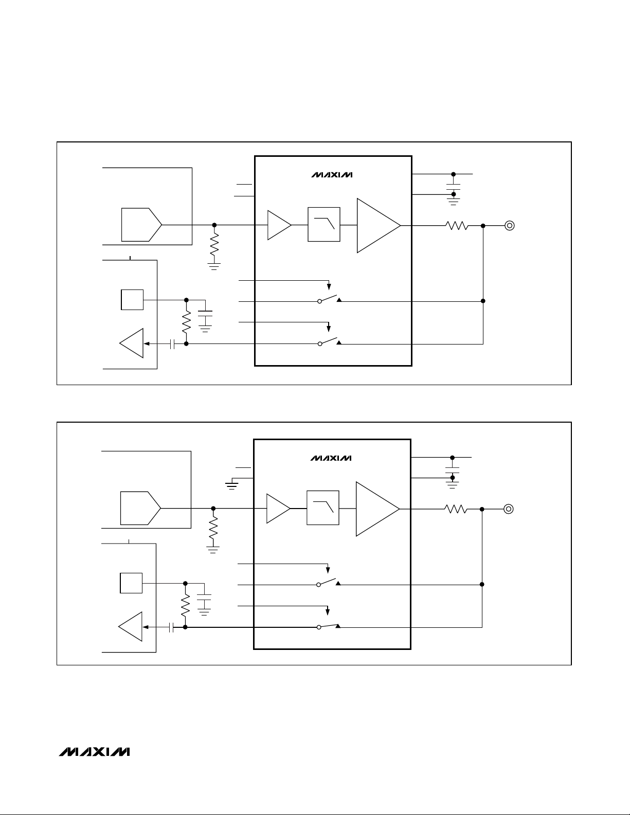
AC-Coupling the Outputs
The outputs can be AC-coupled because the output
stage can source and sink current as shown in Figure 1.
Coupling capacitors should be 220µF or greater to keep
the highpass filter formed by the 150Ω equivalent resistance of the video transmission line to a corner frequency of 4.8Hz or below. The frame rate of PAL systems is
25Hz, and the frame rate of NTSC systems is 30Hz. The
corner frequency should be well below the frame rate.
Changing Between Video Output and
Microphone Input on a Single Connector
A single pole on a mobile phone jack can be used for
transmitting a video signal to a television or receiving
the signal from the microphone of a headset. Figure 2
shows how the MAX9517 can transmit a video signal.
Figure 3 shows how the MAX9517 can receive and
pass on the signal from a microphone.
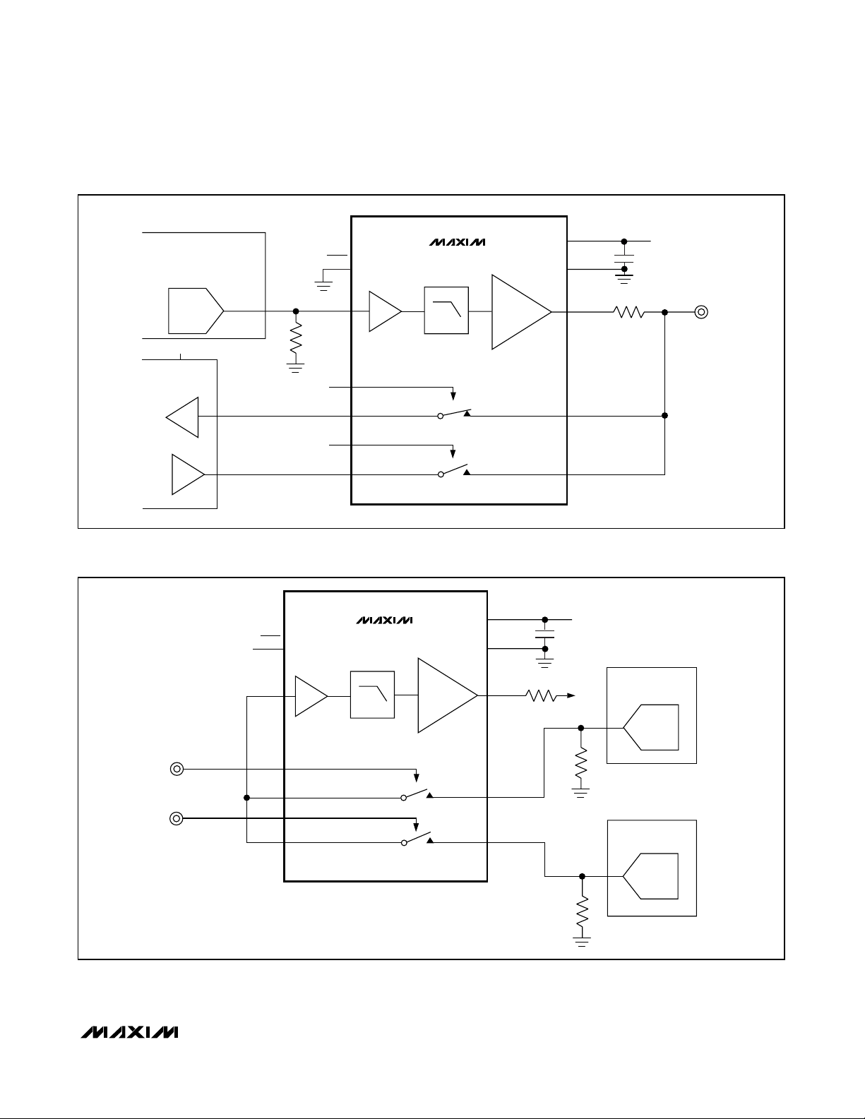
Switching Between Video
and Digital Signals
The dual SPST analog switches and the high-impedance output of the video amplifier enable video transmission, digital transmission, and digital reception all
on a single pole of a connector. Figures 4, 5, and 6
show the different configurations of the MAX9517.
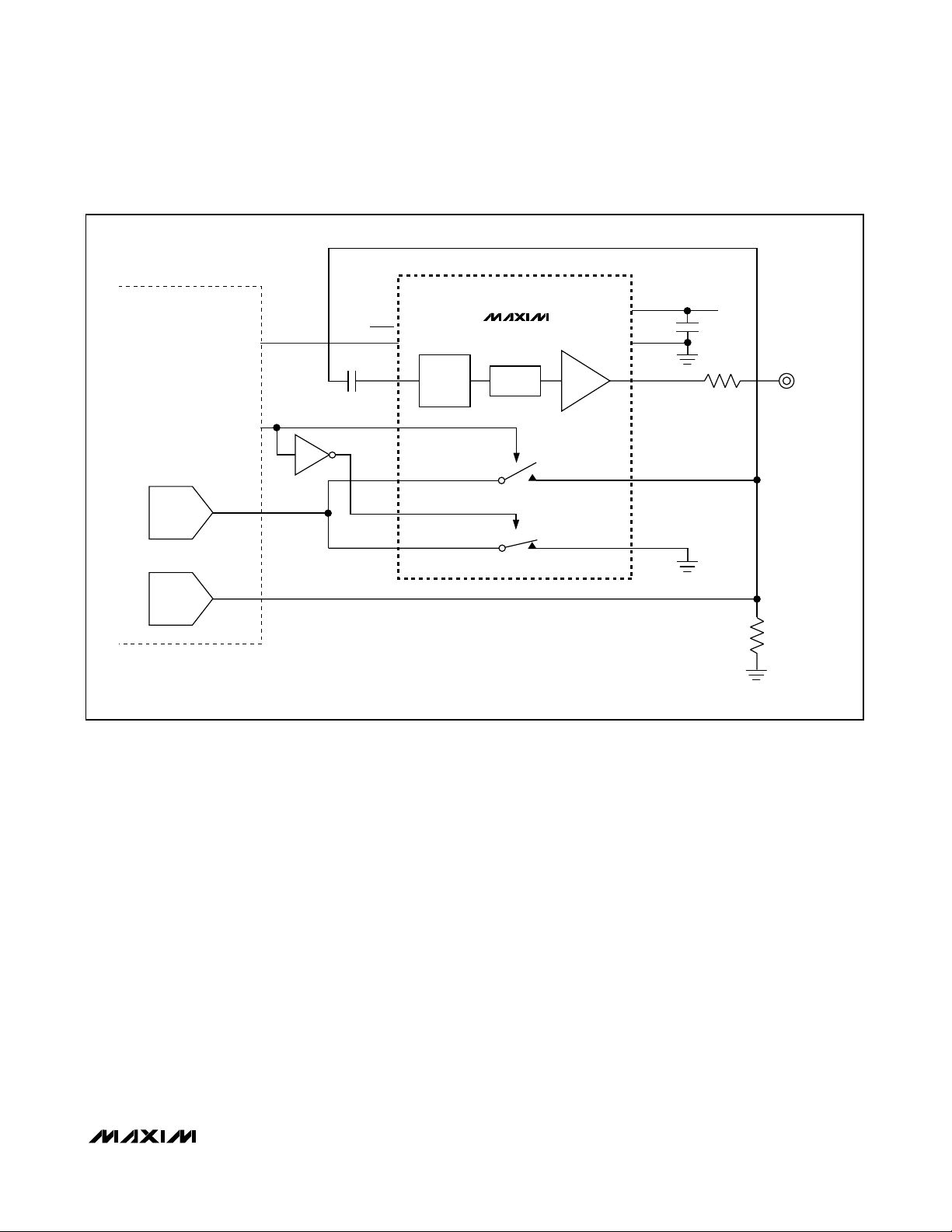
Selecting Between Two Video Sources
The analog switches can multiplex between two video
sources. For example, a mobile phone might have an
application processor with an integrated video encoder
and a mobile graphics processor with an integrated
video encoder, each creating a composite video signal
that is between 0 and 1V. Figure 7 shows this application
in which the MAX9517 chooses between two internal
video sources. The two analog switches can be used as
a 2:1 multiplexer to select which video DAC output is
actually filtered, amplified, and then driven out to the
connector. Close switch 1 to select the video from the
application processor. Close switch 2 to select the video
from the mobile graphics processor.
Figure 8 shows the application in which the MAX9524
chooses between two external video sources with
unknown DC bias.
Y/C Mixer with Chroma Mute
If the video application processor has two current output digital-to-analog converters (DACs) for luma (Y)
and chroma (C), respectively, then the signals can be
mixed together to create a composite video signal by
summing the currents into a single resistor, as shown in
Figure 9. The composite video signal should be ACcoupled into the MAX9524 because the composite
video signal has a positive DC level shift. The sync-tip
clamp of the MAX9524 will re-establish the DC bias
level of the signal inside the chip.
The chroma current is connected to essentially a single-pole, double-throw (SPDT) switch. In one position,
the switch routes the chroma current into the resistor. In
the other position, the switch routes the chroma current
into ground. For the Y/C mixer to work properly, the
chroma current must be routed through analog switch 1
into the resistor.
If the chroma signal needs to be muted, then the chroma
current is shunted to ground through analog switch 2.
Analog switch 1 stays open. See Figure 10.
Figure 1. AC-Coupled Outputs
V
DD
APPLICATION
PROCESSOR
DAC
MICROCONTROLLER
CVBS
SHDN
+3.3V
BUFFER
VIDIN
IN1
NO1
IN2
NO2
MAX9517
LPF
A
V
= 2V/V
GND
VIDOUT
COM1
COM2
+3.3V
0.1μF
75Ω
220μF
CVBS
MAX9517/MAX9524
Standard-Definition Video Filter Amplifiers with
Dual SPST Switches
______________________________________________________________________________________ 11
Figure 2. Video Output Configuration
Figure 3. Microphone Input Configuration
APPLICATION
PROCESSOR
CVBS
DAC
V
CC
V
CC
BASEBAND
IC
MIC
BIAS
OFF
MIC
AMP
OFF
APPLICATION
PROCESSOR
OFF
DAC
CVBS
+3.3V
SHDN
VIDIN
NO1
IN2
NO2
SHDN
VIDIN
IN1
BUFFER
BUFFER
MAX9517
LPF
MAX9517
LPF
A
A
V
= 2V/V
V
= 2V/V
V
DD
GND
VIDOUT
COM1
COM2
V
DD
GND
VIDOUT
+3.3V
0.1μF
75Ω
TO JACK
+3.3V
0.1μF
75Ω
TO JACK
V
CC
V
CC
BASEBAND
IC
MIC
BIAS
MIC
AMP
IN1
NO1
IN2
NO2
OFF
OFF
OFF
COM1
COM2

MAX9517/MAX9524
Standard-Definition Video Filter Amplifiers with
Dual SPST Switches
12 ______________________________________________________________________________________
Figure 4. Video Output Configuration
Figure 5. Digital Output Configuration
APPLICATION
PROCESSOR
CVBS
DAC
V
CC
V
CC
BASEBAND IC
OFF
OFF
+3.3V
SHDN
VIDIN
APPLICATION
PROCESSOR
OFF
DAC
CVBS
SHDN
VIDIN
IN1
NO1
IN2
NO2
BUFFER
BUFFER
MAX9517
LPF
MAX9517
LPF
A
A
V
V
= 2V/V
= 2V/V
V
DD
GND
VIDOUT
COM1
COM2
V
DD
GND
VIDOUT
+3.3V
0.1μF
75Ω
TO JACK
+3.3V
0.1μF
75Ω
TO JACK
V
CC
V
CC
BASEBAND IC
OFF
NO1
IN2
NO2
IN1
OFF
OFF
OFF
COM1
COM2
MAX9517/MAX9524
Standard-Definition Video Filter Amplifiers with
Dual SPST Switches
______________________________________________________________________________________ 13
Figure 6. Digital Input Configuration
Figure 7. Selecting Between Two Internal Video Sources
APPLICATION
PROCESSOR
OFF
DAC
V
CC
V
CC
BASEBAND IC
OFF
CVBS
SHDN
SHDN
VIDIN
NO1
IN2
NO2
IN1
BUFFER
OFF
MAX9517
MAX9517
LPF
OFF
V
DD
GND
A
V
= 2V/V
OFF
+3.3V
0.1μF
V
DD
GND
VIDOUT
COM1
COM2
+3.3V
0.1μF
75Ω
TO JACK
BUFFER
SW1
SW2
VIDIN
IN1
NO1
IN2
NO2
LPF
A
V
= 2V/V
VIDOUT
COM1
COM2
75Ω
APPLICATION
PROCESSOR
DAC
MOBILE
GPU
DAC

MAX9517/MAX9524
Standard-Definition Video Filter Amplifiers with
Dual SPST Switches
14 ______________________________________________________________________________________
Figure 8. Selecting Between Two External Video Sources
Figure 9. Luma and Chroma Mixer Circuit (Chroma Current Routed into Resistor)
SHDN
SW_CONTROL
0.1μF
CVBS_IN1
0.1μF
CVBS_IN2
75Ω75Ω
VIDIN
IN1
NO1
IN2
NO2
MAX9524
LPFCLAMP
6dB
V
DD
GND
VIDOUT
COM1
COM2
+3.3V
0.1μF
75Ω
CVBS_OUT
+3.3V
0.1μF
75Ω
APPLICATION
PROCESSOR
DAC
DAC
C
y
GPIO 1
GPIO 2
0.1μF
SHDN
VIDIN
IN1
NO1
IN2
NO2
MAX9524
LPFCLAMP
6dB
V
DD
GND
VIDOUT
COM1
COM2
CVBS
MAX9517/MAX9524
Standard-Definition Video Filter Amplifiers with
Dual SPST Switches
______________________________________________________________________________________ 15
Figure 10. Luma and Chroma Mixer Circuit with Chroma Muted. Chroma Current is Shunted into Ground Through Analog Switch 2.
+3.3V
0.1μF
75Ω
LUMA
APPLICATION
PROCESSOR
DAC
DAC
GPIO 1
GPIO 2
C
y
0.1μF
SHDN
VIDIN
IN1
NO1
IN2
NO2
MAX9524
LPFCLAMP
6dB
V
DD
GND
VIDOUT
COM1
COM2
MAX9517/MAX9524
Standard-Definition Video Filter Amplifiers with
Dual SPST Switches
16 ______________________________________________________________________________________
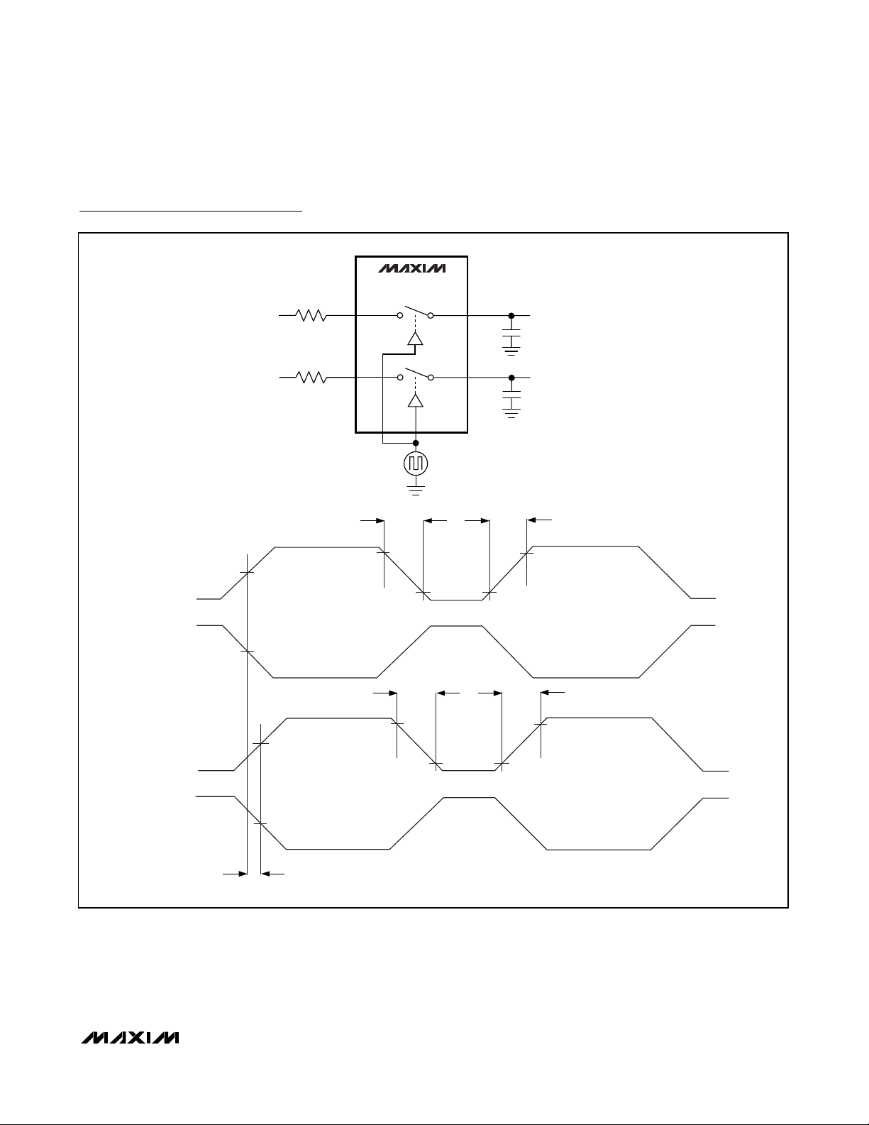
Figure 12. Switching Time
Switch Test Circuits/Timing Diagrams
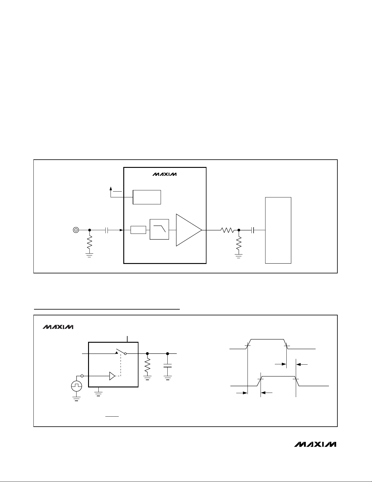
Figure 11. MAX9524 is Used as an Anti-Alias Filter with Buffer (Switches Can Route Other Signals)
Anti-Alias Filter
The MAX9524 can also provide anti-alias filtering with
buffer before an analog-to-digital converter (ADC),
which would be present in an NTSC/PAL video
decoder, for example. Figure 11 shows an example
application circuit for MAX9524. An external composite
video signal is applied to IN, which is terminated with
75Ω to ground. The signal is AC-coupled to VIDIN
because the DC level of an external video signal is usually not well specified.
Power-Supply Bypassing and Ground
The MAX9517/MAX9524 operate from a single-supply
voltage down to 2.7V, allowing for low-power operation.
Bypass V
DD
to GND with a 0.1µF capacitor. Place all
external components as close as possible to the device.
V
DD
SHDN
SHUTDOWN
CIRCUIT
IN
75Ω
0.1μF
VIDIN
CLAMP
MAX9524
LPF
A
= 2V/V
V
VIDOUT
75Ω
75Ω
VIDEO
DECODER
MAX9517
MAX9524
V
NO
IN_
LOGIC
INPUT
GND
INCLUDES FIXTURE AND STRAY CAPACITANCE.
C
L
V
OUT
RL + R
= V
N_ (
R
V
DD
V
DD
COM
R
L
L
)
ON
V
OUT
C
L
SWITCH
OUTPUT
LOGIC
INPUT
V
IH
V
IL
0V
50%
V
OUT
t
ON
0.9 x V
0UT
tr < 5ns
tf < 5ns
t
OFF
0.9 x V
OUT
MAX9517/MAX9524
Standard-Definition Video Filter Amplifiers with
Dual SPST Switches
______________________________________________________________________________________ 17
Figure 13. Output Signal Skew
Switch Test Circuits/Timing Diagrams (continued)
MAX9517
90%
LOGIC
INPUT
MAX9524
t
INFALL
10%
0V TO V
DD
COM1
COM2
t
INRISE
10%
OUT+
C
L
OUT-
C
L
90%
R
S
IN+
IN-
V
DD
V
IN+
0V
50%
NO1
R
S
NO2
V
DD
V
IN-
0V
V
DD
V
OUT+
0V
V
DD
V
OUT-
0V
t
SKEW
50%
50%
50%
90%
t
OUTFALL
10%
V
DD
t
OUTRISE
10%
90%
MAX9517/MAX9524
Standard-Definition Video Filter Amplifiers with
Dual SPST Switches
18 ______________________________________________________________________________________
Figure 14. Charge Injection
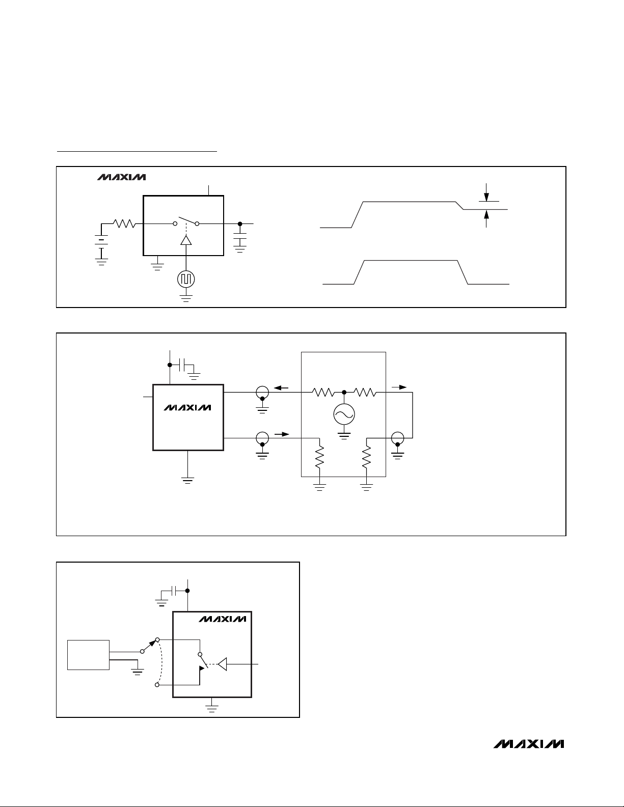
Figure 15. On-Loss, Off-Isolation, and Crosstalk
Figure 16. Channel Off-/On-Capacitance
Switch Test Circuits/Timing Diagrams (continued)
V
IN_
DD
V
DD
COM_
0V TO V
COM_
ΔV
OUT
V
OUT
C
L
DD
V
OUT
ON
IN
NETWORK
V
IN
ANALYZER
50Ω 50Ω
Q = (ΔV
)(CL)
OUT
OFF-ISOLATION = 20log(V
ON-LOSS = 20log(V
CROSSTALK = 20log(V
OFFOFF
OUT/VIN
OUT/VIN
OUT/VIN
)
)
)
MAX9517
MAX9524
R
GEN
+
V
GEN
NO
GND
V
IN_
DD
10nF
V
DD
0V OR V
DD
MAX9517
MAX9524
NO_
GND
MEASUREMENTS ARE STANDARDIZED AGAINST SHORTS AT IC TERMINALS.
OFF-ISOLATION IS MEASURED BETWEEN COM_ AND OFF NO_ TERMINAL ON EACH SWITCH.
ON-LOSS IS MEASURED BETWEEN COM_ AND ON NO_ TERMINAL ON EACH SWITCH.
SIGNAL DIRECTION THROUGH SWITCH IS REVERSED; WORST VALUES ARE RECORDED.
V
DD
10nF
V
DD
MAX9517
MAX9524
GND
CAPACITANCE
ANALYZER
f = 1MHz
COM_
NO_
V
OUT
IN
0V OR V
MEAS REF
50Ω 50Ω
DD

MAX9517/MAX9524
Standard-Definition Video Filter Amplifiers with
Dual SPST Switches
______________________________________________________________________________________ 19
Typical Operating Circuits
APPLICATION
PROCESSOR
DAC
MICROCONTROLLER
CVBS
SHDN
VIDIN
IN1
NO1
IN2
NO2
BUFFER
MAX9517
LPF
+3.3V
0.1μF
75Ω
CVBS
A
= 2V/V
V
V
DD
GND
COM1
COM2
APPLICATION
PROCESSOR
DAC
MICROCONTROLLER
CVBS
V
DD
V
DD
SHDN
0.1μF
VIDIN
CLAMP
IN1
NO1
IN2
NO2
MAX9524
LPF
A
V
= 2V/V
GND
VIDOUT
COM1
COM2
+3.3V
0.1μF
75Ω
CVBS
MAX9517/MAX9524
Standard-Definition Video Filter Amplifiers with
Dual SPST Switches
20 ______________________________________________________________________________________
Pin Configuration
Chip Information
PROCESS: BiCMOS
TOP VIEW
987
10
IN1
11
IN2
12
V
DD
+
12
*EP = EXPOSED PADDLE
(3mm x 3mm)
SHDN
MAX9517
MAX9524
N.C.
THIN QFN
NO1
COM1
EP*
3
NO2
6
5
4
COM2
VIDIN
GND
VIDOUT
MAX9517/MAX9524
Standard-Definition Video Filter Amplifiers with
Dual SPST Switches
______________________________________________________________________________________ 21
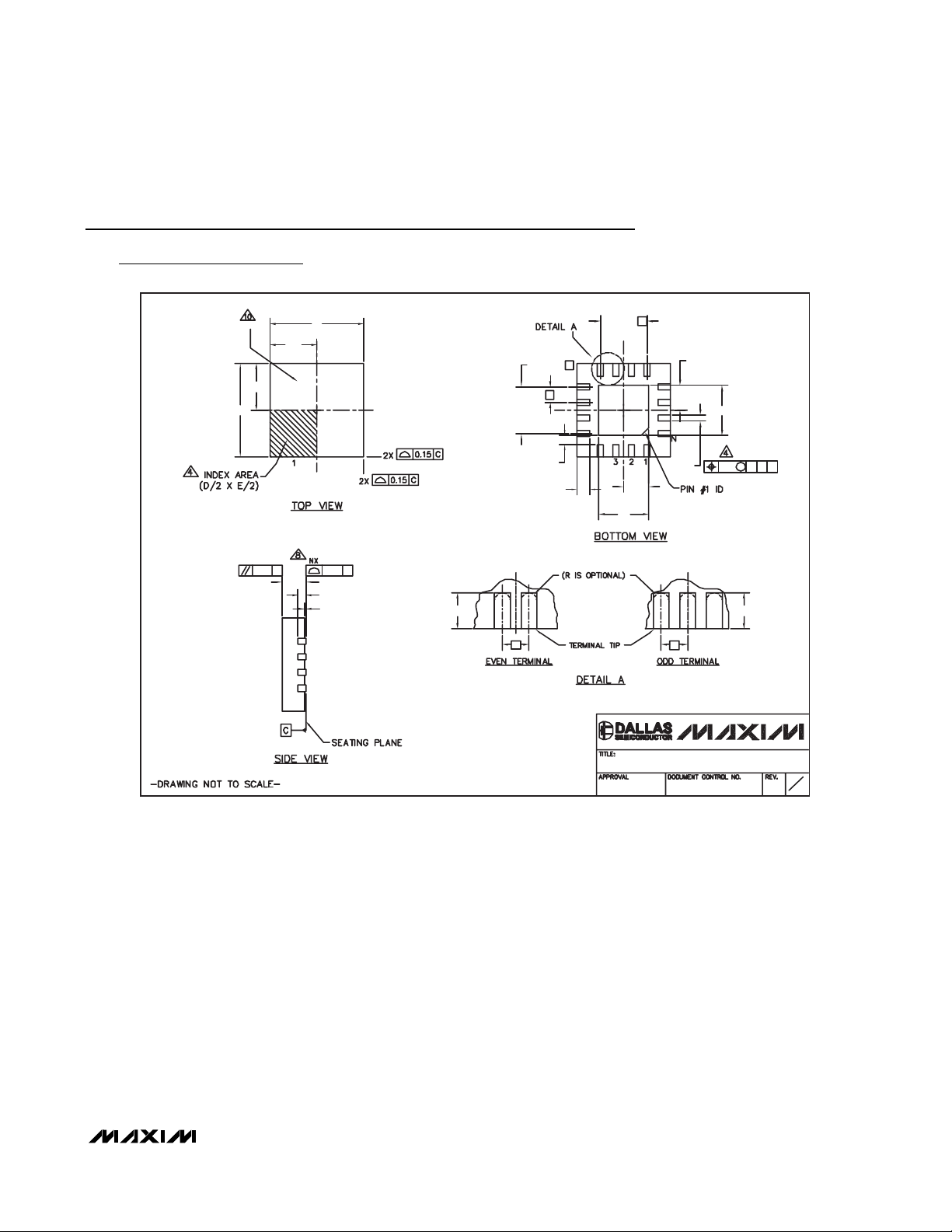
Package Information
(The package drawing(s) in this data sheet may not reflect the most current specifications. For the latest package outline information
go to www.maxim-ic.com/packages
.)
MARKING
D/2
D
E
E/2
AAAA
C
L
0.10 C 0.08 C
A
A2
A1
(NE - 1) X e
(ND - 1) X e
C
L
L
e
k
L
C
L
e
E2/2
E2
D2/2
D2
b
0.10 M C A B
C
L
L
e
12x16L QFN THIN.EPS
PACKAGE OUTLINE
8, 12, 16L THIN QFN, 3x3x0.8mm
21-0136
1
I
2

MAX9517/MAX9524
Standard-Definition Video Filter Amplifiers with
Dual SPST Switches
Maxim cannot assume responsibility for use of any circuitry other than circuitry entirely embodied in a Maxim product. No circuit patent licenses are
implied. Maxim reserves the right to change the circuitry and specifications without notice at any time.
22
____________________Maxim Integrated Products, 120 San Gabriel Drive, Sunnyvale, CA 94086 408-737-7600
© 2007 Maxim Integrated Products is a registered trademark of Maxim Integrated Products, Inc.
Package Information (continued)
(The package drawing(s) in this data sheet may not reflect the most current specifications. For the latest package outline information
go to www.maxim-ic.com/packages
.)
8L 3x3
PKG
REF. MIN.
MIN.
NOM. M
0
3.00 3.10
0.65 BSC.
0.55 0.75
8
2
2
0.02
0.20 REF
-
AX.
0.05
-
0.70 0.75 0.80
A
b
0.25 0.30 0.35
2.90
D
2.90 3.00 3.10
E
e
L
0.35
ND
NE
A1
A2
k
0.25
12L 3x3
NOM. MAX. NOM.
0.70
0.75
0.80
0.20
0.25
0
3.00
3.00
0.50 BSC.
0.55
12N
3
3
0.02
0.20 REF
-
0.30
3.10
3.10
0.65
0.05
-
2.90
2.90
0.45
0.25
16L 3x3
MIN. MAX.
0.70
0.75
0.25
3.00
3.00
0.50 BSC.
0.40
040.02
0.20 REF
0.80
0.30
3.10
3.10
0.50
16
4
0.05
-
0.20
2.90
2.90
0.30
0.25
EXPOSED PAD VARIATIONS
PKG.
CODES
TQ833-1 1.2 50.25 0.70 0.35 x 45° WEEC1.250.700.25
T1233-1
3
T1233-
T1233-4
T1633-2 0.95
T1633F-3
T1633FH-3 0.65 0.80 0.95
T1633-4 0.95
-
T1633-5 0.95
D2
MIN.
0.95
0.95
0.95
0.65
MAX.
NOM.
1.25
1.10
1.25
1.10
1.251.10
1.25
1.10
0.95
0.80
1.10 1.25 0.95 1.10
1.25
1.10
E2
NOM.
MIN.
0.95
0.95 1.10 0.35 x 45°1.25 WEED-1
0.95
0.65
0.65 0.80
MAX.
1.10
1.100.95
1.10
0.80
0.95
1.10
1.25
1.25
0.95
1.25
1.25
ID
PIN
0.35 x 45°
0.35 x 45°
0.35 x 45°
0.225 x 45°
0.225 x 45°
0.35 x 45°
0.35 x 45°
JEDEC
WEED-1
WEED-11.25
WEED-2
WEED-2
WEED-2
WEED-2
WEED-20.95
NOTES:
1. DIMENSIONING & TOLERANCING CONFORM TO ASME Y14.5M-1994.
2. ALL DIMENSIONS ARE IN MILLIMETERS. ANGLES ARE IN DEGREES.
3. N IS THE TOTAL NUMBER OF TERMINALS.
4. THE TERMINAL #1 IDENTIFIER AND TERMINAL NUMBERING CONVENTION SHALL CONFORM TO
JESD 95-1 SPP-012. DETAILS OF TERMINAL #1 IDENTIFIER ARE OPTIONAL, BUT MUST BE LOCATED
WITHIN THE ZONE INDICATED. THE TERMINAL #1 IDENTIFIER MAY BE EITHER A MOLD OR
MARKED FEATURE.
5. DIMENSION b APPLIES TO METALLIZED TERMINAL AND IS MEASURED BETWEEN 0.20 mm AND 0.25 mm
FROM TERMINAL TIP.
6. ND AND NE REFER TO THE NUMBER OF TERMINALS ON EACH D AND E SIDE RESPECTIVELY.
7. DEPOPULATION IS POSSIBLE IN A SYMMETRICAL FASHION.
8. COPLANARITY APPLIES TO THE EXPOSED HEAT SINK SLUG AS WELL AS THE TERMINALS.
9. DRAWING CONFORMS TO JEDEC MO220 REVISION C.
10. MARKING IS FOR PACKAGE ORIENTATION REFERENCE ONLY.
11. NUMBER OF LEADS SHOWN ARE FOR REFERENCE ONLY.
12. WARPAGE NOT TO EXCEED
0.10mm.
PACKAGE OUTLINE
8, 12, 16L THIN QFN, 3x3x0.8mm
21-0136
2
I
2
 Loading...