

General Description
Operating at 1.8V from a single power supply, the
MAX9516 amplifies standard-definition video signals
and only consumes 6mW quiescent power and 12mW
average power. The MAX9516 leverages Maxim’s
DirectDrive™ technology. Combining DirectDrive with
the external positive 1.8V supply, the MAX9516 is able
to drive a 2V
P-P
video signal into a 150Ω load. The
MAX9516 has the ability to detect and report the presence of a video load and reduce power consumption
when the load is not present.
The MAX9516 can detect the presence of a video load
and report a change in load through the LOAD flag.
This feature helps reduce overall system power consumption because the video encoder and the MAX9516
only need to be turned on when a video load is connected. If no load is connected, the MAX9516 is placed
in an active-detect mode and only consumes 31µW.
Maxim’s DirectDrive technology eliminates large outputcoupling capacitors and sets the output video black
level near ground. DirectDrive requires an integrated
charge pump and an internal linear regulator to create
a clean negative power supply so that the amplifier can
pull the sync below ground. The charge pump injects
so little noise into the video output that the picture is
visibly flawless.
The MAX9516 features an internal reconstruction filter
that smoothes the steps and reduces the spikes on the
video signal from the video digital-to-analog converter
(DAC). The reconstruction filter typically has ±1dB
passband flatness of 7.5MHz, and 46dB (typ) attenuation at 27MHz.
The input of the MAX9516 can be directly connected to
the output of a video DAC. The MAX9516 also features
a transparent input sync-tip clamp, allowing AC-coupling of input signals with different DC biases.
The MAX9516 has an internal fixed gain of 8. The input
full-scale video signal is nominally 0.25V
P-P
, and the
output full-scale video signal is nominally 2V
P-P
.
Applications
Digital Still Cameras (DSC)
Digital Video Cameras (DVC)
Mobile Phones
Portable Media Players (PMP)
Security/CCTV Cameras
Automotive Applications
Features
o 1.8V or 2.5V Single-Supply Operation
o Low Power Consumption (6mW Quiescent,
12mW Average)
o Video Load Detect
o Reconstruction Filter with 5.5MHz Passband
o DirectDrive Sets Video Output Black Level Near
Ground
o DC-Coupled Input/Output
o Transparent Input Sync-Tip Clamp
MAX9516
1.8V, Ultra-Low-Power, DirectDrive
Video Filter Amplifier with Load Detect
________________________________________________________________
Maxim Integrated Products
1
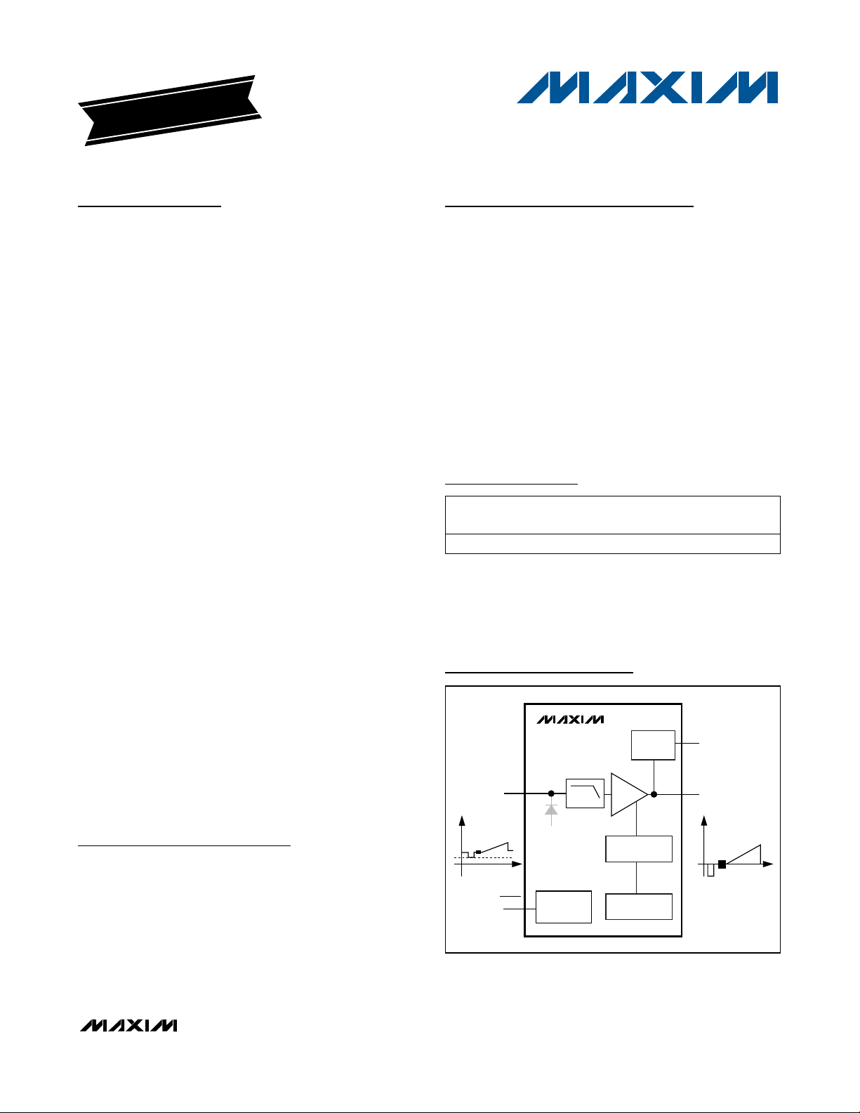
Block Diagram
Ordering Information
0V
2V
P-P
VIDEO
MAX9516
AV =
8V/V
LINEAR
REGULATOR
CHARGE
PUMP
LOAD
SENSE
TRANSPARENT
CLAMP
OUT
LOAD
IN
SHDN
250mV
P-P
VIDEO
LPF
SHUTDOWN
CIRCUIT
19-0995; Rev 0; 9/07
For pricing, delivery, and ordering information, please contact Maxim Direct at 1-888-629-4642,
or visit Maxim’s website at www.maxim-ic.com.
Note: This device operates over the -40°C to +125°C operating
temperature range.
+
Denotes lead-free package.
T = Tape and reel.
Pin Configuration appears at end of data sheet.
EVALUATION KIT
AVAILABLE
PART
PIN-PACKAGE
PKG CODE
TOP
MARK
MAX9516ALB+T
10 µDFN-10 L1022+1
AAN
MAX9516
1.8V, Ultra-Low-Power, DirectDrive
Video Filter Amplifier with Load Detect
2 _______________________________________________________________________________________
ABSOLUTE MAXIMUM RATINGS
ELECTRICAL CHARACTERISTICS
(VDD= SHDN = +1.8V, GND = 0V, OUT has RL= 150Ω connected to GND, C1 = C2 = 1µF, TA= T
MIN
to T
MAX
, unless otherwise
noted. Typical values are at V
DD
= 1.8V, TA= +25°C.) (Note 1)
Stresses beyond those listed under “Absolute Maximum Ratings” may cause permanent damage to the device. These are stress ratings only, and functional
operation of the device at these or any other conditions beyond those indicated in the operational sections of the specifications is not implied. Exposure to
absolute maximum rating conditions for extended periods may affect device reliability.
(Voltages with respect to GND.)
V
DD
...........................................................................-0.3V to +3V
CPGND..................................................................-0.1V to +0.1V
IN................................................................-0.3V to (V
DD
+ 0.3V)
OUT .......................(The greater of V
SS
and -1V) to (VDD+ 0.3V)
SHDN........................................................................-0.3V to +4V
C1P.............................................................-0.3V to (V
DD
+ 0.3V)
C1N .............................................................(V
SS
- 0.3V) to +0.3V
V
SS
............................................................................-3V to +0.3V
Duration of OUT Short Circuit to V
DD
,
GND, and V
SS
.........................................................Continuous
Continuous Current
IN, SHDN, LOAD .............................................................±20mA
Continuous Power Dissipation (T
A
= +70°C)
10-Pin µDFN (derate 5mW/°C above +70°C) ...............403mW
Operating Temperature Range ............................-40°C to +125°C
Junction Temperature........................................................+150°C
Storage Temperature Range .............................-65°C to +150°C
Lead Temperature (soldering, 10s) .................................+300°C
PARAMETER SYMBOL CONDITIONS MIN TYP MAX UNITS
Supply Voltage Range V
Supply Current I
Shutdown Supply Current I
Output Load Detect Threshold RL to GND 200 Ω
Output Level IN = 80mV -85 +9 +85 mV
DC-COUPLED INPUT
Input Voltage Range
Input Current I
Input Resistance R
AC-COUPLED INPUT
Sync-Tip Clamp Level V
Input-Voltage Swing
Sync Crush
Input Clamping Current IN = 130mV 2 3.5 µA
Line Time Distortion CIN = 0.1µF 0.2 %
Minimum Input Source
Resistance
DD
DD
SHDN
CLP
Guaranteed by PSRR 1.700 2.625 V
Amplifier ON,
SHDN = V
SHDN = GND 0.01 10 µA
Guaranteed by
output-voltage
swing
IN = 130mV 2 3.5 µA
B
10mV ≤ IN ≤ 250mV 295 kΩ
IN
CIN = 0.1µF -8 0 +11 mV
Guaranteed by
output-voltage
swing
Percentage reduction in sync pulse at
output, R
DD
SOURCE
Full operation mode,
= 0mV (Note 2)
V
IN
Active-detect mode,
no load
1.7V ≤ VDD ≤ 2.625V 0 262.5
2.375V ≤ V
1.7V ≤ VDD ≤ 2.625V 252.5
2.375V ≤ V
= 37.5Ω, CIN = 0.1µF
≤ 2.625V 0 325
DD
≤ 2.625V 325
DD
3.1 5.3 mA
3µA
1.3 %
25 Ω
mV
mV
P-P
MAX9516
1.8V, Ultra-Low-Power, DirectDrive
Video Filter Amplifier with Load Detect
_______________________________________________________________________________________ 3
ELECTRICAL CHARACTERISTICS (continued)
(VDD= SHDN = +1.8V, GND = 0V, OUT has RL= 150Ω connected to GND, C1 = C2 = 1µF, TA= T
MIN
to T
MAX
, unless otherwise
noted. Typical values are at V
DD
= 1.8V, TA= +25°C.) (Note 1)
PARAMETER SYMBOL CONDITIONS MIN TYP MAX UNITS
DC CHARACTERISTICS
DC Voltage Gain A
Output-Voltage Swing
Power-Supply Rejection Ratio
Shutdown Input Resistance 0V ≤ IN ≤ VDD, SHDN = GND 2.5 MΩ
Output Resistance R
Shutdown Output Resistance 0V ≤ OUT ≤ VDD, SHDN = GND 10.0 MΩ
OUT Leakage Current SHDN = GND 1 µA
Output Short-Circuit Current
AC CHARACTERISTICS
Standard-Definition
Reconstruction Filter
Differential Gain DG
Differential Phase DP
Group-Delay Distortion 100kHz ≤ f ≤ 5MHz, OUT = 2V
Peak Signal to RMS Noise 100kHz ≤ f ≤ 5MHz 64 dB
Power-Supply Rejection Ratio PSRR f = 100kHz, V
2T Pulse-to-Bar K Rating
2T Pulse Response 2T = 200ns 0.3 K%
2T Bar Response
Guaranteed by output-voltage swing
V
(Note 3)
1.7V ≤ VDD ≤
2.625V
2.375V ≤ V
2.625V
1.7V ≤ V
75Ω load resistors
OUT
OUT = 0V, -5mA ≤ I
Sourcing 81
Sinking 45
OUT = 2V
frequency is 100kHz
f = 3.58MHz 1.05
f = 4.43MHz 1.1
f = 3.58MHz 0.4
f = 4.43MHz 0.45
2T = 200ns, bar time is 18µs, the beginning
2.5% and the ending 2.5% of the bar time
is ignored
2T = 200ns, bar time is 18µs, the beginning
2.5% and the ending 2.5% of the bar time
is ignored
0 ≤ VIN ≤ 262.5mV,
DC-coupled input
0 ≤ V
≤ 252.5mV
IN
AC-coupled input
≤
DD
≤ 2.625V, measured between
DD
P-P
0 ≤ V
LOAD
, reference
= 100mV
RIPPLE
≤ 325mV 2.548 2.6 2.652
IN
≤ +5mA 0.02 Ω
±1dB passband
flatness
f = 5.5MHz -0.2
f = 8.5MHz -3.0
f = 27MHz -48.7
P-P
P-P
7.84 8 8.16 V/V
2.058 2.1 2.142
,
P-P
1.979 2.02 2.061
48 58 dB
7.5 MHz
16 ns
54 dB
0.1 K%
0.1 K%
V
P-P
mA
dB
%
Degrees
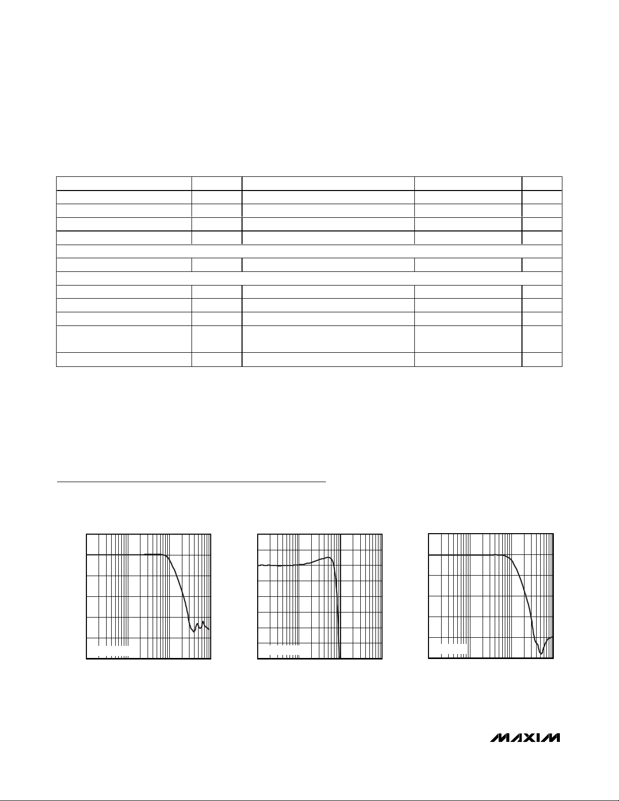
SMALL-SIGNAL GAIN
vs. FREQUENCY
MAX9516 toc01
FREQUENCY (MHz)
GAIN (dB)
101
-80
-60
-40
-20
0
20
-100
0.1 100
V
OUT
= 100mV
P-P
SMALL-SIGNAL GAIN FLATNESS
vs. FREQUENCY
MAX9516 toc02
FREQUENCY (MHz)
GAIN (dB)
101
-2.5
-2.0
-1.5
-1.0
-0.5
0
0.5
1.0
-3.0
0.1 100
V
OUT
= 100mV
P-P
LARGE-SIGNAL GAIN
vs. FREQUENCY
MAX9516 toc03
FREQUENCY (MHz)
GAIN (dB)
101
-80
-60
-40
-20
0
20
-100
0.1 100
V
OUT
= 2V
P-P
Typical Operating Characteristics
(VDD= SHDN = 1.8V, GND = 0V, video output has RL= 150Ω connected to GND, TA= +25°C, unless otherwise noted.)
MAX9516
1.8V, Ultra-Low-Power, DirectDrive
Video Filter Amplifier with Load Detect
4 _______________________________________________________________________________________
ELECTRICAL CHARACTERISTICS (continued)
(VDD= SHDN = +1.8V, GND = 0V, OUT has RL= 150Ω connected to GND, C1 = C2 = 1µF, TA= T
MIN
to T
MAX
, unless otherwise
noted. Typical values are at V
DD
= 1.8V, TA= +25°C.) (Note 1)
Note 1: All devices are 100% production tested at TA= +25°C. Specifications over temperature limits are guaranteed by design.
Note 2: Supply current does not include current supplied to V
OUT
load.
Note 3: Voltage gain (A
V
) is a two-point measurement in which the output-voltage swing is divided by the input-voltage swing.
PARAMETER SYMBOL CONDITIONS MIN TYP MAX UNITS
Nonlinearity 5-step staircase 0.2 %
Output Impedance f = 5MHz, IN = 80mV 7.5 Ω
-to-V
V
OUT
VIN-to-V
CHARGE PUMP
Isolation SHDN = GND, f ≤ 5.5MHz -78 dB
IN
Isolation SHDN = GND, f ≤ 5.5MHz -79 dB
OUT
Switching Frequency 325 625 1150 kHz
LOGIC SIGNALS
Logic-Low Threshold V
Logic-High Threshold V
Logic Input Current IIL, I
Output High Voltage V
Output Low Voltage V
OH
OL
SHDN, VDD = 1.7V to 2.625V 0.5 V
IL
SHDN, VDD = 1.7V to 2.625V 1.4 V
IH
SHDN 10 µA
IH
V
LOAD, IOH = 3mA
DD
0.4
LOAD, IOL = 3mA 0.4 V
V

MAX9516
1.8V, Ultra-Low-Power, DirectDrive
Video Filter Amplifier with Load Detect
_______________________________________________________________________________________
5
Typical Operating Characteristics (continued)
(VDD= SHDN = 1.8V, GND = 0V, video output has RL= 150Ω connected to GND, TA= +25°C, unless otherwise noted.)
LARGE-SIGNAL GAIN FLATNESS
vs. FREQUENCY
1.0
0.5
0
-0.5
-1.0
GAIN (dB)
-1.5
-2.0
-2.5
V
= 2V
OUT
-3.0
0.1 100
P-P
101
FREQUENCY (MHz)
QUIESCENT SUPPLY CURRENT
vs. TEMPERATURE
5.0
4.5
4.0
3.5
3.0
2.5
2.0
QUIESCENT SUPPLY CURRENT (mA)
1.5
1.0
-50 125
TEMPERATURE (°C)
GROUP DELAY
vs. FREQUENCY
110
100
MAX9516 toc04
90
80
70
60
50
DELAY (ns)
40
30
20
10
V
= 2V
OUT
0
0.1 100
P-P
101
FREQUENCY (MHz)
MAX9516 toc05
VOLTAGE GAIN
vs. TEMPERATURE
8.20
8.15
MAX9516 toc07
8.10
8.05
8.00
7.95
VOLTAGE GAIN (V/V)
7.90
7.85
7.80
1007550250-25
-50 125
TEMPERATURE (°C)
MAX9516 toc08
1007550250-25
POWER-SUPPLY REJECTION RATIO
vs. FREQUENCY
20
0
-20
-40
PSSR (dB)
-60
-80
V
= 100mV
RIPPLE
-100
0.1 100
P-P
FREQUENCY (MHz)
OUTPUT VOLTAGE
vs. INPUT VOLTAGE
2.0
1.5
1.0
0.5
0
OUTPUT VOLTAGE (V)
-0.5
-1.0
-1.5
-100 400
INPUT VOLTAGE (mV)
MAX9516 toc06
101
MAX9516 toc09
350300250200150100500-50

MAX9516
1.8V, Ultra-Low-Power, DirectDrive
Video Filter Amplifier with Load Detect
6 _______________________________________________________________________________________
Typical Operating Characteristics (continued)
(VDD= SHDN = 1.8V, GND = 0V, video output has RL= 150Ω connected to GND, TA= +25°C, unless otherwise noted.)
NTC-7 VIDEO TEST SIGNAL
MAX9516 toc13
10µs/div
100mV/div
800mV/div
IN
OUT
0V
0V
FIELD SQUARE-WAVE (AC-COUPLED)
MAX9516 toc14
2ms/div
100mV/div
800mV/div
IN
OUT
0V
0V
DIFFERENTIAL GAIN AND PHASE
1.6
1.2
0.8
0.4
GAIN (%)
DIFFERENTIAL
0
-0.4
1
1.2
0.8
0.4
0
-0.4
PHASE (deg)
DIFFERENTIAL
-0.8
-1.2
1
34567
2
34567
2
MAX9516 toc10
2T RESPONSE
0V
0V
100ns/div
MAX9516 toc11
IN
50mV/div
0V
OUT
400mV/div
0V
12.5T RESPONSE
400ns/div
MAX9516 toc12
IN
50mV/div
OUT
400mV/div

MAX9516
1.8V, Ultra-Low-Power, DirectDrive
Video Filter Amplifier with Load Detect
_______________________________________________________________________________________ 7
Pin Description
Detailed Description
The MAX9516 represents Maxim’s second-generation
of DirectDrive video amplifiers, which meet the requirements of current and future portable equipment:
• 1.8V operation. Engineers want to eliminate the 3.3V
supply in favor of lower supply voltages.
• Lower power consumption. The MAX9516 reduces
average power consumption by up to 75% compared to the 3.3V first-generation devices (MAX9503/
MAX9505).
• Internal fixed gain of 8. As the supply voltages drop
for system chips on deep submicron processes, the
video DAC can no longer create a 1V
P-P
signal at its
output, and the gain of 2 found in the previous generation of video filter amps is not enough.
• Active-detect mode reduces power consumption.
DirectDrive technology is necessary for a voltage-mode
amplifier to output a 2V
P-P
video signal from a 1.8V
supply. The integrated inverting charge pump creates
a negative supply that increases the output range and
gives the video amplifier enough headroom to drive a
2V
P-P
video signal with a 150Ω load.
DirectDrive
Background
Integrated video filter amplifier circuits operate from a
single supply. The positive power supply usually creates video output signals that are level-shifted above
ground to keep the signal within the linear range of the
output amplifier. For applications where the positive DC
level is not acceptable, a series capacitor can be
inserted in the output connection in an attempt to elimi-
nate the positive DC level shift. The series capacitor
cannot truly level-shift a video signal because the average level of the video varies with picture content. The
series capacitor biases the video output signal around
ground, but the actual level of the video signal can vary
significantly depending upon the RC time constant and
the picture content.
The series capacitor creates a highpass filter. Since the
lowest frequency in video is the frame rate, which can be
from 24Hz to 30Hz, the pole of the highpass filter should
ideally be an order of magnitude lower in frequency than
the frame rate. Therefore, the series capacitor must be
very large, typically from 220µF to 3000µF. For spaceconstrained equipment, the series capacitor is unacceptable. Changing from a single-series capacitor to a
SAG network that requires two smaller capacitors only
reduces space and cost slightly.
The series capacitor in the usual output connection
also prevents damage to the output amplifier if the connector is shorted to a supply or to ground. While the
output connection of the MAX9516 does not have a
series capacitor, the MAX9516 will not be damaged if
the connector is shorted to a supply or to ground (see
the
Short-Circuit Protection
section).
Video Amplifier
If the full-scale video signal from a video DAC is
250mV, the black level of the video signal created by
the video DAC is approximately 75mV. The MAX9516
shifts the black level to near ground at the output so
that the active video is above ground and the sync is
below ground. The amplifier needs a negative supply
for its output stage to remain in its linear region when
driving sync below ground.
PIN NAME FUNCTION
1VSSCharge-Pump Negative Power Supply. Bypass with a 1µF capacitor to GND.
2 C1N Charge-Pump Flying Capacitor Negative Terminal. Connect a 1µF capacitor from C1P to C1N.
3 CPGND Charge-Pump Ground
4 C1P Charge-Pump Flying Capacitor Positive Terminal. Connect a 1µF capacitor from C1P to C1N.
5VDDPositive Power Supply. Bypass with a 0.1µF capacitor to GND.
6 LOAD Load-Detect Output. LOAD goes high when an output video load is detected.
7 GND Ground
8 IN Video Input
9 SHDN Active-Low Shutdown. Connect to VDD for normal operation.
10 OUT Video Output

MAX9516
1.8V, Ultra-Low-Power, DirectDrive
Video Filter Amplifier with Load Detect
8 _______________________________________________________________________________________
The MAX9516 has an integrated charge pump and linear regulator to create a low-noise negative supply
from the positive supply voltage. The charge pump
inverts the positive supply to create a raw negative voltage that is then fed into the linear regulator, which filters out the charge-pump noise.
Comparison Between DirectDrive Output
and AC-Coupled Output
The actual level of the video signal varies less with a
DirectDrive output than an AC-coupled output. The
average video signal level can change greatly depending upon the picture content. With an AC-coupled output, the average level will change according to the time
constant formed by the series capacitor and series
resistance (usually 150Ω). For example, Figure 1 shows
an AC-coupled video signal alternating between a
completely black screen and a completely white
screen. Notice the excursion of the video signal as the
screen changes.
With the DirectDrive amplifier, the black level is held at
ground. The video signal is constrained between
-0.3V and +0.7V. Figure 2 shows the video signal from
a DirectDrive amplifier with the same input signal as the
AC-coupled system.
Load Detection
The MAX9516 provides a video load detection feature.
The device enters active-detect mode when it is
enabled (SHDN = VDD). Every 128ms, the part checks
for a load by connecting a 7.5kΩ pullup resistor to the
video output for 1ms. If the video output is pulled up
during the test, then no load is present and LOAD is
low. If the video output stays low during the test, then a
load is connected and LOAD goes high. The state of
LOAD is latched during the sleep time between sense
pulses. All load-detect changes are deglitched over a
nominal 128ms period. The status of the video load
must remain constant during this deglitch period for
LOAD to change state.
If a load is detected, the part enters the full operation
mode and the amplifier, filter, and sync-tip clamp turn
on. The part then continually checks if the load is present by sensing the sinking load current. Therefore, a
black-burst signal (or output signal < 0V) is required to
maintain the detected load status. If the load remains
present, the LOAD pin remains high. If the load is
removed, LOAD goes low and the part goes back to
the active-detect mode in which power consumption is
typically 31µW.
Video Reconstruction Filter
The MAX9516 includes an internal five-pole,
Butterworth lowpass filter to condition the video signal.
The reconstruction filter smoothes the steps and
reduces the spikes created whenever the DAC output
changes value. In the frequency domain, the steps and
spikes cause images of the video signal to appear at
multiples of the sampling clock frequency. The reconstruction filter typically has ±1dB passband flatness of
7.5MHz and 46dB (typ) attenuation at 27MHz.
Transparent Sync-Tip Input Clamp
The MAX9516 contains an integrated, transparent
sync-tip clamp. When using a DC-coupled input, the
sync-tip clamp does not affect the input signal, as long
as it remains above ground. When using an AC-cou-
Figure 1. AC-Coupled Output
Figure 2. DirectDrive Output
2ms/div
0V
INPUT
500mV/div
OUTPUT
500mV/div
INPUT
500mV/div
0V
2ms/div
OUTPUT
1V/div

MAX9516
1.8V, Ultra-Low-Power, DirectDrive
Video Filter Amplifier with Load Detect
_______________________________________________________________________________________ 9
pled input, the sync-tip clamp automatically clamps the
input signal to ground, preventing it from going lower. A
small current of 2µA pulls down on the input to prevent
an AC-coupled signal from drifting outside the input
range of the part.
Using an AC-coupled input will result in some additional variation of the black level at the output. Applying a
voltage above ground to the input pin of the device
always produces the same output voltage, regardless
of whether the input is DC- or AC-coupled. However,
since the sync-tip clamp level (V
CLP
) can vary over a
small range, the video black level at the output of the
device when using an AC-coupled input can vary by an
additional amount equal to the V
CLP
multiplied by the
DC voltage gain (A
V
).
Short-Circuit Protection
In Figure 7, the MAX9516 includes a 75Ω back-termina-
tion resistor that limits short-circuit current if an external
short is applied to the video output. The MAX9516 also
features internal output short-circuit protection to prevent
device damage in prototyping and applications where
the amplifier output can be directly shorted.
Shutdown
The MAX9516 features a low-power shutdown mode for
battery-powered/portable applications. Shutdown
reduces the quiescent current to less than 10nA.
Connecting SHDN to ground (GND) disables the output
and places the MAX9516 into a low-power shutdown
mode. In shutdown mode, the sync-tip clamp, filter,
amplifier, charge pump, and linear regulator are turned
off and the video output is high impedance.
Applications Information
Power Consumption
The quiescent power consumption and average power
consumption of the MAX9516 is remarkably low
because of the 1.8V operation and the DirectDrive
technology. Quiescent power consumption (P
Q
) is the
power consumed by the internal circuitry of the
MAX9516. The formula for calculating PQ is below.
PQ= P
TOTAL
- P
LOAD
P
TOTAL
is the total power drawn from the supply volt-
age, and P
LOAD
is the power consumed by the load
attached to OUT. For the MAX9516, the quiescent
power consumption is typically 6mW.
Average power consumption, which is representative of
the power consumed in a real application, is the total
power drawn from the supply voltage for a MAX9516
driving a 150Ω load to ground with a 50% flat field.
Under such conditions, the average power consumption
for the MAX9516 is 12mW. Table 1 shows the power
consumption with different video signals. The supply
voltage is 1.8V. OUT drives a 150Ω load to ground.
Notice that the two extremes in power consumption
occur with a video signal that is all black and a video
signal that is all white. The power consumption with
75% color bars and a 50% flat field lies in between the
extremes.
Interfacing to Video DACs that Produce
Video Signals Larger than 0.25V
P-P
Devices designed to generate 1V
P-P
video signals at
the output of the video DAC can still work with the
MAX9516. Most video DACs source current into a
ground-referenced resistor, which converts the current
into a voltage. Figure 3 shows a video DAC that creates
a video signal from 0 to 1V across a 150Ω resistor. The
following video filter amplifier has a gain of 2V/V so that
the output is 2V
P-P
.
The MAX9516 expects input signals that are 0.25V
P-P
nominally. The same video DAC can be made to work
with the MAX9516 by scaling down the 150Ω resistor to
a 37.5Ω resistor, as shown in Figure 4. The 37.5Ω resistor is one-quarter of the 150Ω resistor, resulting in a
video signal that is one-quarter the amplitude.
Figure 3. Video DAC generates a 1V
P-P
signal across a 150
Ω
resistor connected to ground.
Table 1. Power Consumption of MAX9516
with Different Video Signals
VIDEO SIGNAL
All Black Screen 6.7
All White Screen 18.2
75% Color Bars 11.6
50% Flat Field 11.7
IMAGE
PROCESSOR
ASIC
DAC
0 TO 1V
150Ω
MAX9516 POWER
CONSUMPTION (mW)
LPF
2V/V
75Ω

MAX9516
1.8V, Ultra-Low-Power, DirectDrive
Video Filter Amplifier with Load Detect
10 ______________________________________________________________________________________
Anti-Alias Filter
The MAX9516 provides anti-alias filtering with buffering
before an analog-to-digital converter (ADC), which is
present in an NTSC/PAL video decoder, for example.
Figure 5 shows an example application circuit. An external composite video signal is applied to VIDIN, which is
terminated with a total of 74Ω (56Ω and 18Ω resistors)
to ground. The signal is attenuated by four, and then
AC-coupled to IN. The normal 1V
P-P
video signal must
be attenuated because with a 1.8V supply, the
MAX9516 can handle only a video signal of approximately 0.25V
P-P
at IN. AC-couple the video signal to IN
because the DC level of an external video signal is usually not well specified, although it is reasonable to
expect that the signal is between -2V and +2V. The 10Ω
series resistor increases the equivalent source resistance to about 25Ω, which is the minimum necessary for
a video source to drive the internal sync-tip clamp.
For external video signals larger than 1V
P-P
, operate
the MAX9516 from a 2.5V supply so that IN can accommodate a 0.325V
P-P
video signal, which is equivalent to
a 1.3V
P-P
video signal at VIDIN.
Figure 4. Video DAC Generates a 0.25V
P-P
Signal Across a
37.5
Ω
Resistor Connected to Ground
Figure 5. MAX9516 Used as an Anti-Alias Filter with Buffer
IMAGE
PROCESSOR
ASIC
DAC
0 TO 0.25V
37.5Ω
MAX9516
LPF
8V/V
75Ω
VIDIN
56Ω
18Ω
10Ω
1.8V
0.1µF
V
DD
0.1µF
SHDN
IN
V
DD
GND CPGND C1P C1N V
SHUTDOWN
CIRCUIT
CLAMP
LPF
DC
LEVEL SHIFT
CHARGE PUMP
C1
1µF
MAX9516
SS
C2
1µF
VIDEO
AMPLIFIER
LINEAR
REGULATOR
LOAD SENSE
LOAD
OUT
75Ω
VIDEO
DECODER
75Ω

MAX9516
1.8V, Ultra-Low-Power, DirectDrive
Video Filter Amplifier with Load Detect
______________________________________________________________________________________ 11
Video Source with a Positive DC Bias
In some applications, the video source generates a signal with a positive DC voltage bias,
i.e.
, the sync tip of
the signal is well above ground. Figure 6 shows an
example in which the outputs of the luma (Y) DAC and
the chroma (C) DAC are connected together. Since the
DACs are current mode, the output currents sum together into the resistor, which converts the resulting current
into a voltage representing a composite video signal.
If the chroma DAC has an independent output resistor
to ground, then the chroma signal, which is a carrier at
3.58MHz for NTSC or at 4.43MHz for PAL, has a positive DC bias to keep the signal above ground at all
times. If the luma DAC has an independent output
resistor to ground, then the luma signal usually does
not have a positive DC bias, and the sync tip is at
approximately ground. When the chroma and luma signals are added together, the resulting composite video
signal still has a positive DC bias. Therefore, the signal
must be AC-coupled into the MAX9516 because the
composite video signal is above the nominal, DC-coupled 0V to 0.25V input range.
Video Signal Routing
Minimize the length of the PCB trace between the output of the video DAC and the input of the MAX9516 to
reduce coupling of external noise into the video signal.
If possible, shield the PCB trace.
Figure 6. Luma (Y) and Chroma (C) Signals Added Together to Create Composite Video Signal (Which is AC-Coupled Into the
MAX9516)
VIDEO
ASIC
DAC
DAC
LUMA (Y)
CHROMA (C)
V
DD
SHDN
IN
0.1µF
CLAMP
MAX9516
LOAD SENSE
LPF
VIDEO
AMPLIFIER
DC
LEVEL SHIFT
LOAD
OUT
75Ω
75Ω
LINEAR
V
1.8V
0.1µF
DD
CHARGE PUMP
GND CPGND C1P C1N V
C1
1µF
REGULATOR
SS
C2
1µF

MAX9516
1.8V, Ultra-Low-Power, DirectDrive
Video Filter Amplifier with Load Detect
12 ______________________________________________________________________________________
Power-Supply Bypassing
and Ground Management
The MAX9516 operates from a 1.7V to 2.625V single
supply and requires proper layout and bypassing. For
the best performance, place the components as close
to the device as possible.
Proper grounding improves performance and prevents
any switching noise from coupling into the video signal.
Bypass the analog supply (VDD) with a 0.1µF capacitor
to GND, placed as close to the device as possible.
Bypass VSSwith a 1µF capacitor to GND as close to
the device as possible. The total system bypass capacitance on V
DD
should be at least 10µF or ten times the
capacitance between C1P and C1N.
Using a Digital Supply
The MAX9516 was designed to operate from noisy digital supplies. The high PSRR (54dB at 100kHz) allows
the MAX9516 to reject the noise from the digital power
supplies (see the
Typical Operating Characteristics
). If
the digital power supply is very noisy and stripes
appear on the television screen, increase the supply
bypass capacitance. An additional, smaller capacitor in
parallel with the main bypass capacitor can reduce
digital supply noise because the smaller capacitor has
lower equivalent series resistance (ESR) and equivalent
series inductance (ESL).
Figure 7. DC-Coupled Input
Typical Operating Circuits
V
DD
SHDN
VIDEO
ASIC
MAX9516
LOAD SENSE
LOAD
DAC
1.8V
0.1µF
IN
TRANSPARENT
V
DD
GND CPGND C1P C1N V
CLAMP
CHARGE PUMP
LPF
DC
LEVEL SHIFT
C1
1µF
SS
C2
1µF
VIDEO
AMPLIFIER
LINEAR
REGULATOR
OUT
75Ω
75Ω

MAX9516
1.8V, Ultra-Low-Power, DirectDrive
Video Filter Amplifier with Load Detect
______________________________________________________________________________________ 13
Figure 8. AC-Coupled Input
Typical Operating Circuits (continued)
Chip Information
PROCESS: BiCMOS
Pin Configuration
123
10
+
98
45
76
OUT IN LOADSHDN
V
SS
V
DD
CPGNDC1N
MAX9516
µDFN
TOP VIEW
GND
C1P
VIDEO
ASIC
DAC
V
DD
SHDN
V
DD
IN
0.1µF
CLAMP
V
1.8V
0.1µF
DD
CHARGE PUMP
GND CPGND C1P C1N V
MAX9516
LPF
DC
LEVEL SHIFT
C1
1µF
SS
C2
1µF
VIDEO
AMPLIFIER
LINEAR
REGULATOR
LOAD SENSE
LOAD
OUT

MAX9516
1.8V, Ultra-Low-Power, DirectDrive
Video Filter Amplifier with Load Detect
14 ______________________________________________________________________________________
Package Information
(The package drawing(s) in this data sheet may not reflect the most current specifications. For the latest package outline information
go to www.maxim-ic.com/packages
.)
XXXX
XXXX
XXXX
D
PIN 1
INDEX AREA
SAMPLE
MARKING
7
A1
A
E
L
b
A
A2
L
e
C
L
e
EVEN TERMINAL
A A
(N/2 -1) x e)
b
N
1
C
L
e
ODD TERMINAL
SOLDER
MASK
COVERAGE
PIN 1
0.10x45∞
L1
6, 8, 10L UDFN.EPS
L
PACKAGE OUTLINE,
6, 8, 10L uDFN, 2x2x0.80 mm
-DRAWING NOT TO SCALE-
21-0164
1
A
2

MAX9516
1.8V, Ultra-Low-Power, DirectDrive
Video Filter Amplifier with Load Detect
Maxim cannot assume responsibility for use of any circuitry other than circuitry entirely embodied in a Maxim product. No circuit patent licenses are
implied. Maxim reserves the right to change the circuitry and specifications without notice at any time.
Maxim Integrated Products, 120 San Gabriel Drive, Sunnyvale, CA 94086 408-737-7600 ____________________
15
© 2007 Maxim Integrated Products is a registered trademark of Maxim Integrated Products, Inc.
Package Information (continued)
(The package drawing(s) in this data sheet may not reflect the most current specifications. For the latest package outline information
go to www.maxim-ic.com/packages
.)
COMMON DIMENSIONS
SYMBOL MIN. NOM.
A
A1
A2
D 1.95 2.00
E
L
L1
PACKAGE VARIATIONS
PKG. CODE N e b
0.70 0.75
0.15 0.20 0.25
0.020 0.025 0.035
1.95 2.00
0.30 0.40
MAX.
0.80
2.05
-
2.05
0.50
0.10 REF.
6L622-1 0.65 BSC 0.30±0.05
0.25±0.050.50 BSC8L822-1
0.20±0.030.40 BSC10L1022-1
(N/2 -1) x e
1.30 REF.
1.50 REF.
1.60 REF.
PACKAGE OUTLINE,
6, 8, 10L uDFN, 2x2x0.80 mm
-DRAWING NOT TO SCALE-
21-0164
2
A
2
 Loading...