

General Description
Operating from a 1.8V single power supply, the MAX9509/
MAX9510 amplify standard-definition video signals and
only consume 5.8mW quiescent power and 11.7mW
average power. The MAX9509/MAX9510 leverage
Maxim’s DirectDrive™ technology to generate a clean,
internal negative supply. Combining the internal negative power supply with the external positive 1.8V supply, the MAX9509/MAX9510 are able to drive a 2V
P-P
video signal into a 150Ω load.
Besides increasing the output voltage range, Maxim’s
DirectDrive technology eliminates large output-coupling
capacitors and sets the output video black level near
ground. DirectDrive requires an integrated charge pump
and an internal linear regulator to create a clean negative
power supply so that the amplifier can pull the sync
below ground. The charge pump injects little noise into
the video output, making the picture visibly flawless.
The MAX9509/MAX9510 are designed to operate from the
1.8V digital power supply. The high power-supply rejection ratio (49dB at 100kHz) allows the MAX9509/
MAX9510 to reject the noise from the digital power supply.
The MAX9509 features an internal reconstruction filter
that smoothes the steps and reduces the spikes on the
video signal from the video digital-to-analog converter
(DAC). The reconstruction filter typically has ±1dB
passband flatness of 8.1MHz and 46dB attenuation at
27MHz. The large-signal, ±1dB passband flatness of
the MAX9510 video amplifier is typically 8.4MHz, and
the large signal -3dB frequency is typically 11.4MHz.
The input of the MAX9509/MAX9510 can be directly
connected to the output of a video DAC. The MAX9509/
MAX9510 also feature a transparent input sync-tip
clamp, allowing AC-coupling of input signals with different DC biases. The MAX9509/MAX9510 have an internal fixed gain of 8. The input full-scale video signal is
nominally 0.25V
P-P
, and the output full-scale video sig-
nal is nominally 2V
P-P
. The devices operate from a 1.8V
or 2.5V single supply and feature a 10nA low-power
shutdown mode. The MAX9509 is offered in an 8-pin
TDFN package and the MAX9510 is offered in an 8-pin
µMAX®package.
Features
o 5.8mW Quiescent Power Consumption
o 11.7mW Average Power Consumption
o 1.8V or 2.5V Single-Supply Operation
o Reconstruction Filter with 8.1MHz Passband and
46dB Attenuation at 27MHz (MAX9509)
o DirectDrive Sets Video Output Black Level near
Ground
o DC-Coupled Input/Output
o Transparent Input Sync-Tip Clamp
o Internal Fixed Gain of 8
o 10nA Shutdown Supply Current
MAX9509/MAX9510
1.8V, Ultra-Low Power, DirectDrive
Video Filter Amplifiers
________________________________________________________________
Maxim Integrated Products
1
Block Diagram
Ordering Information
PART RECONSTRUCTION FILTER PIN-PACKAGE TOP MARK
PACKAGE CODE
MAX9509ATA+T Yes 8 TDFN-EP* AAZ T822-1
MAX9510AUA+T No 8 µMAX-8 — U8-1
19-0727; Rev 1; 4/07
For pricing, delivery, and ordering information, please contact Maxim/Dallas Direct! at
1-888-629-4642, or visit Maxim’s website at www.maxim-ic.com.
Pin Configurations appear at end of data sheet.
Note: All devices are specified over the -40°C to +125°C operating temperature range.
+
Denotes lead-free package.
*
EP = Exposed pad.
µMAX is a registered trademark of Maxim Integrated Products, Inc.
EVALUATION KIT
AVAILABLE
Digital Still Cameras
(DSC)
Digital Video Cameras
(DVC)
Portable Media Players
(PMP)
Mobile Phones
Security/CCTV
Cameras
Automotive
Applications
Applications
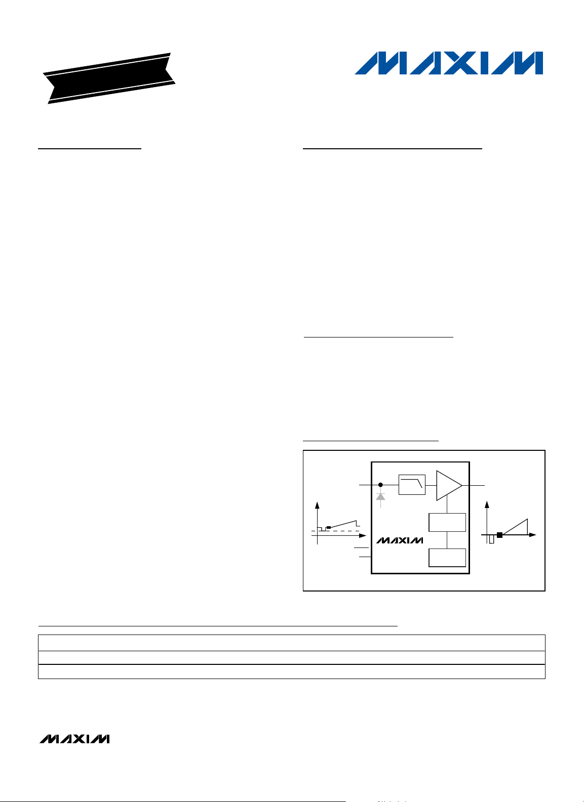
IN
VIDEO
250mV
P-P
SHDN
*FOR MAX9509
LPF*
TRANSPARENT
CLAMP
MAX9509
MAX9510
AV =
8V/V
LINEAR
REGULATOR
CHARGE
PUMP
OUT
0V
VIDEO
2V
P-P
MAX9509/MAX9510
1.8V, Ultra-Low Power, DirectDrive
Video Filter Amplifiers
2 _______________________________________________________________________________________
ABSOLUTE MAXIMUM RATINGS
ELECTRICAL CHARACTERISTICS
(VDD= SHDN = 1.8V, GND = 0V, OUT has RL= 150Ω connected to GND, C1 = C2 = 1µF, TA = T
MIN
to T
MAX
, unless otherwise
noted. Typical values are at T
A
= +25°C.) (Note 1)
Stresses beyond those listed under “Absolute Maximum Ratings” may cause permanent damage to the device. These are stress ratings only, and functional
operation of the device at these or any other conditions beyond those indicated in the operational sections of the specifications is not implied. Exposure to
absolute maximum rating conditions for extended periods may affect device reliability.
(Voltages with respect to GND.)
V
DD
..........................................................................-0.3V to +3V
IN................................................................-0.3V to (V
DD
+ 0.3V)
OUT .......................(The greater of V
SS
and -1V) to (VDD+ 0.3V)
SHDN........................................................................-0.3V to +4V
C1P ............................................................-0.3V to (V
DD
+ 0.3V)
C1N ............................................................(V
SS
- 0.3V) to +0.3V
V
SS
...........................................................................-3V to +0.3V
Duration of OUT Short Circuit to V
DD
,
GND, and V
SS
.........................................................Continuous
Continuous Current
IN, SHDN .......................................................................±20mA
Continuous Power Dissipation (T
A
= +70°C)
8-Pin TDFN (derate 11.9mW/°C above +70°C) .........953.5mW
8-Pin µMAX (derate 4.5mW/°C above +70°C) ..............362mW
Operating Temperature Range ........................-40°C to +125°C
Junction Temperature .....................................................+150°C
Storage Temperature Range .............................-65°C to +150°C
Lead Temperature (soldering, 10s) .................................+300°C
PARAMETER SYMBOL CONDITIONS MIN TYP MAX UNITS
Supply Voltage Range V
Supply Current I
Shutdown Supply Current I
Output Level IN = 80mV -75 +5 +75 mV
DC-COUPLED INPUT
Input Voltage Range
Input Current I
Input Resistance R
AC-COUPLED INPUT
Sync-Tip Clamp Level V
Input-Voltage Swing
Sync Crush
Input Clamping Current IN = 130mV 2 3.2 µA
Line Time Distortion CIN = 0.1µF 0.2 %
Minimum Input Source
Resistance
DD
DD
SHDN
B
IN
CLP
Guaranteed by PSRR 1.700 2.625 V
No load
SHDN = GND 0.01 10 µA
Guaranteed by output
voltage swing
IN = 130mV 2 3.2 µA
10mV ≤ IN ≤ 250mV 280 kΩ
CIN = 0.1µF -8 0 +11 mV
Guaranteed by output
voltage swing
Percentage reduction in sync pulse at output,
R
= 37.5Ω, CIN = 0.1µF
SOURCE
MAX9509 3.1 5.3
MAX9510 2.9 4.9
1.7V ≤ VDD ≤ 2.625V 0 262.5
2.375V ≤ V
1.7V ≤ VDD ≤ 2.625V 252.5
2.375V ≤ V
≤ 2.625V 0 325
DD
≤ 2.625V 325
DD
1.6 %
25 Ω
mV
mA
mV
P-P
MAX9509/MAX9510
1.8V, Ultra-Low Power, DirectDrive
Video Filter Amplifiers
_______________________________________________________________________________________ 3
ELECTRICAL CHARACTERISTICS (continued)
(VDD= SHDN = 1.8V, GND = 0V, OUT has RL= 150Ω connected to GND, C1 = C2 = 1µF, TA = T
MIN
to T
MAX
, unless otherwise
noted. Typical values are at T
A
= +25°C.) (Note 1)
PARAMETER SYMBOL CONDITIONS MIN TYP MAX UNITS
DC CHARACTERISTICS
DC Voltage Gain A
Output Voltage Swing
Power-Supply Rejection
Ratio
Shutdown Input
Resistance
Output Resistance R
Shutdown Output
Resistance
OUT Leakage Current SHDN = GND 1 µA
Output Short-Circuit
Current
AC CHARACTERISTICS (MAX9509)
Standard-Definition
Reconstruction Filter
Differential Gain DG
Differential Phase DP
Group-Delay Distortion 100kHz ≤ f ≤ 5MHz, OUT = 2V
Peak Signal to RMS Noise 100kHz ≤ f ≤ 5MHz 64 dB
Power-Supply Rejection
Ratio
2T Pulse-to-Bar K Rating
2T Pulse Response 2T = 200ns 0.3 K%
2T Bar Response
Nonlinearity 5-step staircase 0.2 %
Output Impedance f = 5MHz, IN = 80mV 6.4 Ω
V
PSRR
OUT
PSRR f = 100kHz, 100mV
Guaranteed by output voltage swing (Note 2) 7.84 7.95 8.16 V/V
1.7V ≤ VDD ≤ 2.625V
2.375V ≤ V
1.7V ≤ V
load resistors
0V ≤ IN ≤ V
OUT = 0V, -5mA ≤ I
0V ≤ OUT ≤ V
Sourcing 82
Sinking 32
OUT
reference frequency
is 100kHz
f = 3.58MHz 1.04
f = 4.43MHz 1.16
f = 3.58MHz 0.54
f = 4.43MHz 0.52
2T = 200ns, bar time is 18µs, the beginning 2.5%
and the ending 2.5% of the bar time are ignored
2T = 200ns, bar time is 18µs, the beginning 2.5%
and the ending 2.5% of the bar time are ignored
= 2V
DD
0V ≤ VIN ≤ 262.5mV,
DC-coupled input
0V ≤ V
AC-coupled input
≤ 2.625V 0V ≤ VIN ≤ 325mV 2.548 2.6 2.652
DD
≤ 2.625V, measured between 75Ω
SHDN = GND 25 MΩ
DD,
≤ +5mA 0.1 Ω
LOAD
SHDN = GND 32 MΩ
DD,
±1dB passband flatness 8.1 MHz
f = 5.5MHz +0.15
f = 10MHz -3
f = 27MHz -46
P-P
P-P
,
≤ 252.5mV
IN
P-P
2.058 2.1 2.142
,
P-P
1.979 2.02 2.061
46 60 dB
14 ns
49 dB
0.1 K%
0.1 K%
Degrees
V
mA
P-P
dB
%
MAX9509/MAX9510
1.8V, Ultra-Low Power, DirectDrive
Video Filter Amplifiers
4 _______________________________________________________________________________________
ELECTRICAL CHARACTERISTICS (continued)
(VDD= SHDN = 1.8V, GND = 0V, OUT has RL= 150Ω connected to GND, C1 = C2 = 1µF, TA = T
MIN
to T
MAX
, unless otherwise
noted. Typical values are at T
A
= +25°C.) (Note 1)
Note 1: All devices are 100% production tested at T
A
= +25°C. Specifications over temperature limits are guaranteed by design.
Note 2: Voltage gain (A
V
) is a two-point measurement in which the output-voltage swing is divided by the input-voltage swing.
PARAMETER SYMBOL CONDITIONS MIN TYP MAX UNITS
OUT-to-IN Isolation SHDN = GND, f ≤ 5.5MHz 102 dB
IN-to-OUT Isolation SHDN = GND, f ≤ 5.5MHz 99 dB
AC CHARACTERISTICS (MAX9510)
Small-Signal -3dB
Bandwidth
Large-Signal -3dB
Bandwidth
Small-Signal 1dB Flatness OUT = 100mV
Large-Signal 1dB Flatness OUT = 2V
Slew Rate OUT = 2V step 43 V/µs
Settling Time to 0.1% OUT = 2V step 124 ns
Differential Gain DG
Differential Phase DP
Group-Delay Distortion 100kHz ≤ f ≤ 5MHz, OUT = 2V
Peak Signal to RMS Noise 100kHz ≤ f ≤ 5MHz 67 dB
Power-Supply Rejection
Ratio
2T Pulse-to-Bar K Rating
2T Pulse Response 2T = 200ns 0.2 K%
2T Bar Response
Nonlinearity 5-step staircase 0.1 %
Output Impedance f = 5MHz, IN = 80mV 7.3 Ω
OUT-to-IN Isolation SHDN = GND, f ≤ 5MHz 98 dB
IN-to-OUT Isolation SHDN = GND, f ≤ 5MHz 94 dB
CHARGE PUMP
Switching Frequency 325 625 1150 kHz
SHDN INPUT
Logic-Low Threshold V
Logic-High Threshold V
Logic Input Current IIL, I
OUT = 100mV
OUT = 2V
f = 3.58MHz 0.70
f = 4.43MHz 0.93
f = 3.58MHz 0.69
f = 4.43MHz 0.83
PSRR f = 100kHz, 100mV
2T = 200ns, bar time is 18µs, the beginning 2.5%
and the ending 2.5% of the bar time are ignored
2T = 200ns, bar time is 18µs, the beginning 2.5%
and the ending 2.5% of the bar time are ignored
IL
IH
VDD = 1.7V to 2.625V 0.5 V
VDD = 1.7V to 2.625V 1.4 V
IH
P-P
P-P
P-P
P-P
P-P
P-P
42.1 MHz
11.4 MHz
36.1 MHz
8.4 MHz
6ns
45 dB
0.2 K%
0.1 K%
10 µA
%
Degrees
MAX9509/MAX9510
1.8V, Ultra-Low Power, DirectDrive
Video Filter Amplifiers
_______________________________________________________________________________________
5
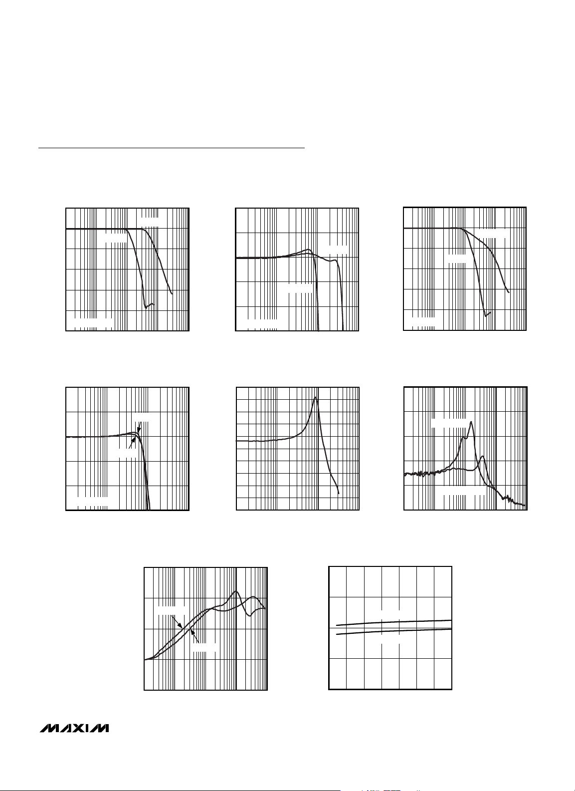
Typical Operating Characteristics
(VDD= SHDN = 1.8V, GND = 0V, DC–coupled input, video output has RL= 150Ω connected to GND, TA= +25°C, unless otherwise
noted.)
POWER-SUPPLY REJECTION RATIO
vs. FREQUENCY
MAX9509/10 toc07
FREQUENCY (Hz)
PSRR (dB)
10M1M100k
-60
-40
-20
0
-80
10k 100M
MAX9510
MAX9509
QUIESCENT SUPPLY CURRENT
vs. TEMPERATURE
MAX9509/10 toc08
TEMPERATURE (°C)
QUIESCENT SUPPLY CURRENT (mA)
1007550250-25
3.5
3.0
2.5
4.0
2.0
-50 125
MAX9509
MAX9510
SMALL-SIGNAL GAIN
vs. FREQUENCY
20
0
-20
-40
GAIN (dB)
-60
-80
V
-100
100k 1G
OUT
= 100mV
MAX9509
P-P
FREQUENCY (Hz)
MAX9510
100M10M1M
LARGE-SIGNAL GAIN FLATNESS
vs. FREQUENCY
2
1
0
GAIN (dB)
-1
-2
V
= 2V
OUT
-3
100k 100M
P-P
MAX9509
MAX9510
10M1M
FREQUENCY (Hz)
MAX9509/10 toc01
MAX9509/10 toc04
SMALL-SIGNAL GAIN FLATNESS
vs. FREQUENCY
2
1
0
GAIN (dB)
-1
-2
V
= 100mV
OUT
-3
100k 100M
MAX9509
P-P
FREQUENCY (Hz)
MAX9510
10M1M
GROUP DELAY vs. FREQUENCY
(MAX9509)
100
90
80
70
60
50
DELAY (ns)
40
30
20
10
0
100k 100M
FREQUENCY (Hz)
10M1M
MAX9509/10 toc02
GAIN (dB)
MAX9509/10 toc05
DELAY (ns)
20
0
-20
-40
-60
-80
-100
100k 1G
40
32
24
16
8
0
100k 1G
LARGE-SIGNAL GAIN
vs. FREQUENCY
MAX9510
MAX9509
V
= 2V
OUT
P-P
100M10M1M
FREQUENCY (Hz)
GROUP DELAY vs. FREQUENCY
(MAX9510)
V
= 2V
OUT
P-P
V
= 100mV
OUT
FREQUENCY (Hz)
P-P
100M10M1M
MAX9509/10 toc03
MAX9509/10 toc06
MAX9509/MAX9510
1.8V, Ultra-Low Power, DirectDrive
Video Filter Amplifiers
6 _______________________________________________________________________________________
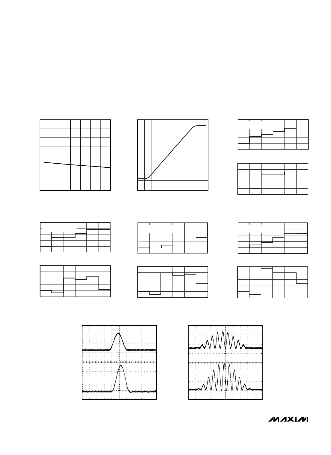
Typical Operating Characteristics (continued)
(VDD= SHDN = 1.8V, GND = 0V, DC–coupled input, video output has RL= 150Ω connected to GND, TA= +25°C, unless otherwise
noted.)
OUTPUT VOLTAGE
vs. INPUT VOLTAGE
MAX9509/10 toc10
INPUT VOLTAGE (mV)
OUTPUT VOLTAGE (V)
350300250200150100500-50
-1.0
-0.5
0
0.5
1.0
1.5
2.0
-1.5
-100 400
DIFFERENTIAL GAIN AND PHASE
(MAX9509)
MAX9509/10 toc11
DC INPUT LEVEL (mV)
DIFFERENTIAL
GAIN (%)
DIFFERENTIAL
PHASE (DEG)
200 232168136
104
0.2
0
0.6
0.4
0.8
-0.4
0
0.8
0.4
1.2
1.6
-0.2
71
DC INPUT LEVEL (mV)
200 232168136
104
71
FREQUENCY = 3.58MHz
IN = 71mV
P-P
DIFFERENTIAL GAIN AND PHASE
(MAX9509)
MAX9509/10 toc12
DC INPUT LEVEL (mV)
DIFFERENTIAL
GAIN (%)
DIFFERENTIAL
PHASE (DEG)
0.2
0
0.6
0.4
0.8
-0.4
0
0.8
0.4
1.2
1.6
-0.2
DC INPUT LEVEL (mV)
FREQUENCY = 4.43MHz
IN = 71mV
P-P
200 232168136
104
71
200 232168136
104
71
DIFFERENTIAL GAIN AND PHASE
(MAX9510)
MAX9509/10 toc13
DC INPUT LEVEL (mV)
DIFFERENTIAL
GAIN (%)
DIFFERENTIAL
PHASE (DEG)
0.2
0
0.6
0.4
0.8
-0.4
0
0.8
0.4
1.2
1.6
-0.2
DC INPUT LEVEL (mV)
FREQUENCY = 3.58MHz
IN = 71mV
P-P
200 232168136
104
71
200 232168136
104
71
DIFFERENTIAL GAIN AND PHASE
(MAX9510)
MAX9509/10 toc14
DC INPUT LEVEL (mV)
DIFFERENTIAL
GAIN (%)
DIFFERENTIAL
PHASE (DEG)
0.2
0
0.6
0.4
0.8
-0.4
0
0.8
0.4
1.2
1.6
-0.2
DC INPUT LEVEL (mV)
FREQUENCY = 4.43MHz
IN = 71mV
P-P
200 232168136
104
71
200 232168136
104
71
2T RESPONSE
MAX9509/10 toc15
200ns/div
IN
100mV/div
0V
0V
OUT
500mV/div
12.5T RESPONSE
MAX9509/10 toc16
400ns/div
IN
100mV/div
0V
0V
OUT
500mV/div
VOLTAGE GAIN
vs. TEMPERATURE
MAX9509/10 toc09
TEMPERATURE (°C)
VOLTAGE GAIN (V/V)
1007550250-25
8.20
7.80
7.85
7.90
7.95
8.00
8.05
8.10
8.15
-50 125

MAX9509/MAX9510
1.8V, Ultra-Low Power, DirectDrive
Video Filter Amplifiers
_______________________________________________________________________________________
7
Typical Operating Characteristics (continued)
(VDD= SHDN = 1.8V, GND = 0V, DC–coupled input, video output has RL= 150Ω connected to GND, TA= +25°C, unless otherwise
noted.)
_______________________________________________________________________________________
7
OUTPUT RESPONSE
TO NTC-7 VIDEO TEST SIGNAL
10µs/div
MAX9509/10 toc17
FIELD SQUARE-WAVE RESPONSE
(AC-COUPLED INPUT)
IN
100mV/div
0V
OUT
500mV/div
0V
PAL MULTIBURST RESPONSE
MAX9509/10 toc20
IN
100mV/div
0V
10µs/div
INPUT
6.25mV/div
MAX9509/10 toc18
IN
100mV/div
0V
OUT
1V/div
0V
SMALL-SIGNAL PULSE RESPONSE
(MAX9510)
PAL COLOR BARS
10µs/div
MAX9509/10 toc21
125mV
MAX9509/10 toc19
IN
100mV/div
0V
OUT
1V/div
0V
INPUT
125mV/div
OUTPUT
1V/div
LARGE-SIGNAL PULSE RESPONSE
(MAX9510)
200ns/div
MAX9509/10 toc22
2ms/div
125mV
360mV
SHDN
1V/div
OUT
250mV/div
V
1V/div
SS
OUT
500mV/div
0V
OUTPUT
50mV/div
ENABLE RESPONSE
100µs/div
MAX9509/10 toc23
IN = 0V
200ns/div
0V
0V
SHDN
1V/div
OUT
250mV/div
V
1V/div
360mV
DISABLE RESPONSE
SS
100µs/div
MAX9509/10 toc24
IN = 0V
0V
0V

MAX9509/MAX9510
1.8V, Ultra-Low Power, DirectDrive
Video Filter Amplifiers
8 _______________________________________________________________________________________8 _______________________________________________________________________________________
Detailed Description
The MAX9509/MAX9510 represent Maxim’s second
generation of DirectDrive video amplifiers that meet the
requirements of current and future portable equipment:
• 1.8V operation. Engineers want to eliminate the 3.3V
supply in favor of lower supply voltages.
• Lower power consumption. The MAX9509/MAX9510
reduce average power consumption by up to 75%
compared to the 3.3V first generation (MAX9503/
MAX9505).
• Internal fixed gain of 8. As the supply voltages drop
for system chips on deep submicron processes, the
video DAC can no longer create a 1V
P-P
signal at its
output, and the gain of 2 found in the previous generation of video filter amplifiers is not enough.
DirectDrive technology is necessary for a voltage mode
amplifier to output a 2V
P-P
video signal from a 1.8V
supply. The integrated inverting charge pump creates
a negative supply that increases the output range and
gives the video amplifier enough headroom to drive a
2V
P-P
video signal with a 150Ω load.
DirectDrive
Background
Integrated video filter amplifier circuits operate from a
single supply. The positive power supply usually creates video output signals that are level-shifted above
ground to keep the signal within the linear range of the
output amplifier. For applications where the positive DC
level is not acceptable, a series capacitor can be
inserted in the output connection in an attempt to eliminate the positive DC level shift. The series capacitor
cannot truly level-shift a video signal because the average level of the video varies with picture content. The
series capacitor biases the video output signal around
ground, but the actual level of the video signal can vary
significantly depending upon the RC time constant and
the picture content.
The series capacitor creates a highpass filter. Since the
lowest frequency in video is the frame rate, which can be
from 24Hz to 30Hz, the pole of the highpass filter should
ideally be an order of magnitude lower in frequency than
the frame rate. Therefore, the series capacitor must be
very large, typically from 220µF to 3000µF. For spaceconstrained equipment, the series capacitor is unacceptable. Changing from a single series capacitor to a
SAG network that requires two smaller capacitors only
reduces space and cost slightly.
The series capacitor in the usual output connection
also prevents damage to the output amplifier if the connector is shorted to a supply or to ground. While the
output connection of the MAX9509/MAX9510 does not
have a series capacitor, the MAX9509/MAX9510 will
not be damaged if the connector is shorted to a supply
or to ground (see the
Short-Circuit Protection
section).
Pin Description
PIN
MAX9509 MAX9510
11VSSCharge-Pump Negative Power Supply. Bypass with a 1µF capacitor to GND.
2 2 C1N
3 3 GND Ground
4 4 C1P
55VDDPositive Power Supply. Bypass with a 0.1µF capacitor to GND.
6 6 IN Video Input
77SHDN Active-Low Shutdown. Connect to VDD for normal operation.
8 8 OUT Video Output
EP — EP Exposed Paddle. EP is internally connected to GND. Connect EP to GND.
NAME FUNCTION
Charge-Pump Flying Capacitor Negative Terminal. Connect a 1µF capacitor from C1P to
C1N.
Charge-Pump Flying Capacitor Positive Terminal. Connect a 1µF capacitor from C1P to
C1N.

Video Amplifier
If the full-scale video signal from a video DAC is 250mV,
the black level of the video signal created by the video
DAC is approximately 75mV. The MAX9509/MAX9510
shift the black level to near ground at the output so that
the active video is above ground and the sync is below
ground. The amplifier needs a negative supply for its output stage to remain in its linear region when driving sync
below ground.
The MAX9509/MAX9510 have an integrated charge
pump and linear regulator to create a low-noise negative supply from the positive supply voltage. The
charge pump inverts the positive supply to create a raw
negative voltage that is then fed into the linear regulator
filtering out the charge-pump noise.
Comparison Between DirectDrive Output
and AC-Coupled Output
The actual level of the video signal varies less with a
DirectDrive output than an AC-coupled output. The
average video signal level can change greatly depending upon the picture content. With an AC-coupled output, the average level will change according to the time
constant formed by the series capacitor and series
resistance (usually 150Ω). For example, Figure 1 shows
an AC-coupled video signal alternating between a
completely black screen and a completely white
screen. Notice the excursion of the video signal as the
screen changes.
With the DirectDrive amplifier, the black level is held at
ground. The video signal is constrained between -0.3V
and +0.7V. Figure 2 shows the video signal from a
DirectDrive amplifier with the same input signal as the
AC-coupled system.
Video Reconstruction Filter (MAX9509)
The MAX9509 includes an internal five-pole, Butterworth
lowpass filter to condition the video signal. The reconstruction filter smoothes the steps and reduces the
spikes created whenever the DAC output changes
value. In the frequency domain, the steps and spikes
cause images of the video signal to appear at multiples
of the sampling clock frequency. The reconstruction filter typically has ±1dB passband flatness of 8.1MHz and
46dB attenuation at 27MHz.
Transparent Sync-Tip Clamp
The MAX9509/MAX9510 contain an integrated, transparent sync-tip clamp. When using a DC-coupled
input, the sync-tip clamp does not affect the input signal, as long as it remains above ground. When using an
AC-coupled input, the transparent sync-tip clamp automatically clamps the input signal to ground, preventing
it from going lower. A small current of 2µA pulls down
on the input to prevent an AC-coupled signal from drifting outside the input range of the part.
Using an AC-coupled input will result in some additional variation of the black level at the output. Applying a
voltage above ground to the input pin of the device
always produces the same output voltage, regardless
of whether the input is DC- or AC-coupled. However,
since the Sync-Tip Clamp Level (V
CLP
) can vary over a
small range, the video black level at the output of the
device when using an AC-coupled input can vary by an
additional amount equal to the V
CLP
multiplied by the
DC Voltage Gain (A
V
).
MAX9509/MAX9510
1.8V, Ultra-Low Power, DirectDrive
Video Filter Amplifiers
_______________________________________________________________________________________ 9
Figure 1. AC-Coupled Output
Figure 2. DirectDrive Output
2ms/div
INPUT
OUTPUT
0V
0V
INPUT
OUTPUT
2ms/div

MAX9509/MAX9510
Short-Circuit Protection
The MAX9509/MAX9510
Functional Diagram/Typical
Application Circuit
includes a 75Ω back-termination
resistor that limits short-circuit current if an external short
is applied to the video output. The MAX9509/MAX9510
also feature internal output short-circuit protection to
prevent device damage in prototyping and applications
where the amplifier output can be directly shorted.
Shutdown
The MAX9509/MAX9510 feature a low-power shutdown
mode for battery-powered/portable applications.
Shutdown reduces the quiescent current to less than
10nA. Connecting SHDN to ground (GND) disables the
output and places the MAX9509/MAX9510 into a lowpower shutdown mode. In shutdown mode, the sync-tip
clamp, filter (MAX9509), amplifier, charge pump, and
linear regulator are turned off and the video output is
high impedance.
Applications Information
Power Consumption
The quiescent power consumption and average power
consumption of the MAX9509/MAX9510 are remarkably
low because of 1.8V operation and DirectDrive technology. Quiescent power consumption is defined when the
MAX9509/MAX9510 are operating without load. In this
case, the MAX9509/MAX9510 consume approximately
5.8mW. Average power consumption, which is defined
when the MAX9509/MAX9510 drive a 150Ω load to
ground with a 50% flat field, is about 11.7mW. Table 1
shows the power consumption with different video signals. The supply voltage is 1.8V. OUT drives a 150Ω
load to ground.
Table 1. Power Consumption of MAX9509/
MAX9510 with Different Video Signals
Notice that the two extremes in power consumption occur
with a video signal that is all black and a video signal that
is all white. The power consumption with 75% color bars
and 50% flat field lies in between the extremes.
Interfacing to Video DACs that Produce
Video Signals Larger than 0.25V
P-P
Devices designed to generate 1V
P-P
video signals at
the output of the video DAC can still work with the
MAX9509/MAX9510. Most video DACs source current
into a ground-referenced resistor, which converts the
current into a voltage. Figure 3 shows a video DAC that
creates a video signal from 0 to 1V across a 150Ω
resistor. The following video filter amplifier has a gain of
2V/V so that the output is 2V
P-P
.
The MAX9509/MAX9510 expect input signals that are
0.25V
P-P
nominally. The same video DAC can be made
to work with the MAX9509/MAX9510 by scaling down the
150Ω resistor to a 37.5Ω resistor, as shown in Figure 4.
The 37.5Ω resistor is 1/4 the size of the 150Ω resistor,
resulting in a video signal that is 1/4 the amplitude.
1.8V, Ultra-Low Power, DirectDrive
Video Filter Amplifiers
10 ______________________________________________________________________________________
Figure 3. The video DAC generates a 1V
P-P
signal across a
150
Ω
resistor connected to ground.
Figure 4. The video DAC generates a 0.25V
P-P
signal across a
37.5
Ω
resistor connected to ground.
VIDEO SIGNAL
All Black Screen 6.7 6.2
All White Screen 18.2 17.9
75% Color Bars 11.6 11.0
50% Flat Field 11.7 11.3
MAX9509 POWER
CONSUMPTION
(mW)
MAX9510 POWER
CONSUMPTION
(mW)
IMAGE
PROCESSOR
ASIC
DAC
IMAGE
PROCESSOR
ASIC
DAC
*FOR MAX9509 ONLY.
0 TO 1V
0 TO 0.25V
150
37.5
LPF
Ω
MAX9509
MAX9510
LPF*
Ω
2V
2V/V
8V/V
P-P
2V
P-P
75
Ω
75
Ω

Anti-Alias Filter
The MAX9509 can also provide anti-alias filtering with a
buffer before an ADC, which would be present in a
NTSC/PAL video decoder, for example. Figure 5 shows
an example application circuit. An external composite
video signal is applied to VIDIN, which is terminated
with a total of 74Ω (56Ω and 18Ω resistors) to ground.
The signal is attenuated by four, and then AC-coupled
to IN. The normal 1V
P-P
video signal must be attenuated because with a 1.8V supply, the MAX9509 can only
handle a video signal of approximately 0.25V
P-P
at IN.
AC-couple the video signal to IN because the DC level
of an external video signal is usually not well specified,
although it is reasonable to expect that the signal is
between -2V and +2V. The 10Ω series resistor increases the equivalent source resistance to approximately
25Ω, which is the minimum necessary for a video
source to drive the internal sync-tip clamp.
For external video signals larger than 1V
P-P
, operate
the MAX9509 from a 2.5V supply so that IN can accommodate a 0.325V
P-P
video signal, which is equivalent to
a 1.3V
P-P
video signal at VIDIN.
MAX9509/MAX9510
1.8V, Ultra-Low Power, DirectDrive
Video Filter Amplifiers
______________________________________________________________________________________ 11
Figure 5. MAX9509 Used as an Anti-Alias Filter with Buffer
V
DD
VIDIN
56Ω
10Ω
18Ω
= 1.8V
V
DD
SHDN
0.1µF
IN
CLAMP
V
DD
MAX9509
SHUTDOWN
CIRCUIT
LPF
CHARGE PUMP
DC-LEVEL
V
DD
AV = 8V/V
SHIFT
LINEAR
REGULATOR
OUT
75Ω
75Ω
VIDEO
DECODER
C3
0.1µF
GND C1P
C1
1µF
C1N
V
SS
C2
1µF

MAX9509/MAX9510
Video Source with a Positive DC Bias
In some applications, the video source generates a signal with a positive DC voltage bias, i.e., the sync tip of
the signal is well above ground. Figure 6 shows an
example in which the outputs of the luma (Y) DAC and
the chroma (C) DAC are connected together. Since the
DACs are current-mode, the output currents sum together into the resistor, which converts the resulting current
into a voltage representing a composite video signal.
If the chroma DAC has an independent output resistor
to ground, then the chroma signal, which is a carrier at
3.58MHz for NTSC or at 4.43MHz for PAL, has a positive DC bias to keep the signal above ground at all
times. If the luma DAC has an independent output
resistor to ground, then the luma signal usually does
not have a positive DC bias, and the sync tip is at
approximately ground. When the chroma and luma signals are added together, the resulting composite video
signal still has a positive DC bias. Therefore, the signal
must be AC-coupled into the MAX9509/MAX9510
because the composite video signal is above the nominal, DC-coupled input range of 0 to 0.25V.
Video Signal Routing
Minimize the length of the PCB trace between the output of the video DAC and the input of the MAX9509/
MAX9510 to reduce coupling of external noise into the
video signal. If possible, shield the PCB trace.
1.8V, Ultra-Low Power, DirectDrive
Video Filter Amplifiers
12 ______________________________________________________________________________________
Figure 6. Luma (Y) and chroma (C) signals are added together to create a composite video signal, which is AC-coupled into the
MAX9509/MAX9510.
V
DD
DD
= 1.8V
SHDN
V
IN
DD
VIDEO
ASIC
DAC
DAC
Y
0.1µF
C
V
MAX9509
MAX9510
V
SHUTDOWN
CIRCUIT
LPF*
CLAMP
DC-LEVEL
SHIFT
CHARGE PUMP
DD
AV = 8V/V
LINEAR
REGULATOR
OUT
75Ω
75Ω
C3
*FOR MAX9509 ONLY.
0.1µF
GND C1P
1µF
C1N
V
SS
C2
C1
1µF

Power-Supply Bypassing and Ground
Management
The MAX9509/MAX9510 operate from a 1.7V to 2.625V
single supply and require proper layout and bypassing.
For the best performance, place the components as
close to the device as possible.
Proper grounding improves performance and prevents
any switching noise from coupling into the video signal.
Bypass the analog supply (V
DD
) with a 0.1µF capacitor
to GND, placed as close to the device as possible.
Bypass V
SS
with a 1µF capacitor to GND as close to
the device as possible. The total system bypass capacitance on V
DD
should be at least 10µF or ten times the
capacitance between C1P and C1N.
Using a Digital Supply
The MAX9509/MAX9510 were designed to operate
from noisy digital supplies. The high PSRR (49dB at
100kHz) allows the MAX9509/MAX9510 to reject the
noise from the digital power supplies (see the
Typical
Operating Characteristics
). If the digital power supply
is very noisy and stripes appear on the television
screen, increase the supply bypass capacitance. An
additional, smaller capacitor in parallel with the main
bypass capacitor can reduce digital supply noise
because the smaller capacitor has lower equivalent
series resistance (ESR) and equivalent series inductance (ESL).
MAX9509/MAX9510
1.8V, Ultra-Low Power, DirectDrive
Video Filter Amplifiers
______________________________________________________________________________________ 13
Functional Diagram/Typical Application Circuit
V
DD
VIDEO
ASIC
SHDN
DC-COUPLED INPUT
MAX9509
MAX9510
SHUTDOWN
CIRCUIT
V
DD
DAC
*FOR MAX9509 ONLY.
IN
LPF*
TRANSPARENT
= 1.8V
V
DD
V
DD
C3
0.1µF
CLAMP
GND C1P
DC-LEVEL
CHARGE PUMP
C1N
C1
1µF
SHIFT
V
SS
C2
1µF
AV = 8V/V
LINEAR
REGULATOR
OUT
75Ω
75Ω

MAX9509/MAX9510
1.8V, Ultra-Low Power, DirectDrive
Video Filter Amplifiers
14 ______________________________________________________________________________________
Pin Configurations
Chip Information
PROCESS: BiCMOS
TOP VIEW
OUT IN V
SHDN
8
7
DD
65
+
V
1
SS
8
OUT
MAX9509
+
134
2
V
SS
*EP = EXPOSED PAD.
TDFN
EP*
GND C1PC1N
C1N
2
MAX9510
GND
3
C1P
4
µMAX
SHDN
7
6
IN
5
V
DD

MAX9509/MAX9510
1.8V, Ultra-Low Power, DirectDrive
Video Filter Amplifiers
______________________________________________________________________________________ 15
Package Information
(The package drawing(s) in this data sheet may not reflect the most current specifications. For the latest package outline information
go to www.maxim-ic.com/packages
.)
8L TDFN EXPOSED PADS.EPS
PACKAGE OUTLINE
6 & 8L TDFN EXPOSED PAD, 2x2x0.80mm
21-0168
1
D
2

MAX9509/MAX9510
1.8V, Ultra-Low Power, DirectDrive
Video Filter Amplifiers
16 ______________________________________________________________________________________
Package Information (continued)
(The package drawing(s) in this data sheet may not reflect the most current specifications. For the latest package outline information
go to www.maxim-ic.com/packages
.)
COMMON DIMENSIONS
SYMBOL
D
E
L
k
MIN.
A
A1
A2
0.70
1.90
0.00
0.20
0.25 MIN.
0.20 REF.
MAX.
0.80
2.101.90
2.10
0.05
0.40
PACKAGE VARIATIONS
PKG. CODE
T622-1
N
6
0.90±0.10
E2D2
1.60±0.10 1.30 REF
1.30±0.10 1.50 REF0.25±0.050.50 TYP. 0.70±0.108T822-1
1.20±0.10 1.50 REF0.25±0.050.50 TYP. 0.80±0.108T822-2 0.125
e
0.65 TYP.
b
0.30±0.05
r
0.150
0.125
[(N/2)-1] x e
PACKAGE OUTLINE
6 & 8L TDFN EXPOSED PAD, 2x2x0.80mm
21-0168
2
D
2

MAX9509/MAX9510
1.8V, Ultra-Low Power, DirectDrive
Video Filter Amplifiers
Maxim cannot assume responsibility for use of any circuitry other than circuitry entirely embodied in a Maxim product. No circuit patent licenses are
implied. Maxim reserves the right to change the circuitry and specifications without notice at any time.
Maxim Integrated Products, 120 San Gabriel Drive, Sunnyvale, CA 94086 408-737-7600 ____________________
17
© 2007 Maxim Integrated Products is a registered trademark of Maxim Integrated Products, Inc.
Springer
Package Information (continued)
(The package drawing(s) in this data sheet may not reflect the most current specifications. For the latest package outline information
go to www.maxim-ic.com/packages
.)
Revision History
Pages changed at Rev 1: 1, 2, 7, 9, 13, 15–17
8
Ø0.50±0.1
0.6±0.1
0.6±0.1
1
D
TOP VIEW
A2
E H
A1
4X S
BOTTOM VIEW
A
8
1
DIM
A
A1
A2
b
c
D
e
E
H
L
α
S
INCHES
MIN
-
0.002
0.030
0.010
0.005
0.116
0.0256 BSC
0.116
0.188
0.016
0°
0.0207 BSC
0.043
0.006
0.037
0.014
0.007
0.120
0.120
0.198
0.026
MAX
6°
MILLIMETERS
MIN
0.05 0.15
0.25 0.36
0.13 0.18
2.95 3.05
2.95 3.05
4.78
0.41
MAX
- 1.10
0.950.75
0.65 BSC
5.03
0.66
0.5250 BSC
6°0°
8LUMAXD.EPS
e
FRONT VIEW
c
b
L
SIDE VIEW
α
PROPRIETARY INFORMATION
TITLE:
PACKAGE OUTLINE, 8L uMAX/uSOP
REV.DOCUMENT CONTROL NO.APPROVAL
21-0036
1
J
1
 Loading...