

General Description
The MAX9508 video filter amplifier with SmartSleep and
bidirectional video support is ideal for set-top boxes
(STBs), portable DVD players, and portable media
players (PMPs). The inputs can be directly connected
to the digital-to-analog converter (DAC) outputs. The
reconstruction filter removes high-frequency signals
above 6.75MHz. The amplifiers have 6dB of gain, and
the outputs can be DC-coupled to a load of 75Ω,
which is equivalent to two video loads, or it can be
AC-coupled to a load of 150Ω.
The SmartSleep circuitry intelligently reduces power
consumption based on the presence of the input signal
and the output loads. When the MAX9508 does not
detect the presence of sync on the input video signal,
the supply current is reduced to less than 7µA. The
device only enables a video amplifier when there is an
active video input signal and an attached load. The
video amplifier remains on while a load is connected. If
the load is disconnected, the video amplifier is turned off.
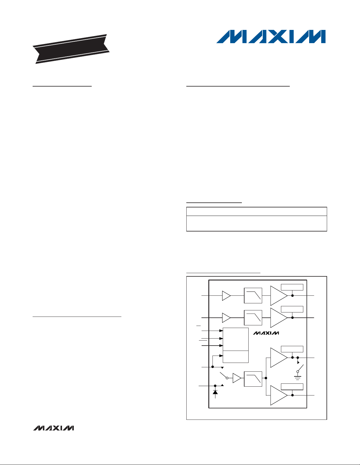
The MAX9508 contains three reconstruction filters, four
video amplifiers, and a pulldown switch at one of the
two CVBS outputs. The MAX9508 has the ability to control the bidirectional video signals at the CVBS video
connections without the need for separate switches or
relays. This feature is particularly useful for portable
DVD players, which often use the same connector to
drive a composite video output and to accept an external video signal to display on the LCD panel.
The MAX9508 operates from a 2.7V to 3.6V single supply
and is offered in a small 16-pin TQFN (3mm x 3mm)
package. The device is specified over the -40°C to
+125°C automotive temperature range.
Applications
Portable DVD Players
Set-Top Boxes (STBs)
Portable Set-Top Boxes/
Personal Video Recorders (PVRs)
Portable Media Players (PMPs)
Portable Applications
Features
♦ SmartSleep Feature Detects Input Signal and
Output Load Status to Reduce Power
Consumption
♦ Triple Standard-Definition Video Reconstruction
Filters with 6.75MHz Passband
♦ Luma, Chroma, and Composite Inputs
♦ Luma, Chroma, and Two Composite Outputs
♦ Integrated Support for a Bidirectional Composite
Video Signal
♦ Supports Two Video Loads at Each Output
(DC-Coupled)
♦ 2.7V to 3.6V Single-Supply Operation
MAX9508
CVBS/S-Video Filter Amplifier with
SmartSleep and Bidirectional Video Support
________________________________________________________________
Maxim Integrated Products
1
Ordering Information
19-0531; Rev 2; 1/09
EVALUATION KIT
AVAILABLE
Block Diagrams
Note: Device is specified over the -40°C to +125°C operating
temperature range.
+
Denotes lead(Pb)-free/RoHS-compliant package.
*
EP = Exposed pad.
Pin Configurations appear at end of data sheet.
Block Diagrams continued at end of data sheet.
For pricing, delivery, and ordering information, please contact Maxim Direct at 1-888-629-4642,
or visit Maxim’s website at www.maxim-ic.com.
PART PIN-PACKAGE TOP MARK
MAX9508ATE+
16 TQFN-EP*
(3mm x 3mm)
AEM
CIN
YIN
INT/EXT
SMARTSLEEP
SHDN
CVBSIN
BUFFER
BUFFER
ACTIVE VIDEO
CONTROL
LOGIC
DETECT
BUFFER
LPF
LPF
MAX9508
6dB
6dB
6dB
LOAD SENSE
COUT
LOAD SENSE
YOUT
LOAD SENSE
CVBSOUT1
LPF
LOAD SENSE
6dB
CVBSOUT2
EXTCVBSIN
CLAMP
MAX9508
CVBS/S-Video Filter Amplifier with
SmartSleep and Bidirectional Video Support
2 _______________________________________________________________________________________
ABSOLUTE MAXIMUM RATINGS
ELECTRICAL CHARACTERISTICS
(VDD= V
SHDN
= 3.3V, V
SMARTSLEEP
= V
INT/EXT
= V
GND
= 0V, RL= No load. TA= T
MIN
to T
MAX
, unless otherwise noted. Typical val-
ues are at T
A
= +25°C.) (Note 1)
Stresses beyond those listed under “Absolute Maximum Ratings” may cause permanent damage to the device. These are stress ratings only, and functional
operation of the device at these or any other conditions beyond those indicated in the operational sections of the specifications is not implied. Exposure to
absolute maximum rating conditions for extended periods may affect device reliability.
(Voltages with respect to GND.)
V
DD ..........................................................................
-0.3V to +4V
SMARTSLEEP, SHDN, INT/EXT
CIN, YIN, CVBSIN, EXTCVBSIN ..........................-0.3V to +4V
Duration of COUT, YOUT, CVBSOUT1, CVBSOUT2
Short Circuit to VDDor GND ..................................Continuous
Continuous Input Current
CIN, YIN, EXTCVBSIN, CVBSIN,
SMARTSLEEP, SHDN, INT/EXT ....................................±20mA
Continuous Power Dissipation (TA= +70°C)
16-Pin TQFN (derate 15.6mW/°C above +70°C)..........1250mW
Operating Temperature Range .........................-40°C to +125°C
Junction Temperature......................................................+150°C
Storage Temperature Range .............................-65°C to +150°C
Lead Temperature (soldering, 10s) .................................+300°C
Supply Voltage Range V
Supply Current I
Shutdown Supply Current I
SMARTSLEEP CHARACTERISTICS
Minimum Line Frequency CVBSIN 14.3 kHz
Sync Slice Level CVBSIN 4.1 5.2 % V
Output Load Detect Threshold Sync pulse present, RL to GND 200 Ω
DC CHARACTERISTICS
Input-Voltage Range V
Input Current I
Input Resistance R
PARAMETER SYMBOL CONDITIONS MIN TYP MAX UNITS
DD
DD
SHDN
IN
IN
IN
Guaranteed by PSRR 2.7 3.6 V
INT/E X T = G N D ( 4 channel s acti ve) ,
YIN = CVBSIN = 0.3V, CIN = 0.6V
INT/EXT = VDD (1 channel active),
EXTCVBSIN is unconnected
SMARTSLEEP = V
CVBSIN has no active video signal
SMARTSLEEP = VDD, CVBSIN has a blackburst video signal with sync tip at GND
(Note 2)
V
= GND 0.01 10 µA
SHDN
C IN , Y IN , C V BS IN ,
g uar anteed b y outp ut
vol tag e sw i ng
CIN = YIN = CVBSIN = 0V 2 5 µA
CIN, YIN, CVBSIN 20 MΩ
DD,
2.7V < VDD < 3.6V 0 1.05
3.0V < V
< 3.6V 0 1.2
DD
13 16
4.3 6
714
17
mA
µA
DD
V
MAX9508
CVBS/S-Video Filter Amplifier with
SmartSleep and Bidirectional Video Support
_______________________________________________________________________________________ 3
ELECTRICAL CHARACTERISTICS (continued)
(VDD= V
SHDN
= 3.3V, V
SMARTSLEEP
= V
INT/EXT
= V
GND
= 0V, RL= No load. TA= T
MIN
to T
MAX
, unless otherwise noted. Typical val-
ues are at T
A
= +25°C.) (Note 1)
Sync-Tip Clamp Level V
Inp ut C l am p i ng C ur r ent EXTCVBSIN = 500mV + V
EXTCVBSIN Input Voltage Range
Sync Crush
Maximum Input Source
Resistance
DC Voltage Gain A
DC Gain Matching
Output Level
Output Voltage Swing
Output Resistance R
PARAMETER SYMBOL CONDITIONS MIN TYP MAX UNITS
CLP
EXTCVBSIN 0.25 0.37 V
Guaranteed by
2.7V < VDD < 3.6V 1.05
output voltage
swing
3.0V < V
EXTCVBSIN, percentage reduction in sync
pulse (0.3V
), guaranteed by input
P-P
clamping current measurement, measured
at input
EXTCVBSIN 300 Ω
RL = 150Ω to VDD/2, 0V ≤ VIN ≤ 1.05V,
V
= 2.7V
V
DD
R
= 150Ω to VDD/2, 0V ≤ VIN ≤ 1.05V,
L
= 2.7V
V
DD
YIN = CVBSIN = CIN = 0V,
INT/EXT = GND, R
C
EXTCVBSIN
INT/EXT = V
= 150Ω to GND
L
= 0.1µF to GND,
= 150Ω to GND
DD, RL
Measured at output,
V
= 2.7V,
DD
0V ≤ V
R
≤ 1.05V,
IN
= 150Ω to -0.2V
L
Measured at output, VDD = 2.7V,
0V ≤ V
≤ 1.05V, RL = 150Ω to VDD / 2
IN
Measured at output,
= 3V,
V
DD
0V ≤ V
R
≤ 1.2V,
IN
= 150Ω to -0.2V
L
Measured at output, VDD = 3V,
0V ≤ V
≤ 1.2V, RL = 150Ω to VDD / 2
IN
Measured at output, V
≤ 1.05V, RL = 75Ω to -0.2V
IN
= 1.3V, -5mA ≤ I
OUT
OUT
0V ≤ V
V
CLP
< 3.6V 1.2
DD
0.5 1 1.5 µA
5.7 6 6.3 dB
-0.2 0 +0.2 dB
0.21 0.3 0.38
0.21 0.27 0.38
TA = -40°C to
+85°C
T
= -40°C to
A
+125°C
2.027 2.1 2.163
2.006 2.163
2.027 2.1 2.163
TA = -40°C to
+85°C
= -40°C to
T
A
+125°C
2.316 2.4 2.472
2.292 2.472
2.316 2.4 2.472
= 3.135V,
DD
≤ +5mA 0.47 Ω
LOAD
2.027 2.1 2.163
V
P-P
2%
V
V
P-P
MAX9508
CVBS/S-Video Filter Amplifier with
SmartSleep and Bidirectional Video Support
4 _______________________________________________________________________________________
ELECTRICAL CHARACTERISTICS (continued)
(VDD= V
SHDN
= 3.3V, V
SMARTSLEEP
= V
INT/EXT
= V
GND
= 0V, RL= No load. TA= T
MIN
to T
MAX
, unless otherwise noted. Typical val-
ues are at T
A
= +25°C.) (Note 1)
AC ELECTRICAL CHARACTERISTICS
(VDD= V
SHDN
= 3.3V, V
SMARTSLEEP
= V
INT/EXT
= V
GND
= 0V, RL= 150Ω to GND. TA= T
MIN
to T
MAX
, unless otherwise noted.
Typical values are at T
A
= +25°C.) (Note 1)
Power-Supply Rejection Ratio PSRR
Output Pulldown Resistance R
Output Shutdown Impedance 28 kΩ
LOGIC INPUTS (SMARTSLEEP, SHDN, INT/EXT)
Logic-Low Threshold V
Logic-High Threshold V
Logic Input Current IIL / I
PARAMETER SYMBOL CONDITIONS MIN TYP MAX UNITS
Standard-Definition
Reconstruction Filter
Differential Gain DG
Differential Phase DP
2T Pulse Response 2T = 200ns or 250ns 0.2 K%
2T Bar Response
2T Pulse-to-Bar K
Rating
PARAMETER SYMBOL CONDITIONS MIN TYP MAX UNITS
Inputs are 1V
frequency is 1MHz.
DC-coupled output,
5-step modulated staircase
AC-coupled output,
5-step modulated staircase
DC-coupled output,
5-step modulated staircase
AC-coupled output,
5-step modulated staircase
Bar time is 18µs, the beginning 2.5% and the ending 2.5%
of the bar time are ignored, 2T = 200ns or 250ns
Bar time is 18µs, the beginning 2.5% and the ending 2.5%
of the bar time are ignored, 2T = 200ns or 250ns
PD
IL
IH
IH
2.7V ≤ V
R
= 150Ω to GND
L
INT/EXT = VDD, CVBSOUT1 3.7 Ω
VI = 0V or V
P-P
≤ 3.6V, input referred,
DD
DD
f = 5.5MHz -0.1
, reference
f = 6.75MHz -1 -0.3 +1
f = 11MHz -3
f = 27MHz -33 -41
f = 3.58MHz or
4.43MHz
f = 3.58MHz or
4.43MHz
f = 3.58MHz 0.62
f = 4.43MHz 0.75
f = 3.58MHz 0.78
f = 4.43MHz 1.01
48 dB
0.7 x
V
DD
0.01 10 µA
0.2
0.4
0.2 K%
0.3 K%
0.3 x
V
DD
V
V
dB
%
D eg r ees
MAX9508
CVBS/S-Video Filter Amplifier with
SmartSleep and Bidirectional Video Support
_______________________________________________________________________________________ 5
Note 1: All devices are 100% production tested at TA= +25°C. Specifications over temperature limits are guaranteed by design.
Note 2: Specified current is an average over time.
AC ELECTRICAL CHARACTERISTICS (continued)
(VDD= V
SHDN
= 3.3V, V
SMARTSLEEP
= V
INT/EXT
= V
GND
= 0V, RL= 150Ω to GND. TA= T
MIN
to T
MAX
, unless otherwise noted.
Typical values are at T
A
= +25°C.) (Note 1)
PARAMETER SYMBOL CONDITIONS MIN TYP MAX UNITS
Nonlinearity 5-step staircase 0.1 %
Interchannel Timing
Error
Group Delay
Distortion
Interchannel Group
Delay Distortion Error
Peak Signal to RMS
Noise
Power-Supply
Rejection Ratio
Output Impedance f = 5MHz 6 Ω
Enable Time
Disable Time
CROSSTALK
All Hostile Output
Crosstalk
All Hostile Input
Crosstalk
Difference in time between the 50% point of the output
signals, YOUT to COUT
100kHz ≤ f ≤ 5MHz, inputs are 1V
Inputs are 1V
100kHz ≤ f ≤ 5MHz, inputs are 1V
f = 100kHz, 200mV
YIN = 1V, output settled to within 1% of the final voltage,
= 150Ω to GND
R
L
YIN = 1V, output settled to within 1% of the final voltage,
= 150Ω to GND
R
L
f = 4.43MHz -70 dB
f = 4.43MHz, SHDN = GND,
input termination resistors are 75Ω
P-P
P-P
P-P
, input referred 43 dB
P-P
0.2 ns
10 ns
2ns
67 dB
13 µs
1.1 µs
-69 dB
MAX9508
CVBS/S-Video Filter Amplifier with
SmartSleep and Bidirectional Video Support
6 _______________________________________________________________________________________
Typical Operating Characteristics
(VDD= V
SHDN
= +3.3V, V
SMARTSLEEP
= V
INT/EXT
= V
GND
= 0V. RL = 150Ω to GND. TA= +25°C, unless otherwise noted.)
SMALL-SIGNAL GAIN
vs. FREQUENCY
MAX9508 toc01
FREQUENCY (Hz)
OUTPUT AMPLITUDE (dB)
10M1M
-50
-40
-30
-20
-10
0
10
20
-60
100k 100M
V
OUT
= 100mV
P-P
NORMALIZED TO 1MHz
SMALL-SIGNAL GAIN FLATNESS
vs. FREQUENCY
MAX9508 toc02
FREQUENCY (Hz)
OUTPUT AMPLITUDE (dB)
1M 10M
-0.8
-0.6
-0.4
-0.2
0
0.2
0.4
0.6
0.8
1.0
-1.0
100k 100M
V
OUT
= 100mV
P-P
NORMALIZED TO 1MHz
LARGE-SIGNAL GAIN
vs. FREQUENCY
MAX9508 toc03
FREQUENCY (Hz)
OUTPUT AMPLITUDE (dB)
10M1M
-50
-40
-30
-20
-10
0
10
20
-60
100k 100M
V
OUT
= 2V
P-P
NORMALIZED TO 1MHz
LARGE-SIGNAL GAIN FLATNESS
vs. FREQUENCY
MAX9508 toc04
FREQUENCY (Hz)
OUTPUT AMPLITUDE (dB)
1M 10M
-0.8
-0.6
-0.4
-0.2
0
0.2
0.4
0.6
0.8
1.0
-1.0
100k 100M
V
OUT
= 2V
P-P
NORMALIZED TO 1MHz
GROUP DELAY
MAX9508 toc05
FREQUENCY (Hz)
DELAY (ns)
10M1M
0
25
50
75
100
125
150
-25
100k 100M
V
OUT
= 2V
P-P
POWER-SUPPLY REJECTION RATIO
vs. FREQUENCY
MAX9508 toc06
FREQUENCY (Hz)
PSRR (dB)
10M1M100k
-70
-60
-50
-40
-30
-20
-10
0
-80
10k 100M
QUIESCENT SUPPLY CURRENT
vs. TEMPERATURE
MAX9508 toc07
TEMPERATURE (°C)
SUPPLY CURRENT (mA)
1007550250-25
11.5
12.0
12.5
13.0
13.5
14.0
11.0
-50 125
VOLTAGE GAIN
vs. TEMPERATURE
MAX9508 toc08
TEMPERATURE (°C)
VOLTAGE GAIN (V/V)
1007550250-25
1.96
1.97
1.98
2.00
1.99
2.01
2.02
1.95
-50 125
OUTPUT VOLTAGE
vs. INPUT VOLTAGE
MAX9508 toc09
INPUT VOLTAGE (V)
OUTPUT VOLTAGE (V)
1.51.00.50
0
0.5
1.0
1.5
2.0
2.5
3.0
3.5
4.0
-0.5
-0.5 2.0
YIN, CIN, CVBSIN
INPUTS ONLY
MAX9508
CVBS/S-Video Filter Amplifier with
SmartSleep and Bidirectional Video Support
_______________________________________________________________________________________
7
Typical Operating Characteristics (continued)
(VDD= V
SHDN
= +3.3V, V
SMARTSLEEP
= V
INT/EXT
= V
GND
= 0V. RL = 150Ω to GND. TA= +25°C, unless otherwise noted.)
DIFFERENTIAL GAIN AND PHASE
0.3
0.2
0.1
0
-0.1
GAIN (%)
DIFFERENTIAL
-0.2
-0.3
0.8
0.4
0
-0.4
PHASE (deg)
DIFFERENTIAL
-0.8
176
NTC-7 VIDEO TEST
SIGNAL ON CVBS OUTPUTS
STEP
5432176
5432
MAX9508 toc13
MAX9508 toc10
CVBSIN
500mV/div
2T RESPONSE
100ns/div
PAL MULTIBURST RESPONSE
MAX9508 toc11
MAX9508 toc14
V
IN
200mV/div
V
OUT
400mV/div
CVBSIN
500mV/div
12.5T RESPONSE
400ns/div
PAL COLOR BARS
MAX9508 toc12
MAX9508 toc15
Y
IN
200mV/div
Y
OUT
400mV/div
CVBSIN
500mV/div
10μs/div
FIELD SQUARE-WAVE RESPONSE
2ms/div
MAX9508 toc16
CVBSOUT1
1V/div
CVBSIN
500mV/div
CVBSOUT1
1V/div
ENABLE TIME
INPUT VOLTAGE = 1V
10μs/div
2μs/div
MAX9508 toc17
CVBSOUT1
1V/div
OUTPUT
1V/div
SHDN
1V/div
DISABLE TIME
INPUT VOLTAGE = 1V
10μs/div
200ns/div
MAX9508 toc18
CVBSOUT1
1V/div
OUTPUT
1V/div
SHDN
1V/div
MAX9508
CVBS/S-Video Filter Amplifier with
SmartSleep and Bidirectional Video Support
8 _______________________________________________________________________________________
Typical Operating Characteristics (continued)
(VDD= V
SHDN
= +3.3V, V
SMARTSLEEP
= V
INT/EXT
= V
GND
= 0V. RL = 150Ω to GND. TA= +25°C, unless otherwise noted.)
PULLDOWN RESISTANCE
DISTRIBUTION
PROBABILITY
PULLDOWN RESISTANCE (Ω)
PROBABILITY
MAX9508 toc19
5.55.04.0 4.52.0 2.5 3.0 3.51.51.0 6.0
FREQUENCY RESPONSE
AT 27MHz DISTRIBUTION
PULLDOWN RESISTANCE
vs. TEMPERATURE
7.0
6.5
6.0
5.5
5.0
4.5
4.0
3.5
PULLDOWN RESISTANCE (Ω)
3.0
2.5
2.0
-50 125
TEMPERATURE (°C)
MAX9508 toc22
1007525 500-25
0
-20
-40
-60
CROSSTALK (dB)
-80
FREQUENCY RESPONSE
AT 6.75MHz DISTRIBUTION
MAX9508 toc20
PROBABILITY
ATTENUATION (dB)
INPUT-TO-INPUT CROSSTALK
vs. FREQUENCY
MAX9508 toc21
-0.1-0.2-0.3-0.4-0.5-0.6 0
MAX9508 toc23
-100
ATTENUATION (dB)
OUTPUT-TO-OUTPUT CROSSTALK
vs. FREQUENCY
0
-20
-40
-60
CROSSTALK (dB)
-80
-100
-120
100k 100M
FREQUENCY (Hz)
10M1M
-34-36-40 -38-48 -46 -44 -42-50-52 -32
MAX9508 toc24
-120
100k 100M
FREQUENCY (Hz)
OUTPUT IMPEDANCE
vs. FREQUENCY
100
10
1
OUTPUT IMPEDANCE (Ω)
0.1
100k 100M
1M 10M
FREQUENCY (Hz)
10M1M
MAX9508 toc25

MAX9508
CVBS/S-Video Filter Amplifier with
SmartSleep and Bidirectional Video Support
_______________________________________________________________________________________ 9
Pin Description
PIN NAME FUNCTION
1, 13 V
DD
Power Supply. Bypass VDD with a 0.1µF capacitor to ground.
2 YIN Luma Video Input. Directly connect this input to the video DAC output.
3, 8 GND Ground
4 CVBSIN Internal CVBS Signal Input. Directly connect this input to the video DAC output.
5 EXTCVBSIN External CVBS Signal Input. AC-couple the signal through a 0.1µF capacitor to this input.
6 SHDN
Active-Low Shutdown Logic Input. Connect to logic low to place device in shutdown. Connect to
logic high for normal operation.
7 N.C. No Connection. Connect to GND.
9 CVBSOUT2 CVBS Output 2
10 CVBSOUT1 CVBS Output 1. CVBSOUT1 is actively pulled to GND when INT/EXT is logic high.
11 YOUT Luma Video Output
12 COUT Chroma Video Output
14 INT/EXT
Internal/External CVBS Logic Input. Connect INT/EXT low to process CVBS video signals from
CVBSIN input. Connect INT/EXT high to process CVBS video signals from EXTCVBSIN input.
15 SMARTSLEEP SmartSleep Logic Input. Connect to logic high to activate SmartSleep operation.
16 CIN Chroma Video Input. Directly connect this input to the video DAC output.
EP EP Exposed Pad. Connect EP to GND. EP is also internally connected to GND.

Detailed Description
In the typical application circuit for a portable DVD
player (Figure 1), the current DACs on a DVD decoder
chip generate video signals. When the internal signal
sources are selected, the MAX9508 filters those signals
and then drives the video connectors through a 75Ω
back termination resistor. When external video sources
are selected, the MAX9508 selects the external composite video signal (EXTCVBSIN), filters, and amplifies
it. The output stages of the amplifiers connected to
COUT, YOUT, and CVBSOUT1 become high impedance. The n-channel switch at CVBSOUT1 turns on,
thereby converting the back termination resistor into an
input termination resistor.
SmartSleep Feature
The SmartSleep feature is activated when the SMARTSLEEP
input is connected to logic high. The SmartSleep feature
provides intelligent power management by selectively
disabling the filters and output amplifiers based on
the presence of video signals or loads attached to the
MAX9508
CVBS/S-Video Filter Amplifier with
SmartSleep and Bidirectional Video Support
10 ______________________________________________________________________________________
Figure 1. Typical Application Circuit for Portable DVD Player
+3.3V
0.1μF
V
DD
DVD CHIP
CURRENT
DAC
CURRENT
DAC
MICROCONTROLLER
+3.3V
INT/EXT
SMARTSLEEP
SHDN
CIN
YIN
BUFFER
BUFFER
CONTROL
LPF
LPF
MAX9508
LOGIC
6dB
6dB
LOAD SENSE
COUT
LOAD SENSE
YOUT
75Ω
TO TFT LCD
75Ω
SVIDEO CHROMA
75Ω
TO TFT LCD
75Ω
SVIDEO LUMA
ACTIVE VIDEO
DETECT
CURRENT
DAC
0.1μF
CVBSIN
BUFFER
EXTCVBSIN
CLAMP
LPF
GND
6dB
6dB
LOAD SENSE
CVBSOUT1
LOAD SENSE
CVBSOUT2
75Ω
CVBS
75Ω
TO Y/C SEPARATION

MAX9508
CVBS/S-Video Filter Amplifier with
SmartSleep and Bidirectional Video Support
______________________________________________________________________________________ 11
Figure 2. Standby Mode
outputs. If the SmartSleep feature is not activated and
the part is not in shutdown, the filters and output amplifiers completely turn on, regardless of whether there is
a video signal at the CVBSIN input and whether there
are loads connected at the outputs.
SmartSleep only works with DC-coupled loads.
Standby Mode
In standby mode, the filters and output amplifiers are
off and only the active video detect circuit is operational. Quiescent current consumption is approximately
7µA (Figure 2). The active video detect circuit checks if
sync is present on the CVBSIN signal. If no sync is
detected the device remains in standby mode.
VIDEO ENCODER
BUFFER
OFF
BUFFER
OFF
CURRENT
DAC
CURRENT
DAC
CIN
YIN
+3.3V
7μA
V
DD
LPF
LPF
OFF
OFF
6dB
OFF
6dB
OFF
LOAD SENSE
OFF
LOAD SENSE
OFF
COUT
YOUT
75Ω
75Ω
SVIDEO
CHROMA
SVIDEO
LUMA
CURRENT
DAC
NO VIDEO
SIGNAL
+3.3V
SMARTSLEEP
+3.3V
INT/EXT
SHDN
CVBSIN
EXTCVBSIN
CLAMP
OFF
CONTROL
LOGIC
ACTIVE VIDEO
DETECT
BUFFER
OFF
LPF
OFF
MAX9508
GND
6dB
OFF
6dB
OFF
LOAD SENSE
OFF
LOAD SENSE
OFF
CVBSOUT1
CVBSOUT2
75Ω
CVBS 1
75Ω
CVBS 2

MAX9508
Active-Detect Mode
The active video detect circuit slices the CVBSIN signal
at 4.7% of the power supply (155mV for a 3.3V supply).
If the transitions occur at a rate of 14.3kHz or higher, a
video signal is present. When the MAX9508 detects a
video signal with sync at the CVBSIN input, the control
logic enters the active-detect mode and enables the
load sense circuitry (Figure 3). The supply current is
typically 17µA.
If an output load is not connected to any amplifier, the
MAX9508 remains in active detect mode. Eight times per
second, each load-sense circuit checks for a load by
connecting an internal 15kΩ pullup resistor to the output
for 1ms. If the output is pulled up, then no load is present. If the output stays low, a load is connected.
CVBS/S-Video Filter Amplifier with
SmartSleep and Bidirectional Video Support
12 ______________________________________________________________________________________
Figure 3. Active-Detect Mode with No Output Loads
VIDEO ENCODER
BUFFER
OFF
BUFFER
OFF
CURRENT
DAC
CURRENT
DAC
CIN
YIN
+3.3V
17μA
V
DD
LPF
LPF
OFF
OFF
6dB
OFF
6dB
OFF
LOAD SENSE
COUT
LOAD SENSE
YOUT
75Ω
75Ω
SVIDEO
CHROMA
SVIDEO
LUMA
INT/EXT
SMARTSLEEP
CURRENT
DAC
VIDEO SIGNAL
PRESENT
0
TO
50mV
+3.3V
+3.3V
SHDN
CVBSIN
EXTCVBSIN
CLAMP
OFF
CONTROL
LOGIC
ACTIVE VIDEO
DETECT
BUFFER
OFF
LPF
OFF
MAX9508
GND
6dB
OFF
6dB
OFF
LOAD SENSE
LOAD SENSE
CVBSOUT1
CVBSOUT2
75Ω
75Ω
CVBS 1
CVBS 2
NO
LOADS

Full-Operation Mode
If a load is connected to an output, the corresponding
filter and amplifier turn on and remain on until the output load is disconnected. In full-operation mode,
SmartSleep intelligently reduces the supply current
based on the input signal presence and output loading.
Figures 4, 5, and 6 show which portions of the
MAX9508 turn on and which remain off with different
load configurations.
When an amplifier is on, it continually checks if the load
has been disconnected by detecting if the amplifier
output is sourcing current during a horizontal line time.
If no sourcing current is detected within one horizontal
line time (approximately 64µs), the load has been disconnected and the amplifier returns to active-detect
mode. If, at any time, the input video signal is removed,
the MAX9508 returns to standby mode.
If the SmartSleep feature is not activated and the part is
not in shutdown, the filters and amplifiers completely
turn on, regardless of whether there is a video signal at
the CVBSIN input and whether there are loads connected at the outputs.
MAX9508
CVBS/S-Video Filter Amplifier with
SmartSleep and Bidirectional Video Support
______________________________________________________________________________________ 13
Figure 4. Full-Operation Mode with CVBSOUT1 Loaded
2.9mA QUIESCENT
SUPPLY CURRENT
PLUS
OUTPUT LOAD CURRENT
VIDEO ENCODER
BUFFER
OFF
BUFFER
OFF
CURRENT
DAC
CURRENT
DAC
CIN
YIN
+3.3V
V
DD
LPF
LPF
OFF
OFF
6dB
OFF
6dB
OFF
LOAD SENSE
COUT
LOAD SENSE
YOUT
75Ω
75Ω
SVIDEO
CHROMA
SVIDEO
LUMA
INT/EXT
SMARTSLEEP
CURRENT
DAC
VIDEO SIGNAL
PRESENT
0
TO
50mV
+3.3V
+3.3V
SHDN
CVBSIN
EXTCVBSIN
CLAMP
OFF
ACTIVE VIDEO
CONTROL
LOGIC
DETECT
BUFFER
LPF
MAX9508
GND
6dB
6dB
OFF
LOAD SENSE
LOAD SENSE
CVBSOUT1
CVBSOUT2
75Ω
75Ω
CVBS1
75Ω
CVBS 2

MAX9508
CVBS/S-Video Filter Amplifier with
SmartSleep and Bidirectional Video Support
14 ______________________________________________________________________________________
Figure 5. Full-Operation Mode with CVBSOUT2 Loaded
+3.3V
2.9mA QUIESCENT
SUPPLY CURRENT
PLUS
VIDEO ENCODER
CURRENT
DAC
OUTPUT LOAD CURRENT
BUFFER
CIN
OFF
LPF
OFF
V
DD
LOAD SENSE
6dB
OFF
COUT
75Ω
SVIDEO
CHROMA
CLAMP
OFF
BUFFER
OFF
ACTIVE VIDEO
CURRENT
DAC
CURRENT
DAC
VIDEO SIGNAL
PRESENT
0
TO
50mV
+3.3V
SMARTSLEEP
+3.3V
YIN
INT/EXT
SHDN
CVBSIN
EXTCVBSIN
CONTROL
LOGIC
DETECT
BUFFER
LPF
OFF
LPF
MAX9508
GND
6dB
OFF
6dB
OFF
6dB
LOAD SENSE
LOAD SENSE
LOAD SENSE
YOUT
CVBSOUT1
CVBSOUT2
75Ω
75Ω
75Ω
SVIDEO
LUMA
CVBS 1
CVBS2
75Ω

MAX9508
CVBS/S-Video Filter Amplifier with
SmartSleep and Bidirectional Video Support
______________________________________________________________________________________ 15
VIDEO ENCODER
Figure 6. Full-Operation Mode with All Outputs Loaded
CURRENT
DAC
+3.3V
10.5mA QUIESCENT
SUPPLY CURRENT
PLUS
OUTPUT LOAD CURRENT
BUFFER
CIN
LPF
V
DD
6dB
LOAD SENSE
COUT
75Ω
SVIDEO CHROMA
75Ω
CURRENT
DAC
CURRENT
DAC
VIDEO SIGNAL
PRESENT
0
TO
50mV
+3.3V
SMARTSLEEP
+3.3V
YIN
INT/EXT
SHDN
CVBSIN
EXTCVBSIN
CLAMP
OFF
BUFFER
CONTROL
LOGIC
ACTIVE VIDEO
DETECT
BUFFER
LPF
LPF
MAX9508
GND
6dB
6dB
6dB
LOAD SENSE
LOAD SENSE
LOAD SENSE
YOUT
CVBSOUT1
CVBSOUT2
75Ω
75Ω
75Ω
SVIDEO LUMA
75Ω
CVBS1
75Ω
CVBS2
75Ω

MAX9508
CVBS/S-Video Filter Amplifier with
SmartSleep and Bidirectional Video Support
16 ______________________________________________________________________________________
Internal Mode Versus External Mode
Internal Mode
Set the INT/EXT control input low for internal mode. The
MAX9508 processes video signals from an internal
source such as a DVD chip (Figure 7). The 2:1 multiplexer selects the video signal on CVBSIN. The
EXTCVBSIN video signal is ignored.
Figure 7. Internal Mode Operation for Portable DVD Applications
DVD CHIP
CURRENT
DAC
CURRENT
DAC
MICROCONTROLLER
CURRENT
DAC
+3.3V
LOGIC
LOW
INT/EXT
SMARTSLEEP
SHDN
CVBSIN
CIN
YIN
13mA QUIESCENT
SUPPLY CURRENT
BUFFER
BUFFER
CONTROL
LOGIC
ACTIVE VIDEO
DETECT
BUFFER
+3.3V
0.1μF
V
LPF
LPF
DD
MAX9508
6dB
6dB
6dB
LOAD SENSE
COUT
LOAD SENSE
YOUT
LOAD SENSE
CVBSOUT1
75Ω
TO TFT LCD
75Ω
SVIDEO CHROMA
75Ω
TO TFT LCD
75Ω
SVIDEO LUMA
75Ω
CVBS
LPF
GND
6dB
LOAD SENSE
CVBSOUT2
75Ω
0.1μF
EXTCVBSIN
CLAMP
OFF
TO Y/C SEPARATION

External Mode
Set the INT/EXT control input high for external mode.
The 2:1 multiplexer selects the video signal on
EXTCVBSIN (Figure 8). The YIN, CIN, and CVBSIN sig-
nals are ignored. The block drawing of the MAX9508 in
Figure 8 shows which circuits are off while in external
mode. SmartSleep does not function in external mode,
and the SMARTSLEEP input is ignored.
MAX9508
CVBS/S-Video Filter Amplifier with
SmartSleep and Bidirectional Video Support
______________________________________________________________________________________ 17
Figure 8. External Mode Operation for Portable DVD Applications
4.3mA QUIESCENT
SUPPLY CURRENT
DVD CHIP
BUFFER
OFF
BUFFER
OFF
CONTROL
LOGIC
ACTIVE VIDEO
DETECT
BUFFER
LPF
OFF
LPF
OFF
CURRENT
DAC
CURRENT
DAC
MICROCONTROLLER
CURRENT
DAC
0V OR
+3.3V
+3.3V
LOGIC
HIGH
INT/EXT
SMARTSLEEP
CVBSIN
CIN
YIN
SHDN
+3.3V
V
DD
MAX9508
6dB
OFF
6dB
OFF
6dB
OFF
LOAD SENSE
OFF
LOAD SENSE
OFF
LOAD SENSE
OFF
COUT
YOUT
CVBSOUT1
75Ω
75Ω
75Ω
75Ω
75Ω 75Ω
TO TFT LCD
SVIDEO CHROMA
TO TFT LCD
SVIDEO LUMA
CVBS
VIDEO
SOURCE
EXTCVBSIN
CLAMP
0.1μF
LPF
GND
6dB
LOAD SENSE
CVBSOUT2
75Ω
TO Y/C SEPARATION

MAX9508
Inputs
The MAX9508 video inputs YIN, CIN, and CVBSIN
should be directly connected to the output of the video
current DAC. DC-coupling ensures that the input signals are ground referenced such that the sync tip of
composite or luma signals is within 50mV of ground
and the blank level of the chroma signal is between
0.5V and 0.65V. Since the input buffer is identical for
YIN, CIN, and CVBSIN, any standard-definition video
signal can be applied to those inputs as long as the
signal is between ground and 1.05V when V
DD
= 2.7V.
For example, three composite video signals could be
applied to YIN, CIN, and CVBSIN. The RGB set and the
YPbPr set can also be inputs to YIN, CIN, and CVBSIN
(Figure 9).
The EXTCVBSIN input can only handle signals with a
sync pulse, such as composite, video, or luma.
Because the DC level of an external video input signal
is unknown, the external video signal is AC-coupled
through a 0.1µF capacitor, and a sync tip clamp sets
the internal DC level of the MAX9508. A 2:1 multiplexer
under the control of the INT/EXT input selects either the
signal at CVBSIN or EXTCVBSIN.
CVBS/S-Video Filter Amplifier with
SmartSleep and Bidirectional Video Support
18 ______________________________________________________________________________________
Figure 9. Y, Pr, Pbor RGB Set Applied to MAX9508
VIDEO ENCODER
BUFFER
BUFFER
CURRENT
DAC
CURRENT
DAC
Pr/R
Pb/B
CIN
YIN
+3.3V
0.1μF
V
DD
LPF
LPF
6dB
6dB
LOAD SENSE
COUT
LOAD SENSE
YOUT
75Ω
Pr/R
75Ω
Pb/B
INT/EXT
LPF
MAX9508
GND
6dB
6dB
LOAD SENSE
LOAD SENSE
CVBSOUT1
CVBSOUT2
75Ω
75Ω
CURRENT
DAC
+3.3V
SMARTSLEEP
Y/G
+3.3V
SHDN
CVBSIN
EXTCVBSIN
CLAMP
CONTROL
LOGIC
ACTIVE VIDEO
DETECT
BUFFER
Y/G
Y/G

Video Reconstruction Filter
The MAX9508 filter passband is 6.75MHz, which makes
the device suitable for the higher bandwidth video signals from a DVD chip. Broadcast video signals actually
require less bandwidth because of channel limitations:
NTSC signals have a 4.2MHz bandwidth, and PAL signals have a 5MHz bandwidth. Video signals from a DVD
player are not channel limited; therefore, the bandwidth
of DVD video signals can push right against the Nyquist
limit of 6.75MHz. (Recommendation ITU-R BT.601-5
specifies 13.5MHz as the sampling rate for standarddefinition video). Therefore, the maximum bandwidth of
the signal is 6.75MHz. To ease the filtering requirements, most modern video systems oversample by two
times, clocking the video current DAC at 27MHz.
Outputs
The video output amplifiers can both source and sink
load current, allowing output loads to be DC- or ACcoupled. The amplifier output stage needs about
300mV of headroom from either supply rail. The
MAX9508 has an internal level-shift circuit that positions
the sync tip at approximately 300mV at the output. The
blank level of the chroma output is positioned at
approximately 1.3V if the blank level of the chroma
input signal is 0.5V. The blank level of the chroma output is positioned at approximately 1.5V if the blank level
of the chroma input signal is 0.6V.
If the supply voltage is greater than 3.135V (5% below
a 3.3V supply), each amplifier can drive two DC-coupled video loads to ground. If the supply is less than
3.135V, each amplifier can drive only one DC-coupled
or AC-coupled video load.
Shutdown
When SHDN is low, the MAX9508 draws typically less
than 10nA supply current. All the amplifier outputs
become high impedance. The effective output resistance at the video outputs is 28kΩ, due to the internal
feedback resistors to ground.
Applications Information
Reducing Power Consumption
in the Video DACs
YIN, CIN, and CVBSIN have high-impedance input
buffers and can work with source resistances as high as
300Ω. To reduce power dissipation in the video DACs,
the DAC output resistor can be scaled up in value. The
reference resistor that sets the reference current inside
the video DACs must also be similarly scaled up. For
instance, if the output resistor is 37.5Ω, the DAC must
source 26.7mA when the output is 1V. If the output resistor is increased to 300Ω, the DAC only needs to source
3.33mA when the output is 1V.
There is parasitic capacitance from the DAC output to
ground. That capacitance in parallel with the DAC output resistor forms a pole that can potentially roll off the
frequency response of the video signal. For example,
300Ω in parallel with 50pF creates a pole at 10.6MHz.
To minimize this capacitance, reduce the area of the
signal trace attached to the DAC output as much as
possible, and place the MAX9508 as close to the video
DAC outputs as possible.
AC-Coupling the Outputs
The outputs can be AC-coupled since the output stage
can source and sink current as shown in Figure 10.
Coupling capacitors should be 220µF or greater to
keep the highpass filter formed by the 150Ω equivalent
resistance of the video transmission line to a corner frequency of 4.8Hz or below. The frame rate of PAL systems is 25Hz, and the frame rate of NTSC systems is
30Hz. The corner frequency should be well below the
frame rate. SmartSleep only works with DC-coupled
loads.
MAX9508
CVBS/S-Video Filter Amplifier with
SmartSleep and Bidirectional Video Support
______________________________________________________________________________________ 19

MAX9508
Power-Supply Bypassing and Ground
The MAX9508 operates from a single-supply voltage
down to 2.7V, allowing for low-power operation. Bypass
VDDto GND with a 0.1µF capacitor. Place all external
components as close to the device as possible.
CVBS/S-Video Filter Amplifier with
SmartSleep and Bidirectional Video Support
20 ______________________________________________________________________________________
Figure 10. AC-Coupled Outputs
+3.3V
0.1μF
V
DD
SET-TOP BOX CHIP
CURRENT
DAC
CIN
BUFFER
LPF
6dB
LOAD SENSE
COUT
75Ω
220μF
SVIDEO
CHROMA
CURRENT
DAC
CURRENT
DAC
+3.3V
GND
YIN
INT/EXT
SMARTSLEEP
SHDN
CVBSIN
EXTCVBSIN
CLAMP
OFF
BUFFER
CONTROL
LOGIC
ACTIVE VIDEO
DETECT
BUFFER
LPF
LPF
MAX9508
GND
6dB
6dB
6dB
LOAD SENSE
LOAD SENSE
LOAD SENSE
YOUT
CVBSOUT1
CVBSOUT2
75Ω
75Ω
75Ω
220μF
220μF
220μF
SVIDEO
LUMA
CVBS 1
CVBS 2

MAX9508
CVBS/S-Video Filter Amplifier with
SmartSleep and Bidirectional Video Support
______________________________________________________________________________________ 21
Block Diagrams (continued)
0
TO
50mV
CIN
YIN
INT/EXT
SMARTSLEEP
SHDN
CVBSIN
EXTCVBSIN
CLAMP
BUFFER
BUFFER
CONTROL
LOGIC
ACTIVE VIDEO
DETECT
BUFFER
LPF
LPF
MAX9508
LPF
LOAD SENSE
6dB
LOAD SENSE
6dB
LOAD SENSE
6dB
LOAD SENSE
6dB
COUT
YOUT
CVBSOUT1
CVBSOUT2
300mV
TO
400mV

MAX9508
CVBS/S-Video Filter Amplifier with
SmartSleep and Bidirectional Video Support
22 ______________________________________________________________________________________
Pin Configuration
Chip Information
PROCESS: BiCMOS
TOP VIEW
13
V
DD
14
INT/EXT
CIN
15
16
SMARTSLEEP
11
MAX9508
2
YIN YOUT
CVBSOUT1
4
GND
COUT
12 10 9
+
13
DD
V
THIN QFN
(3mm x 3mm)
CVBSOUT2
8
7
6
5
CVBSIN
GND
N.C.
SHDN
EXTCVBSIN

MAX9508
CVBS/S-Video Filter Amplifier with
SmartSleep and Bidirectional Video Support
______________________________________________________________________________________ 23
PACKAGE TYPE PACKAGE CODE DOCUMENT NO.
16 TQFN-EP T1633-4
21-0136
Package Information
For the latest package outline information and land patterns, go to www.maxim-ic.com/packages.
MARKING
E/2
D/2
D
0.10 C 0.08 C
AAAA
E
(ND - 1) X e
e
C
L
k
C
L
C
L
A
A2
A1
L
(NE - 1) X e
L
E2
E2/2
D2/2
b
C
L
D2
0.10 M C A B
L
12x16L QFN THIN.EPS
e
PACKAGE OUTLINE
8, 12, 16L THIN QFN, 3x3x0.8mm
e
21-0136
1
I
2

MAX9508
CVBS/S-Video Filter Amplifier with
SmartSleep and Bidirectional Video Support
24 ______________________________________________________________________________________
Package Information (continued)
For the latest package outline information and land patterns, go to www.maxim-ic.com/packages.)
PKG
REF. MIN.
MIN.
0.70 0.75 0.80
A
b
0.25 0.30 0.35
D
2.90
E
2.90 3.00 3.10
e
L
0.35
ND
NE
0
A1
A2
k
0.25
8L 3x3
NOM. MAX.
3.00 3.10
0.65 BSC.
0.55 0.75
8
2
2
0.02
0.20 REF
-
NOTES:
1. DIMENSIONING & TOLERANCING CONFORM TO ASME Y14.5M-1994 .
2. ALL DIMENSIONS ARE IN MILLIMETERS. ANGLES ARE IN DEGREES.
3. N IS THE TOTAL NUMBER OF TERMINALS.
4. THE TERMINAL #1 IDENTIFIER AND TERMINAL NUMBERING CONVENTION SHALL CONFORM TO
JESD 95-1 SPP-012. DETAILS OF TERMINAL #1 IDENTIFIER ARE OPTIONAL, BUT MUST BE LOCATED
WITHIN THE ZONE INDICATED. THE TERMINAL #1 IDENTIFIER MAY BE EITHER A MOLD OR
MARKED FEATURE.
5. DIMENSION b APPLIES TO METALLIZED TERMINAL AND IS MEASURED BETWEEN 0.20 mm AND 0.25 mm
FROM TERMINAL TIP.
6. ND AND NE REFER TO THE NUMBER OF TERMINALS ON EACH D AND E SIDE RESPECTIVELY.
7. DEPOPULATION IS POSSIBLE IN A SYMMETRICAL FASHION.
8. COPLANARITY APPLIES TO THE EXPOSED HEAT SINK SLUG AS WELL AS THE TERMINALS .
9. DRAWING CONFORMS TO JEDEC MO220 REVISION C.
10. MARKING IS FOR PACKAGE ORIENTATION REFERENCE ONLY.
11. NUMBER OF LEADS SHOWN ARE FOR REFERENCE ONLY.
12. WARPAGE NOT TO EXCEED 0.10mm.
0.05
12L 3x3
0.70
0.20
2.90
2.90
0.50 BSC.
0.45
0
0.20 REF
-
0.25
16L 3x3
NOM. MAX. NOM.
0.75
0.25
3.00
3.00
0.55
12N
3
0.0230.05
-
MIN. MAX.
0.70
0.80
0.20
0.30
2.90
3.10
3.10
2.90
0.65
0.30
-
0.25
0.75
0.25
3.00
3.00
0.50 BSC.
0.40
16
040.02
0.20 REF
EXPOSED PAD VARIATIONS
PKG.
0.80
0.30
3.10
3.10
0.50
4
0.05
-
-
CODES
TQ833-1 1.250.25 0.70 0.35 x 45° WEEC1.250.700.25
T1233-1
T1233-3
T1233-4
T1633-2 0.95
T1633F-3
T1633FH-3 0.65 0.80 0.95
T1633-4 0.95
T1633-5 0.95
D2
MIN.
NOM.
MAX.
0.95
0.95
0.65
1.25
1.10
1.25
1.10
1.251.10
1.25
1.10
0.95
0.80
1.10 1.25 0.95 1.10
1.25
1.10
NOM.
MIN.
1.10
0.95
0.95 1.10 0.35 x 45°1.25 WEED-10.95
1.100.95
1.10
0.95
0.80
0.65
0.65 0.80
1.10 1.25
0.95
E2
PACKAGE OUTLINE
8, 12, 16L THIN QFN, 3x3x0.8mm
MAX.
0.35 x 45°
1.25
0.35 x 45°
1.25
0.35 x 45°
0.95
0.225 x 45°
0.95
0.225 x 45°
1.25
0.35 x 45°
0.35 x 45° WEED-2
PIN ID
WEED-1
WEED-11.25
WEED-2
WEED-2
WEED-2
WEED-2
21-0136
JEDEC
2
I
2

MAX9508
CVBS/S-Video Filter Amplifier with
SmartSleep and Bidirectional Video Support
Heaney
Maxim cannot assume responsibility for use of any circuitry other than circuitry entirely embodied in a Maxim product. No circuit patent licenses are
implied. Maxim reserves the right to change the circuitry and specifications without notice at any time.
Maxim Integrated Products, 120 San Gabriel Drive, Sunnyvale, CA 94086 408-737-7600 ____________________
25
© 2009 Maxim Integrated Products Maxim is a registered trademark of Maxim Integrated Products, Inc.
Revision History
REVISION
NUMBER
2 1/09 Removed QSOP package 1, 2, 9, 22
REVISION
DATE
DESCRIPTION
PAGES
CHANGED
 Loading...