

Page 1
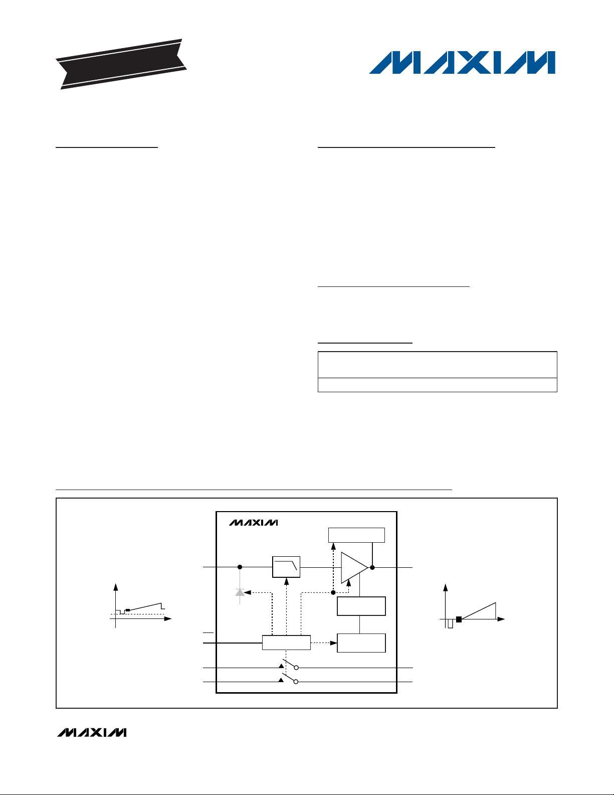
General Description
The MAX9507 amplifies and filters standard-definition
video signals and only consumes 5.8mW quiescent
power and 11.7mW average power. The MAX9507
leverages Maxim’s DirectDrive™ technology to generate a clean, internal negative supply. Combining the
internal negative power supply with the external positive 1.8V supply, the MAX9507 is able to drive a 2V
P-P
video signal into a 150Ω load.
The MAX9507 provides an I2C interface for easy configuration and access to the load status. The MAX9507 can
detect, report, and act upon the change of a video load.
This feature helps reduce overall power consumption by
allowing the system to turn on the video encoder and driver only when a video load is connected to the MAX9507.
With a high power-supply rejection ratio (47dB at
100kHz), the MAX9507 can be powered directly from a
1.8V digital supply. The two integrated single-pole/single-throw (SPST) analog switches are ideal for routing
audio, video, or digital signals.
The input of the MAX9507 can be directly connected to
the output of a video DAC. The MAX9507 also features
a transparent input sync-tip clamp, allowing AC-coupling of input signals with different DC biases.
The MAX9507 has an internal fixed gain of 8. The input
full-scale video signal is nominally 0.25V
P-P
, and the
output full-scale video signal is nominally 2V
P-P
.
Features
♦ 1.8V or 2.5V Single-Supply Operation
♦ Low Power Consumption (5.8mW Quiescent,
11.7mW Average)
♦ Video Load Detection
♦ DirectDrive Sets Video Output Black Level Near
Ground
♦ Dual SPST Analog Switches
♦ Transparent Input Sync-Tip Clamp
♦ I2C Control
Applications
Mobile Phones
Portable Media Players (PMP)
MAX9507
1.8V DirectDrive Video Filter Amplifier with
Load Detection and Dual SPST Analog Switches
________________________________________________________________
Maxim Integrated Products
1
Block Diagram
Ordering Information
PART
PIN-PACKAGE
PKG CODE
TOP
MARK
MAX9507ATE+
16 TQFN-EP* T1633+4 AFH
19-1028; Rev 0; 11/07
For pricing, delivery, and ordering information, please contact Maxim Direct at 1-888-629-4642,
or visit Maxim’s website at www.maxim-ic.com.
Pin Configuration appears at end of data sheet.
Note: This device is specified over the -40°C to +125°C operat-
ing temperature range.
+
Denotes a lead-free package.
*
EP = Exposed pad.
EVALUATION KIT
AVAILABLE
0V
2V
P-P
VIDEO
MAX9507
AV =
8V/V
LINEAR
REGULATOR
CHARGE
PUMP
LOAD DETECT
I2C
TRANSPARENT
CLAMP
OUT
COM1
COM2
IN
LCF
NO1
NO2
250mV
P-P
VIDEO
LPF
Page 2
MAX9507
1.8V DirectDrive Video Filter Amplifier with
Load Detection and Dual SPST Analog Switches
2 _______________________________________________________________________________________
ABSOLUTE MAXIMUM RATINGS
ELECTRICAL CHARACTERISTICS
(VDD= +1.8V, GND = 0V, OUT has RL= 150Ω connected to GND, transparent sync-tip clamp enabled, C1= C2= 1µF, TA= T
MIN
to
T
MAX
, unless otherwise noted. Typical values are at TA= +25°C.) (Note 1)
Stresses beyond those listed under “Absolute Maximum Ratings” may cause permanent damage to the device. These are stress ratings only, and functional
operation of the device at these or any other conditions beyond those indicated in the operational sections of the specifications is not implied. Exposure to
absolute maximum rating conditions for extended periods may affect device reliability.
(Voltages with respect to GND.)
V
DD
...........................................................................-0.3V to +3V
CPGND..................................................................-0.1V to +0.1V
IN................................................................-0.3V to (V
DD
+ 0.3V)
OUT, NO_,
COM_ .................(The greater of V
SS
and -1V) to (VDD+ 0.3V)
SDA, SCL, DEV_ADDR, LCF ....................................-0.3V to +4V
C1P.............................................................-0.3V to (V
DD
+ 0.3V)
C1N .............................................................(V
SS
- 0.3V) to +0.3V
V
SS
............................................................................-3V to +0.3V
Duration of OUT Short Circuit
to V
DD
, GND, and VSS.............................................Continuous
Continuous Current
IN, SDA, SCL, DEV_ADDR, LCF....................................±20mA
NO_, COM_ .................................................................±100mA
Continuous Power Dissipation (T
A
= +70°C)
16-Pin TQFN (derate 15.6mW/°C above +70°C) ........1250mW
Operating Temperature Range .........................-40°C to +125°C
Junction Temperature......................................................+150°C
Storage Temperature Range .............................-65°C to +150°C
Lead Temperature (soldering, 10s) .................................+300°C
Supply Voltage Range V
Supply Current I
Sleep-Mode Supply Current No load 3 µA
Shutdown Supply Current I
Switch-Only Supply Current
Output Load Detect Threshold RL to GND, V
DC-COUPLED INPUT
Input Voltage Range
Input Current I
Input Resistance R
Output Level IN = 80mV -75 +5 +75 mV
AC-COUPLED INPUT
Sync-Tip Clamp Level V
Input-Voltage Swing
Sync Crush
Input Clamping Current IN = 130mV 2 3.2 µA
Line-Time Distortion CIN = 0.1µF 0.2 %
Minimum Input Source
Resistance
Output Level IN = 80mV -75 +5 +75 mV
PARAMETER SYMBOL CONDITIONS MIN TYP MAX UNITS
Guaranteed by PSRR 1.700 2.625 V
DD
DD
SHDN
CLP
No load, full operation
mode
Shutdown mode 0.2
Charge-pump-only mode 520
Guaranteed by outputvoltage swing
IN = 130mV 2 3.2 µA
B
10mV ≤ IN ≤ 250mV 280 kΩ
IN
CIN = 0.1µF -8 0 +11 mV
Guaranteed by outputvoltage swing
Percentage reduction in sync pulse at output,
R
= 37.5Ω, CIN = 0.1µF
SOURCE
SYNC-TIP
Filter enabled 3.1 5.4
Filter disabled 2.9 5.1
< 13mV 200 Ω
1.7V ≤ VDD ≤ 2.625V 0 262.5
2.375V ≤ V
2.625V
1.7V ≤ VDD ≤ 2.625V 252.5
2.375V ≤ V
2.625V
DD
DD
≤
≤
0.2 10 µA
0 325
1.6 %
25 Ω
325
mV
mA
µA
mV
P-P
Page 3

MAX9507
1.8V DirectDrive Video Filter Amplifier with
Load Detection and Dual SPST Analog Switches
_______________________________________________________________________________________ 3
ELECTRICAL CHARACTERISTICS (continued)
(VDD= +1.8V, GND = 0V, OUT has RL= 150Ω connected to GND, transparent sync-tip clamp enabled, C1= C2= 1µF, TA= T
MIN
to
T
MAX
, unless otherwise noted. Typical values are at TA= +25°C.) (Note 1)
DC CHARACTERISTICS
DC Voltage Gain A
Output-Voltage Swing
Power-Supply Rejection Ratio PSRR
Shutdown Input Resistance 0V ≤ IN ≤ V
Output Resistance R
Shutdown Output Resistance 0V ≤ OUT ≤ V
Shutdown OUT Leakage Current 1µA
Output Short-Circuit Current
AC CHARACTERISTICS (FILTER ENABLED)
Standard-Definition
Reconstruction Filter
Differential Gain DG
Differential Phase DP
2T Pulse-to-Bar K Rating
2T Pulse Response 2T = 200ns 0.3 K%
2T Bar Response
Nonlinearity 5-step staircase 0.1 %
Group-Delay Distortion 100kHz ≤ f ≤ 5MHz, OUT = 2V
Peak Signal to RMS Noise 100kHz ≤ f ≤ 5MHz 65 dB
Power-Supply Rejection Ratio PSRR f = 100kHz, 100mV
Output Impedance f = 5MHz, IN = 80mV 7.5 Ω
Shutdown OUT-to-IN Isolation f < 5.5MHz 102 dB
Shutdown IN-to-OUT Isolation f < 5.5MHz 98 dB
PARAMETER SYMBOL CONDITIONS MIN TYP MAX UNITS
Guaranteed by output-voltage swing (Note 2) 7.84 8 8.16 V/V
V
OUT
0V ≤ VIN ≤ 262.5mV,
DC-coupled input
1.7V ≤ VDD ≤ 2.625V
2.375V ≤ V
1.7V ≤ V
load resistors
OUT = 0V, -5mA ≤ I
Sourcing 82
Sinking 32
OUT = 2V
reference frequency is
100kHz
f = 3.58MHz 0.63
f = 4.43MHz 0.93
f = 3.58MHz 0.50
f = 4.43MHz 0.63
2T = 200ns, bar time is 18µs, the beginning
2.5% and the ending 2.5% of the bar time is
ignored
2T = 200ns, bar time is 18µs, the beginning
2.5% and the ending 2.5% of the bar time is
ignored
≤ 2.625V, 0V ≤ VIN ≤ 325mV 2.548 2.6 2.652
DD
≤ 2.625V, measured between 75Ω
DD
DD
DD
,
P-P
0V ≤ V
252.5mV
AC-coupled input
≤ +5mA 0.1 Ω
LOAD
+ 1dB passband
f = 5.5MHz 0
f = 9.3MHz -3
f = 27MHz -49
P-P
P-P
≤
IN
,
P-P
2.058 2.1 2.142
1.979 2.02 2.061
46 60 dB
2.8 MΩ
32 MΩ
7.5 MHz
0.1 K%
0.2 K%
21 ns
47 dB
V
P-P
mA
dB
%
Degrees
Page 4
MAX9507
1.8V DirectDrive Video Filter Amplifier with
Load Detection and Dual SPST Analog Switches
4 _______________________________________________________________________________________
ELECTRICAL CHARACTERISTICS (continued)
(VDD= +1.8V, GND = 0V, OUT has RL= 150Ω connected to GND, transparent sync-tip clamp enabled, C1= C2= 1µF, TA= T
MIN
to
T
MAX
, unless otherwise noted. Typical values are at TA= +25°C.) (Note 1)
)
AC CHARACTERISTICS (FILTER DISABLED)
Small-Signal -3dB Bandwidth OUT = 100mV
Large-Signal -3dB Bandwidth OUT = 2V
Small-Signal 1dB Flatness OUT = 100mV
Large-Signal 1dB Flatness OUT = 2V
Slew Rate OUT = 2V step 35 V/µs
Settling Time to 0.1% OUT = 2V step 230 ns
Differential Gain DG
Differential Phase DP
2T Pulse-to-Bar K Rating
2T Pulse Response 2T = 200ns 0.2 K%
2T Bar Response
Nonlinearity 5-step staircase 0.1 %
Group-Delay Distortion 100kHz ≤ f ≤ 5MHz, OUT = 2V
Peak Signal to RMS Noise 100kHz ≤ f ≤ 5MHz 69 dB
Power-Supply Rejection Ratio PSRR f = 100kHz, 100mV
Output Impedance f = 5MHz, IN = 80mV 7.5 Ω
Shutdown OUT-to-IN Isolation f < 5.5MHz 102 dB
Shutdown IN-to-OUT Isolation f < 5.5MHz 98 dB
CHARGE PUMP
Switching Frequency 325 625 1150 kHz
ANALOG SWITCHES
On-Resistance (Note 3) R
On-Resistance Flatness
(Notes 3, 4)
NO_ Off-Leakage Current
Normal Range
COM_ On-Leakage Current
Normal Range
NO_ Off-Leakage Current,
Extended Range
PARAMETER SYMBOL CONDITIONS MIN TYP MAX UNITS
40.7 MHz
9.8 MHz
32.8 MHz
7.2 MHz
0.1 K%
0.2 K%
15 ns
42 dB
2.3
0.3 1.1
ON
R
FLAT(ON
I
NO_(OFF)N
I
COM_(ON)N
I
NO_(OFF)E
P-P
P-P
P-P
P-P
f = 3.58MHz 0.63
f = 4.43MHz 0.94
f = 3.58MHz 0.50
f = 4.43MHz 0.64
2T = 200ns, bar time is 18µs, the beginning
2.5% and the ending 2.5% of the bar time is
ignored
2T = 200ns, bar time is 18µs, the beginning
2.5% and the ending 2.5% of the bar time is
ignored
P-P
P-P
I
= 10mA,
COM_
V
= 0V
NO_
I
= 10mA
COM_
VDD = 2.625V, V
= 2.3V, 0.3V; TA = +25°C (Notes 3, 5)
V
NO_
V
= 2.625V , V
D D
V
= 0.3V , 2.3V ; TA = + 25° C ( N otes 3, 5)
C OM _
V
= 2.625V , V
D D
V
= + 2.3V , - 0.6V ; TA = + 25° C ( N otes 3, 5)
N O_
Normal range 1.2 2.2
Extended range 1.2 2.2
Normal range,
V
= 0V, 1V, V
NO_
Extended range, V
-0.9V, 0V, +1.2V, V
= 0.3V, 2.3V;
COM_
= hi g h- Z ,
N O_
= - 0.6V , + 2.3V ;
C OM _
DD
NO_
DD
=
-100 +100 nA
-100 +100 nA
-100 +100 nA
%
Degrees
Ω
Ω
Page 5
MAX9507
1.8V DirectDrive Video Filter Amplifier with
Load Detection and Dual SPST Analog Switches
_______________________________________________________________________________________ 5
ELECTRICAL CHARACTERISTICS (continued)
(VDD= +1.8V, GND = 0V, OUT has RL= 150Ω connected to GND, transparent sync-tip clamp enabled, C1= C2= 1µF, TA= T
MIN
to
T
MAX
, unless otherwise noted. Typical values are at TA= +25°C.) (Note 1)
COM_ On-Leakage Current,
Extended Range
Turn-On Time t
Turn-Off Time t
Charge Injection Q
Off-Isolation V
On-Channel -3dB Bandwidth BW
Total Harmonic Distortion THD V
Charge-Pump Noise Extended range, RL = 50Ω 1.2 mV
NO_ Off-Capacitance C
Switch On-Capacitance C
CROSSTALK
Switch to Switch
PARAMETER SYMBOL CONDITIONS MIN TYP MAX UNITS
V
I
COM_(ON)E
ON
OFF
ISO
OFF
ON
= 2.625V , V
D D
V
= - 0.6V , + 2.3V ; TA = + 25°C ( N otes 3, 5)
C OM _
V
= 0.9V, RL = 300Ω, CL = 35pF,
NO_
Figure 1 (Note 6)
V
= 0.9V, RL = 300Ω, CL = 35pF,
NO_
Figure 1 (Note 6)
V
= 0.9V, R
GEN
Figure 2
V
= 1V
NO_
C
= 5pF, Figure 1
L
V
NO_
= 5pF, Figure 1
C
L
COM_
P-P
= 0dBm, R
= 1V
f = 1MHz 21 pF
f = 1MHz 53 pF
Switch 1, 2 closed;
V
= 1V
NO_
= 5pF, Figure 1
C
L
P-P
= hi g h- Z ,
N O_
-100 +100 nA
310 ns
372 ns
= 0Ω, CL = 1nF,
GEN
, RL = 50Ω,
f = 10MHz 49
60 pC
f = 1MHz 69
SOURCE
, RL = 600Ω 0.037 %
P-P
= 50Ω, RL = 50Ω,
280 MHz
f = 10MHz -71
, RL = 50Ω,
f = 1MHz -88
dB
dB
P-P
NO_ to OUT
Switch 1, 2 open; video
circuitry enabled,
= 1V
V
NO_
P-P
f = 10MHz -44
dB
f = 1MHz -78
Switch 1, 2 closed; video circuitry enabled,
OUT to NO_
IN to COM_
f = 20kHz, OUT = 2V
C
= 5pF
L
S w i tch 1, 2 cl osed ; vi d eo ci r cui tr y d i sab l ed ,
f = 20kHz, IN = 0.25V
, RL = 50Ω,
P-P
, RL = 600Ω
P-P
-94 dB
-89 dB
Switch 1, 2 closed; video circuitry enabled,
OUT to COM_
f = 20kHz, OUT = 2V
= 5pF
C
L
, RL = 50Ω,
P-P
-94 dB
CMOS DIGITAL INPUTS (SDA, SCL, DEV_ADDR)
Input Low Voltage V
Input High Voltage V
IL
IH
0.7 x
V
DD
0.3 x
V
DD
V
V
Input Hysteresis 275 mV
Input Leakage Current IIL, I
Input Capacitance C
IH
IN
-10 +10 µA
15 pF
Page 6
MAX9507
1.8V DirectDrive Video Filter Amplifier with
Load Detection and Dual SPST Analog Switches
6 _______________________________________________________________________________________
Note 1: All devices are 100% production tested at TA = +25°C. Specifications over temperature are guaranteed by design.
Note 2: Voltage gain (A
V
) is a two-point measurement in which the output-voltage swing is divided by the input-voltage swing.
Note 3: Normal range: charge pump disabled. Extended range: charge pump enabled. In extended range mode, the switch input
can swing from -0.9V to V
DD
.
Note 4: Flatness is defined as the difference between the maximum and minimum values of on-resistance as measured at the speci-
fied voltages.
Note 5: Not production tested, guaranteed by design.
Note 6: t
ON
and t
OFF
are measured from the end of the writing of register 0x00 until COM reaches 90% of the output voltage. See
Figure 1.
Note 7: C
B
is in picofarads.
ELECTRICAL CHARACTERISTICS (continued)
(VDD= +1.8V, GND = 0V, OUT has RL= 150Ω connected to GND, transparent sync-tip clamp enabled, C1= C2= 1µF, TA= T
MIN
to
T
MAX
, unless otherwise noted. Typical values are at TA= +25°C.) (Note 1)
DIGITAL OUTPUTS (SDA, LCF)
Output Low Voltage V
Output High Leakage Current I
SERIAL INTERFACE TIMING (Figure 3)
Serial Clock Frequency f
Bus Free Time Between STOP
and START Conditions
Hold Time (Repeated) START
Condition
SCL Pulse-Width Low t
SCL Pulse-Width High t
Setup Time for a Repeated
START Condition
Data Hold Time t
Data Setup Time t
Bus Capacitance C
SDA and SCL Receiving Rise
Time
SDA and SCL Receiving Fall
Time
SDA Transmitting Fall Time t
Setup Time for STOP Condition t
Pulse Width of Suppressed Spike t
PARAMETER SYMBOL CONDITIONS MIN TYP MAX UNITS
VDD > 2V 0.4
B
IOL = 3mA
V
= V
OUT
(Note 7)
(Note 7)
(Note 7)
DD
V
< 2V
DD
0 400 kHz
1.3 µs
0.6 µs
1.3 µs
0.6 µs
0.6 µs
0 900 ns
100 ns
20 +
0.1C
B
20 +
0.1C
B
VDD = 1.7V
= 2.625V 0 250
V
DD
20 +
0.1C
B
0.6 µs
050ns
0.2 x
V
DD
1µA
400 pF
300 ns
300 ns
250
OL
OH
SCL
t
BUF
t
HD,STA
LOW
HIGH
t
SU,STA
HD,DAT
SU,DAT
t
R
t
F
F
SU,STO
SP
V
ns
Page 7

MAX9507
1.8V DirectDrive Video Filter Amplifier with
Load Detection and Dual SPST Analog Switches
_______________________________________________________________________________________ 7
Test Circuits/Timing Diagrams
Figure 1. Analog Switch Test Circuit
Figure 2. Analog Switch Charge Injection
Figure 3. I2C Serial-Interface Timing Diagram
V
DD
V
DD
MAX9507
NO_
V
NO_
2
C
I
GND
SCL
SDA
MAX9507
R
GEN
NO_
V
GEN
GND
SDA
COM_
V
DD
V
DD
2
I
WRITE
SDA
REGISTER 00H
V
COM_
C
COM_
C
SCL
R
L
L
V
C
L
COM_
V
COM_
V
COM_
SWITCH
STATE
0V
OFF
50%
t
ON
90%
Q = CL x ΔV
WRITE
REGISTER 00H
COM_
ON
t
OFF
90%
ΔV
COM_
OFF
SDA
t
SU,DAT
t
LOW
SCL
t
t
HD,STA
START
CONDITION
HIGH
t
R
t
F
t
HD,DAT
t
SU,STA
START CONDITION
REPEATED
t
HD,STA
t
BUF
t
SP
t
SU,STO
STOP
CONDITION
START
CONDITION
Page 8
MAX9507
1.8V DirectDrive Video Filter Amplifier with
Load Detection and Dual SPST Analog Switches
8 _______________________________________________________________________________________
Typical Operating Characteristics
(VDD= +1.8V, GND = 0V, mode 2 (Table 6), video output has RL= 150Ω connected to GND, video filter enabled, TA= +25°C,
unless otherwise noted.)
SMALL-SIGNAL GAIN
vs. FREQUENCY
MAX9507 toc01
FREQUENCY (Hz)
GAIN (dB)
100M10M1M
-80
-60
-40
-20
0
20
-100
100k 1G
FLTEN = 0
FLTEN = 1
V
OUT
= 100mV
P-P
SMALL-SIGNAL GAIN FLATNESS
vs. FREQUENCY
MAX9507 toc02
FREQUENCY (Hz)
GAIN (dB)
10M1M
-2
-1
0
1
2
-3
100k 100M
FLTEN = 0
FLTEN = 1
V
OUT
= 100mV
P-P
LARGE-SIGNAL GAIN
vs. FREQUENCY
MAX9507 toc03
FREQUENCY (Hz)
GAIN (dB)
100M10M1M
-80
-60
-40
-20
0
20
-100
100k 1G
FLTEN = 0
FLTEN = 1
V
OUT
= 2V
P-P
LARGE-SIGNAL GAIN FLATNESS
vs. FREQUENCY
MAX9507 toc04
FREQUENCY (Hz)
GAIN (dB)
10M1M
-2
1
0
-1
2
-3
100k 100M
V
OUT
= 2V
P-P
FLTEN = 1
FLTEN = 0
LARGE-SIGNAL
GROUP DELAY vs. FREQUENCY
MAX9507 toc05
FREQUENCY (Hz)
DELAY (ns)
100M10M1M
10
20
30
40
50
60
70
80
90
100
0
100k 1G
FLTEN = 0
FLTEN = 1
V
OUT
= 2V
P-P
SMALL-SIGNAL
GROUP DELAY vs. FREQUENCY
MAX9507 toc06
FREQUENCY (Hz)
DELAY (ns)
100M10M1M
10
20
30
40
50
60
70
80
90
100
0
100k 1G
FLTEN = 0
FLTEN = 1
V
OUT
= 100mV
P-P
POWER-SUPPLY REJECTION RATIO
vs. FREQUENCY
MAX9507 toc07
FREQUENCY (Hz)
GAIN (dB)
10M1M100k
-80
-60
-40
-20
0
20
-100
10k 100M
FLTEN = 0
FLTEN = 1
QUIESCENT SUPPLY CURRENT
vs. TEMPERATURE
MAX9507 toc08
TEMPERATURE (°C)
QUIESCENT SUPPLY CURRENT (mA)
1007550250-25
3.0
2.5
3.5
4.0
2.0
-50 125
FLTEN = 1
FLTEN = 0
VOLTAGE GAIN
vs. TEMPERATURE
MAX9507 toc09
TEMPERATURE (°C)
VOLTAGE GAIN (V/V)
1007550250-25
8.05
7.95
7.90
7.85
8.00
8.10
8.15
8.20
7.80
-50 125
Page 9
MAX9507
1.8V DirectDrive Video Filter Amplifier with
Load Detection and Dual SPST Analog Switches
_______________________________________________________________________________________
9
Typical Operating Characteristics (continued)
(VDD= +1.8V, GND = 0V, mode 2 (Table 6), video output has RL= 150Ω connected to GND, video filter enabled, TA= +25°C,
unless otherwise noted.)
OUTPUT VOLTAGE
vs. INPUT VOLTAGE
2.0
1.5
1.0
0.5
0
OUTPUT VOLTAGE (V)
-0.5
-1.0
-1.5
-100 400
INPUT VOLTAGE (mV)
DIFFERENTIAL GAIN AND PHASE
1.2
0.8
0.4
0
-0.4
DIFFERENTIAL GAIN (%)DIFFERENTIAL PHASE (deg)
-0.8
1.2
0.8
0.4
0
-0.4
-0.8
(FLTEN = 0)
FREQUENCY = 3.58MHz
= 71mV
V
IN
13610471 232
DC INPUT LEVEL (mV)
DC INPUT LEVEL (mV)
P-P
200168
20016813610471 232
DIFFERENTIAL GAIN AND PHASE
1.2
0.8
MAX9507 toc10
350300250200150100500-50
0.4
0
-0.4
DIFFERENTIAL GAIN (%)DIFFERENTIAL PHASE (deg)
-0.8
1.2
0.8
0.4
0
-0.4
-0.8
(FLTEN = 1)
FREQUENCY = 3.58MHz
= 71mV
V
IN
13610471 232
DC INPUT LEVEL (mV)
DC INPUT LEVEL (mV)
P-P
200168
20016813610471 232
MAX9507 toc11
DIFFERENTIAL GAIN (%)DIFFERENTIAL PHASE (deg)
DIFFERENTIAL GAIN AND PHASE
(FLTEN = 0)
FREQUENCY = 4.43MHz
= 71mV
V
IN
13610471 232
DC INPUT LEVEL (mV)
DC INPUT LEVEL (mV)
MAX9507 toc14
P-P
200168
20016813610471 232
MAX9507 toc13
-0.4
DIFFERENTIAL GAIN (%)DIFFERENTIAL PHASE (deg)
-0.8
-0.4
-0.8
1.2
0.8
0.4
0
1.2
0.8
0.4
0
DIFFERENTIAL GAIN AND PHASE
1.2
0.8
0.4
0
-0.4
-0.8
1.2
0.8
0.4
0
-0.4
-0.8
(FLTEN = 1)
13610471 232
DC INPUT LEVEL (mV)
DC INPUT LEVEL (mV)
2T RESPONSE
400ns/div
FREQUENCY = 4.43MHz
= 71mV
V
IN
P-P
200168
20016813610471 232
MAX9507 toc15
MAX9507 toc12
IN
100mV/div
0V
OUT
500mV/div
0V
12.5T RESPONSE
400ns/div
MAX9507 toc16
IN
100mV/div
0V
OUT
500mV/div
0V
NTC-7 RESPONSE
10μs/div
MAX9507 toc17
IN
100mV/div
0V
OUT
500mV/div
0V
PAL MULTIBURST
10μs/div
MAX9507 toc18
IN
100mV/div
0V
OUT
1V/div
0V
Page 10

MAX9507
1.8V DirectDrive Video Filter Amplifier with
Load Detection and Dual SPST Analog Switches
10 ______________________________________________________________________________________
Typical Operating Characteristics (continued)
(VDD= +1.8V, GND = 0V, mode 2 (Table 6), video output has RL= 150Ω connected to GND, video filter enabled, TA= +25°C,
unless otherwise noted.)
PAL COLOR BARS
10μs/div
LARGE-SIGNAL PULSE RESPONSE
INPUT (125mV/div)
OUTPUT (1V/div)
ON-RESISTANCE vs. COM_ VOLTAGE
7
6
5
4
3
ON-RESISTANCE (Ω)
2
1
0
0 2.0
(FLTEN = 0)
100ns/div
(NORMAL RANGE)
TA = +125°C
COM_ VOLTAGE (V)
TA = -40°C
TA = +25°C
MAX9507 toc19
MAX9507 toc22
1.81.61.41.21.00.80.60.40.2
IN
100mV/div
0V
OUT
1V/div
0V
MAX9507 toc25
FIELD SQUARE-WAVE RESPONSE
(AC-COUPLED INPUT)
10μs/div
ON-RESISTANCE vs. COM_ VOLTAGE
(NORMAL RANGE)
4.0
3.5
3.0
2.5
2.0
1.5
ON-RESISTANCE (Ω)
1.0
0.5
0
0 3.0
VDD = 1.8V
VDD = 2.5V
COM_ VOLTAGE (V)
ON-RESISTANCE vs. COM_ VOLTAGE
(EXTENDED RANGE)
1.8
1.6
1.4
1.2
1.0
0.8
0.6
ON-RESISTANCE (Ω)
0.4
0.2
0
-1.0 2.0
TA = +125°C
TA = +25°C
TA = -40°C
COM_ VOLTAGE (V)
MAX9507 toc20
2.52.00.5 1.0 1.5
1.51.00.50-0.5
IN
100mV/div
0V
OUT
500mV/div
0V
MAX9507 toc23
MAX9507 toc26
SMALL-SIGNAL PULSE RESPONSE
(FLTEN = 0)
INPUT (6.25mV/div)
OUTPUT (50mV/div)
100ns/div
ON-RESISTANCE vs. COM_ VOLTAGE
(EXTENDED RANGE)
1.6
1.4
1.2
1.0
0.8
0.6
ON-RESISTANCE (Ω)
0.4
0.2
0
-1.0 3.0
VDD = 1.8V
VDD = 2.5V
COM_ VOLTAGE (V)
ANALOG SWITCH LEAKAGE CURRENT
vs. TEMPERATURE (NORMAL RANGE)
6
V
= 2.625V
DD
5
4
3
2
LEAKAGE CURRENT (nA)
1
0
-1
-50 125
TEMPERATURE (°C)
COM
COM
MAX9507 toc21
MAX9507 toc24
2.52.0-0.5 0 0.5 1.0 1.5
MAX9507 toc27
ON
OFF
1007550250-25
Page 11

MAX9507
1.8V DirectDrive Video Filter Amplifier with
Load Detection and Dual SPST Analog Switches
______________________________________________________________________________________
11
Typical Operating Characteristics (continued)
(VDD= +1.8V, GND = 0V, mode 2 (Table 6), video output has RL= 150Ω connected to GND, video filter enabled, TA= +25°C,
unless otherwise noted.)
ANALOG SWITCH LEAKAGE CURRENT
vs. TEMPERATURE (EXTENDED RANGE)
6
V
= 2.625V
DD
5
4
3
2
LEAKAGE CURRENT (nA)
1
0
-1
-50 125
TEMPERATURE (°C)
COM
COM
SWITCH FREQUENCY RESPONSE
5
0
-5
-10
GAIN (dB)
-15
-20
-25
RL = 50Ω
= 5pF
C
L
-30
100k 1G
ON
OFF
1007550250-25
FREQUENCY (Hz)
500
MAX9507 toc28
400
300
200
100
SWITCH CHARGE INJECTION (pC)
0
-1.0 2.0
MAX9507 toc31
100M10M1M
SWITCH CHARGE INJECTION
vs. VOLTAGE
C
LOAD
OPEN = 1
OPEN = 0
SWITCH INPUT VOLTAGE (V)
= 1nF
MAX9507 toc29
SUPPLY CURRENT (nA)
1.51.00 0.5-0.5
SWITCH OFF-ISOLATION
0
-10
-20
-30
-40
-50
GAIN (dB)
-60
-70
-80
-90
-100
100k 1G
SWITCH-ONLY SUPPLY CURRENT
vs. TEMPERATURE (NORMAL RANGE)
300
250
200
150
100
50
0
-50 125
TEMPERATURE (°C)
SPEN = 0
CPEN = 0
vs. FREQUENCY
MAX9507 toc32
100M10M1M
FREQUENCY (Hz)
MAX9507 toc30
1007550250-25
SWITCH-TO-SWITCH CROSSTALK
vs. FREQUENCY
0
-20
-40
-60
ISOLATION (dB)
-80
-100
-120
100k 100M
FREQUENCY (Hz)
10M1M
MAX9507 toc33
TOTAL HARMONIC DISTORTION PLUS NOISE
vs. FREQUENCY
0.1
V
= 2V
IN
P-P
R
= 600Ω
LOAD
THD+N (%)
0.01
FREQUENCY (Hz)
10k1k10010 100k
MAX9507 toc34
Page 12

MAX9507
1.8V DirectDrive Video Filter Amplifier with
Load Detection and Dual SPST Analog Switches
12 ______________________________________________________________________________________
Pin Description
Detailed Description
The MAX9507 represents Maxim’s second-generation
of DirectDrive video amplifiers that meet the requirements of current and future portable equipment:
• 1.8V Operation: Eliminate the need for 3.3V supply in
favor of lower supply voltages.
• Lower Power Consumption: The MAX9507 reduces
average power consumption by up to 75% compared to the 3.3V first generation (MAX9503/
MAX9505).
• Internal Fixed Gain of 8: As the supply voltages drop
for system chips on deep submicron processes, the
video DAC can no longer create a 1V
P-P
signal at its
output, and the gain of 2 found in the previous generation of video filter amplifiers is not enough.
• Load Reporting: The MAX9507 senses the presence
of a video load. For portable devices, a video load is
not connected most of the time, and turning off the
video encoder saves power. Another benefit of load
reporting is a simpler user interface, eliminating the
need to browse through menus to activate the video
output. Instead, the equipment will automatically
enable this feature.
• Dual SPST Analog Switches: The two analog switches are ideal for routing additional audio, video, or
digital signals.
DirectDrive technology is necessary for a voltage-mode
amplifier to output a 2V
P-P
video signal from a 1.8V
supply. The integrated inverting charge pump creates
a negative supply that increases the output range and
gives the video amplifier enough headroom to drive a
2V
P-P
video signal into a 150Ω load.
DirectDrive
Background
Integrated video filter amplifier circuits operate from a
single supply. The positive power supply usually creates video output signals that are level-shifted above
ground to keep the signal within the linear range of the
output amplifier. For applications where the positive DC
level is not acceptable, a series capacitor can be
inserted in the output connection in an attempt to eliminate the positive DC level shift. The series capacitor
cannot truly level shift a video signal because the average level of the video varies with picture content. The
series capacitor biases the video output signal around
ground, but the actual level of the video signal can vary
significantly depending upon the RC time constant and
the picture content.
PIN NAME FUNCTION
1 IN Video Input
2 SDA I2C-Compatible Serial-Data Input/Output
3 SCL I2C-Compatible Serial-Clock Input
4 DEV_ADDR I2C Device Address Input. Connect DEV_ADDR to GND, VDD, SCL, or SDA. See Table 4.
5VDDPositive Power Supply. Bypass with a 0.1µF capacitor to GND.
6 C1P Charge-Pump Flying Capacitor Positive Terminal. Connect a 1µF capacitor from C1P to C1N.
7 CPGND Charge-Pump Ground
8 C1N Charge-Pump Flying Capacitor Negative Terminal. Connect a 1µF capacitor from C1P to C1N.
9VSSCharge-Pump Negative Power Supply. Bypass with a 1µF capacitor to GND.
10 OUT Video Output
11 GND Ground
12 LCF Load Change Flag. Open-drain, active-low signal indicates when a video load change occurs.
13 NO1 Normally Open Terminal 1
14 COM1 Common Terminal 1
15 COM2 Common Terminal 2
16 NO2 Normally Open Terminal 2
— EP Exposed Pad. EP is internally connected to GND. Connect EP to GND.
Page 13

The series capacitor creates a highpass filter. Since the
lowest frequency in video is the frame rate, which can be
between 24Hz and 30Hz, the pole of the highpass filter
should ideally be an order of magnitude lower in frequency than the frame rate. Therefore, the series capacitor must be very large, typically from 220µF to 3000µF.
For space-constrained equipment, the series capacitor
is unacceptable. Changing from a single series capacitor to a SAG network that requires two smaller capacitors
can only reduce space and cost slightly.
The series capacitor in the usual output connection
also prevents damage to the output amplifier if the connector is shorted to a supply or to ground. While the
output connection of the MAX9507 does not have a
series capacitor, the MAX9507 will not be damaged if
the connector is shorted to a supply or to ground (see
the
Short-Circuit Protection
section).
Video Amplifier
If the full-scale video signal from a video DAC is
250mV, the black level of the video signal created by
the video DAC is around 75mV. The MAX9507 shifts the
black level to near ground at the output so that the
active video is above ground and the sync is below
ground. The amplifier needs a negative supply for its
output stage to remain in its linear region when driving
sync below ground.
The MAX9507 has an integrated charge pump and linear regulator to create a low-noise negative supply
from the positive supply voltage. The charge pump
inverts the positive supply to create a raw negative voltage that is then fed into the linear regulator filtering out
the charge-pump noise.
Comparison Between DirectDrive Output
and AC-Coupled Output
The actual level of the video signal varies less with a
DirectDrive output than an AC-coupled output. The
average video signal level can change greatly depending upon the picture content. With an AC-coupled output, the average level will change according to the time
constant formed by the series capacitor and series
resistance (usually 150Ω). For example, Figure 4 shows
an AC-coupled video signal alternating between a
completely black screen and a completely white
screen. Notice the excursion of the video signal as the
screen changes.
With the DirectDrive amplifier, the black level is held at
ground. The video signal is constrained between -0.3V
to +0.7V. Figure 5 shows the video signal from a
DirectDrive amplifier with the same input signal as the
AC-coupled system.
Video Reconstruction Filter
The MAX9507 includes an internal five-pole,
Butterworth lowpass filter to condition the video signal.
The reconstruction filter smoothes the steps and
reduces the spikes created whenever the DAC output
changes value. In the frequency domain, the steps and
spikes cause images of the video signal to appear at
multiples of the sampling clock frequency. The reconstruction filter typically has ±1dB passband flatness of
7.3MHz and 48dB attenuation at 27MHz.
MAX9507
1.8V DirectDrive Video Filter Amplifier with
Load Detection and Dual SPST Analog Switches
______________________________________________________________________________________ 13
Figure 4. AC-Coupled Output
Figure 5. DirectDrive Output
0V
0V
INPUT
OUTPUT
2ms/div
INPUT
OUTPUT
2ms/div
Page 14

MAX9507
1.8V DirectDrive Video Filter Amplifier with
Load Detection and Dual SPST Analog Switches
14 ______________________________________________________________________________________
Transparent Sync-Tip Clamp
The MAX9507 contains an integrated, transparent
sync-tip clamp. When using a DC-coupled input, the
sync-tip clamp does not affect the input signal, as long
as it remains above ground. When using an AC-coupled input, the sync-tip clamp automatically clamps the
input signal to ground, preventing it from going lower. A
small current of 2µA pulls down on the input to prevent
an AC-coupled signal from drifting outside the input
range of the device.
Using an AC-coupled input results in some additional
variation of the black level at the output. Applying a
voltage above ground to the input pin of the device
always produces the same output voltage, regardless
of whether the input is DC- or AC-coupled. However,
since the sync-tip clamp level (V
CLP
) can vary over a
small range, the video black level at the output of the
device when using an AC-coupled input can vary by an
additional amount equal to the V
CLP
multiplied by the
DC voltage gain (AV).
Dual SPST Analog Switches
The MAX9507 has dual SPST analog switches for routing additional audio, video, digital, and other signals.
The switches are selected through the I2C interface.
SW1EN (register 0x00, bit B6) and SW2EN (register
0x00, bit B7) control the analog switches. See the
I2C
Registers and Bit Descriptions
section. The dual analog
switches operate in either normal or extended range. In
normal range, the part is in shutdown and the analog
switches can handle signals between GND and V
DD
. In
extended range, the charge pump and linear regulator
are on and the analog switches can handle signals
between -0.9V and V
DD
.
Short-Circuit Protection
The MAX9507 typical operating circuit includes a 75Ω
back-termination resistor that limits short-circuit current
if an external short is applied to the video output. The
MAX9507 also features internal output short-circuit protection to prevent device damage in prototyping and
applications where the amplifier output can be directly
shorted.
Powering On/Off the MAX9507
The MAX9507 powers on in a low-power shutdown
mode with the analog switches open and the video signal path, charge pump, and load detection circuitry
disabled. It is good practice to configure the operating
mode of the signal path before enabling it. This may
include selecting the sync-tip clamp and video filter.
Setting CPEN = 1 (register 0x00, bit B0) enables the
charge pump. The charge pump must be fully operational before the signal path will be functional. Setting
SPEN = 1 (register 0x00, bit B1) enables the signal
path. Both SPEN and CPEN may be set at the same
time and internal control circuitry will monitor the
charge pump and enable the signal path at the appropriate time.
The analog switches can be turned on or off at any
time, regardless of the state of the charge pump or signal path. However, the signal range is limited from GND
to VDDwhen the charge pump is disabled.
The MAX9507 can be placed in a low-power shutdown
mode by setting SPEN = 0 and CPEN = 0.
Video Load Detection Circuitry
The MAX9507 contains video load detection circuitry at
the video output, enabling efficient power consumption
based on the actual presence of a video load. Setting
the automatic signal path enable bit, ASPEN = 1 (register 0x01, bit B1) or the automatic charge-pump enable
bit, ACPEN = 1 (register 0x01, bit B0) enables the load
detection feature. The LOAD bit (register 0x01, bit B7)
indicates the load status.
To enable complete, automatic control of the part, set
ASPEN = ACPEN = 1 and SPEN = CPEN = 0. In this
state, when an output load is connected to the amplifier, the signal path and charge pump fully turn on and
stay on until the output load is disconnected. If an output load is not connected to the amplifier, then the signal path and charge pump remain in a low-power sleep
mode while continuing to check if a load is connected.
Setting SPEN = 1 or CPEN = 1 overrides the corresponding ASPEN or ACPEN bits, enabling the block
regardless of the detected video load status.
The LOAD bit indicates the latest video load status. All
changes to the video load status are debounced typically 128ms to eliminate false load-detect events.
Setting the load change flag enable bit, LCFEN = 1 (register 0x01, bit B3), and enabling the load detection feature (ASPEN = 1 or ACPEN = 1) enables the open-drain
LCF output. LCF asserts low whenever the LOAD bit
changes state. It remains low until the LOAD bit (register
0x01) is read. LCF can be used as an interrupt to notify
the system that the load status has changed.
Page 15

MAX9507
1.8V DirectDrive Video Filter Amplifier with
Load Detection and Dual SPST Analog Switches
______________________________________________________________________________________ 15
Sleep Mode
If a video load is not connected to the amplifier, the
MAX9507 remains in a low-power sleep mode. The
load-sense circuitry checks for a load eight times per
second by connecting an internal 7.5kΩ pullup resistor
to the output for 1ms. If the output is pulled up, no load
is present. If the output stays low, a load is connected,
and the automatic control circuitry enables the appro-
priate blocks. When the amplifier is on, it continually
checks if the load has been disconnected by detecting
if the amplifier is sinking current during a horizontal line
time. Therefore, a black-burst signal (or input signal
< 13mV) is required to maintain the detected load status. If the load is disconnected, the device returns to
the low-power sleep mode.
Common Modes of Operation
X = Don’t care.
I2C Registers and Bit Descriptions
Table 1. Register Map
NO. MODE ASPEN ACPEN SPEN CPEN
Shutdown mode.
1
Switches in normal range.
Load-detect function disabled.
Full operation mode.
Video, charge pump, and regulator on.
2
Switches in extended range.
Charge-pump-only mode.
3
Charge pump and regulator on, video off.
Switches in extended range.
Sleep mode.
Video, charge pump, and regulator automatic.
4
Switches in extended range only when the charge
pump is on.
Load-detect function enabled.
Charge pump and regulator on, video automatic.
Switches in extended range.
5
Load-detect function enabled.
0000
XX11
XX01
1100
1001
REGISTER
ADDRESS
0x00 Configuration SW2EN SW1EN 0 STEN FLTEN 0 SPEN CPEN 0x00
0x01
REGISTER B7 B6 B5 B4 B3 B2 B1 B0
Video Load
Detect
LOAD 0 0 0 LCFEN 0 ASPEN ACPEN 0x00
POWER-ON
RESET
STATE
Page 16

MAX9507
1.8V DirectDrive Video Filter Amplifier with
Load Detection and Dual SPST Analog Switches
16 ______________________________________________________________________________________
I2C Serial Interface
The MAX9507 features an I2C/SMBus™-compatible, 2wire serial interface consisting of a serial-data line (SDA)
and a serial-clock line (SCL). SDA and SCL facilitate
communication between the MAX9507 and the master at
clock rates up to 400kHz. Figure 3 shows the 2-wire interface timing diagram. The master generates SCL and initiates data transfer on the bus. A master device writes data
to the MAX9507 by transmitting a START (S) condition,
the proper slave address with the R/W bit set to 0, followed by the register address and then the data word.
Each transmit sequence is framed by a START and a
STOP (P) condition. Each word transmitted to the
MAX9507 is 8 bits long and is followed by an acknowledge clock pulse. A master reads from the MAX9507 by
transmitting the slave address with the R/W bit set to 0,
the register address of the register to be read, a REPEATED START (Sr) condition, the slave address with the R/W
bit set to 1, followed by a series of SCL pulses. The
MAX9507 transmits data on SDA in sync with the mastergenerated SCL pulses. The master acknowledges receipt
of each byte of data. Each read sequence is framed by a
START or REPEATED START condition, an acknowledge
or a not acknowledge, and a STOP condition. SDA operates as both an input and an open-drain output. A pullup
resistor, typically greater than 500Ω, is required on the
SDA bus. SCL operates as only an input. A pullup resistor, typically greater than 500Ω, is required on SCL if
there are multiple masters on the bus, or if the master in a
single-master system has an open-drain SCL output.
Table 2. Configuration Register (0x00)
*
Internal control circuitry prevents the signal path from turning on until the charge pump has been enabled and has settled.
Table 3. Video Load-Detect Register (0x01)
*
Read-only bit indicating the load status when the video load-detect circuitry is enabled (ASPEN = 1 or ACPEN = 1). When LCFEN = 1,
reading this bit will clear the LCF flag.
**
If SPEN = 0, then the signal path will be automatically enabled when a video load is detected and the charge pump has been
enabled and has settled.
***
If CPEN = 0, then the charge pump will be automatically enabled when a video load is detected.
SMBus is a trademark of Intel Corp.
BIT NAME FUNCTION
B7 SW2EN
B6 SW1EN
B4 STEN
B3 FLTEN
B1 SPEN
B0 CPEN
BIT NAME FUNCTION
B7 LOAD*
B3 LCFEN
B1 ASPEN
B0 ACPEN
1 = Analog switch 2 closed.
0 = Analog switch 2 open.
1 = Analog switch 1 closed.
0 = Analog switch 1 open.
1 = Transparent sync-tip clamp enabled, the input can be DC- or AC-coupled.
0 = Transparent sync-tip clamp disabled, the input must be DC-coupled.
1 = Video filter enabled.
0 = Video filter disabled (bypassed).
1 = Signal path enabled* (SPEN overrides the ASPEN setting).
0 = Signal path disabled.
1 = Charge pump enabled (CPEN overrides the ACPEN setting).
0 = Charge pump disabled.
1 = Load detected.
0 = No load detected.
1 = Changes to the video load will trigger LCF to pull low.
0 = Changes to the video load are not reported.
1 = Enable automatic control of the video signal path**.
0 = Disable automatic control of the video signal path.
1 = Enable automatic control of the charge pump***.
0 = Disable automatic control of the charge pump.
Page 17

Series resistors in line with SDA and SCL are optional.
Series resistors protect the digital inputs of the MAX9507
from high-voltage spikes on the bus lines, and minimize
crosstalk and undershoot of the bus signals.
Bit Transfer
One data bit is transferred during each SCL cycle. The
data on SDA must remain stable during the high period
of the SCL pulse. Changes in SDA while SCL is high
are control signals (see the
START and STOP
Conditions
section). SDA and SCL idle high when the
I2C bus is not busy.
START and STOP Conditions
SDA and SCL idle high when the bus is not in use. A
master initiates communication by issuing a START condition. A START condition is a high-to-low transition on
SDA with SCL high. A STOP condition is a low-to-high
transition on SDA while SCL is high (Figure 6). A START
condition from the master signals the beginning of a
transmission to the MAX9507. The master terminates
transmission, and frees the bus, by issuing a STOP condition. The bus remains active if a REPEATED START
condition is generated instead of a STOP condition.
Early STOP Conditions
The MAX9507 recognizes a STOP condition at any point
during data transmission except if the STOP condition
occurs in the same high pulse as a START condition. For
proper operation, do not send a STOP condition during
the same SCL high pulse as the START condition.
Slave Address
The slave address is defined as the 7 most significant
bits (MSBs) followed by the read/write (R/W) bit. Set the
R/W bit to 1 to configure the MAX9507 to read mode.
Set the R/W bit to 0 to configure the MAX9507 to write
mode. The slave address is always the first byte of
information sent to the MAX9507 after a START or a
REPEATED START condition. The MAX9507 slave
address is configurable with DEV_ADDR. Table 4
shows the possible slave addresses for the MAX9507.
Acknowledge
The acknowledge bit (ACK) is a clocked 9th bit that the
MAX9507 uses to handshake receipt of each byte of data
when in write mode (see Figure 7). The MAX9507 pulls
down SDA during the entire master-generated ninth clock
pulse if the previous byte is successfully received.
Monitoring ACK allows for detection of unsuccessful data
transfers. An unsuccessful data transfer occurs if a
receiving device is busy or if a system fault has occurred.
In the event of an unsuccessful data transfer, the bus
master may retry communication. The master pulls down
SDA during the ninth clock cycle to acknowledge receipt
of data when the MAX9507 is in read mode. An acknowledge is sent by the master after each read byte to allow
data transfer to continue. A not acknowledge is sent
when the master reads the final byte of data from the
MAX9507, followed by a STOP condition.
MAX9507
1.8V DirectDrive Video Filter Amplifier with
Load Detection and Dual SPST Analog Switches
______________________________________________________________________________________ 17
Figure 6. START, STOP, and REPEATED START Conditions
Figure 7. Acknowledge
Table 4. Slave Address
DEV_ADDR B7 B6 B5 B4 B3 B2 B1 B0
GND 1001100R/W 0x98 0x99
V
DD
SCL 1001110R/W 0x9C 0x9D
SDA 1001111R/W 0x9E 0x9F
SCL
SDA
1001101R/W 0x9A 0x9B
SSrP
START
CONDITION
SCL
SDA
WRITE ADDRESS
(hex)
1
289
NOT ACKNOWLEDGE
READ ADDRESS
(hex)
CLOCK PULSE FOR
ACKNOWLEDGMENT
ACKNOWLEDGE
Page 18

MAX9507
1.8V DirectDrive Video Filter Amplifier with
Load Detection and Dual SPST Analog Switches
18 ______________________________________________________________________________________
Write Data Format
A write to the MAX9507 consists of transmitting a
START condition, the slave address with the R/W bit set
to 0, one data byte to configure the internal register
address pointer, one or more data bytes, and a STOP
condition. Figure 8 illustrates the proper frame format
for writing one byte of data to the MAX9507. Figure 9
illustrates the frame format for writing n-bytes of data to
the MAX9507.
The slave address with the R/W bit set to 0 indicates
that the master intends to write data to the MAX9507.
The MAX9507 acknowledges receipt of the address
byte during the master-generated ninth SCL pulse.
The second byte transmitted from the master configures the MAX9507’s internal register address pointer.
The pointer tells the MAX9507 where to write the next
byte of data. An acknowledge pulse is sent by the
MAX9507 upon receipt of the address pointer data.
The third byte sent to the MAX9507 contains the data
that will be written to the chosen register. An acknowledge pulse from the MAX9507 signals receipt of the
data byte. The address pointer autoincrements to the
next register address after each received data byte.
This autoincrement feature allows a master to write to
sequential register address locations within one continuous frame. The master signals the end of transmission
by issuing a STOP condition.
Read Data Format
The master presets the address pointer by first sending
the MAX9507’s slave address with the R/W bit set to 0
followed by the register address after a START condition. The MAX9507 acknowledges receipt of its slave
address and the register address by pulling SDA low
during the ninth SCL clock pulse. A REPEATED START
condition is then sent followed by the slave address
with the R/W bit set to 1. The MAX9507 transmits the
contents of the specified register. Transmitted data is
valid on the rising edge of the master-generated serial
clock (SCL). The address pointer autoincrements after
each read data byte. This autoincrement feature allows
all registers to be read sequentially within one continuous frame. A STOP condition can be issued after any
number of read data bytes. If a STOP condition is
issued followed by another read operation, the first
Figure 8. Writing a Byte of Data to the MAX9507
Figure 9. Writing n-Bytes of Data to the MAX9507
ACKNOWLEDGE FROM MAX9507
ACKNOWLEDGE FROM MAX9507
S AA
ACKNOWLEDGE FROM MAX9507
S
SLAVE ADDRESS
R/W
0SLAVE ADDRESS REGISTER ADDRESS DATA BYTE
R/W
ACKNOWLEDGE FROM MAX9507
A
REGISTER ADDRESS
ACKNOWLEDGE FROM MAX9507
ACKNOWLEDGE FROM MAX9507
A
DATA BYTE 1
1 BYTE
AUTOINCREMENT INTERNAL
REGISTER ADDRESS POINTER
B1 B0B3 B2B5 B4B7 B6
A
P
1 BYTE
AUTOINCREMENT INTERNAL
REGISTER ADDRESS POINTER
ACKNOWLEDGE FROM MAX9507
B1 B0B3 B2B5 B4B7 B6
A0
DATA BYTE n
1 BYTE
B1 B0B3 B2B5 B4B7 B6
A
P
Page 19

MAX9507
1.8V DirectDrive Video Filter Amplifier with
Load Detection and Dual SPST Analog Switches
______________________________________________________________________________________ 19
data byte to be read will be from the register address
location set by the previous transaction and not 0x00,
and subsequent reads will autoincrement the address
pointer until the next STOP condition. Attempting to
read from register addresses higher than 0x01 results
in repeated reads from a dummy register containing
0xFF data. The master acknowledges receipt of each
read byte during the acknowledge clock pulse. The
master must acknowledge all correctly received bytes
except the last byte. The final byte must be followed by
a not acknowledge from the master and then a STOP
condition. Figures 10 and 11 illustrate the frame format
for reading data from the MAX9507.
Applications Information
Power Consumption
The quiescent power consumption and average power
consumption of the MAX9507 is remarkably low
because of 1.8V operation and DirectDrive technology.
Quiescent power consumption is defined when the
MAX9507 is operating without load. In this case, the
MAX9507 consumes about 5.8mW. Average power
consumption, which is defined when the MAX9507 drives a 150Ω load to ground with a 50% flat field, is
about 11.7mW. Table 5 shows the power consumption
with different video signals. The supply voltage is 1.8V
and OUT drives a 150Ω load to ground.
Notice that the two extremes in power consumption occur
with a video signal that is all black and a video signal that
is all white. The power consumption with 75% color bars
and 50% flat field lies in between the extremes.
Figure 11. Reading n-Bytes of Indexed Data from the MAX9507
Figure 10. Reading One Indexed Byte of Data from the MAX9507
Table 5. MAX9507 Power Consumption with Different Video Signals
ACKNOWLEDGE FROM MAX9507
SA
R/W
ACKNOWLEDGE FROM MAX9507
0
ACKNOWLEDGE FROM MAX9507
Sr 1SLAVE ADDRESS REGISTER ADDRESS SLAVE ADDRESS DATA BYTE
NOT ACKNOWLEDGE FROM MASTER
AA
R/WREPEATED START
A
1 BYTE
AUTOINCREMENT INTERNAL
REGISTER ADDRESS POINTER
P
ACKNOWLEDGE FROM MAX9507
SA
R/W
ACKNOWLEDGE FROM MAX9507
0
REPEATED START
ACKNOWLEDGE FROM MAX9507
Sr 1SLAVE ADDRESS REGISTER ADDRESS SLAVE ADDRESS DATA BYTE
AA
R/W
VIDEO SIGNAL
All Black Screen 6.7 6.2
All White Screen 18.2 17.9
75% Color Bars 11.6 11.0
50% Flat Field 11.7 11.3
MAX9507 POWER CONSUMPTION WITH
FILTER ENABLED (mW)
MAX9507 POWER CONSUMPTION WITH
FILTER DISABLED (mW)
A
1 BYTE
AUTOINCREMENT INTERNAL
REGISTER ADDRESS POINTER
Page 20

MAX9507
Interfacing to Video DACs that Produce
Video Signals Larger than 0.25V
P-P
Devices designed to generate 1V
P-P
video signals at
the output of the video DAC can still work with the
MAX9507. Most video DACs source current into a
ground-referenced resistor, which converts the current
into a voltage. Figure 12 shows a video DAC that creates a video signal from 0 to 1V across a 150Ω resistor.
The following video filter amplifier has a 2V/V gain so
that the output is 2V
P-P
.
The MAX9507 expects input signals that are 0.25V
P-P
nominally. The same video DAC can be made to work
with the MAX9507 by scaling down the 150Ω resistor to
a 37.5Ω resistor, as shown in Figure 13. The 37.5Ω resistor is one-quarter the size of the 150Ω resistor, resulting
in a video signal that is one-quarter the amplitude.
Changing Between Video Output and
Microphone Input on a Single Connector
Figure 14 shows how a single pole on a mobile phone
jack can be used for transmitting a video signal to a
television or receiving the signal from the microphone
of a headset. To transmit a video signal, open SW1 and
enable the video circuitry. To receive a signal from a
microphone, close SW1 and disable the video circuitry.
Switching Between Video
and Digital Signals
Figure 15 shows how the dual SPST analog switches
and the high-impedance output of the video amplifier
enable video transmission, digital transmission, and
digital reception all on a single pole of a connector. To
transmit a video signal, open SW1 and SW2 and enable
the video circuitry. To receive a digital signal, close
SW1, open SW2, and disable the video circuitry. To
transmit a digital signal, open SW1, close SW2, and
disable the video circuitry.
Selecting Between Two Video Sources
The analog switches can multiplex between two video
sources. For example, a mobile phone might have an
application processor with an integrated video encoder
and a mobile graphics processor with an integrated
video encoder, each creating a composite video signal
that is between 0 and 0.25V. Figure 16 shows this application in which the MAX9507 chooses between two internal video sources. The two analog switches can be used
as a 2:1 multiplexer to select which video DAC output is
filtered, amplified, and driven out to the connector.
If the analog switches are in extended mode, then they
can also be used to select between two external video
signals, as shown in Figure 17. The external video signals are usually between -2V and +2V. The resistor network divides the external signal by a factor of four,
thereby reducing the signal to between -0.5V and +0.5V
(see the
Anti-Alias Filter
section for an explanation on
why the resistor-divider network is necessary). In extended mode, the analog switch can easily handle this bipolar input signal, even if the supply voltage is 1.8V.
1.8V DirectDrive Video Filter Amplifier with
Load Detection and Dual SPST Analog Switches
20 ______________________________________________________________________________________
Figure 12. Video DAC Generates a 1V
P-P
Signal Across a
150
Ω
Resistor Connected to Ground
Figure 13. Video DAC Generates a 0.25V
P-P
Signal Across a
37.5
Ω
Resistor Connected to Ground
IMAGE
PROCESSOR
ASIC
DAC
IMAGE
PROCESSOR
ASIC
DAC
0 TO 1V
LPF
150Ω
MAX9507
0 TO 0.25V
LPF
37.5Ω
2V
2V/V
2V
8V/V
75Ω
P-P
75Ω
P-P
Page 21

MAX9507
1.8V DirectDrive Video Filter Amplifier with
Load Detection and Dual SPST Analog Switches
______________________________________________________________________________________ 21
Figure 14. Video Output Configuration
V
CC
V
CC
MIC
BASEBAND
IC
BIAS
MIC
AMP
MAX9507
V
CC
SDA
SCL
LCF
2
C INTERFACE
I
SW1 COM1NO1
SW2 COM2NO2
LOAD
DETECT
V
DD
DAC
VIDEO
ASIC
1.8V
0.1μF
IN
TRANSPARENT
CLAMP
V
DD
C3
LPF
LEVEL SHIFT
CHARGE PUMP
CPGND C1P C1N V
C1
1μF
AV = 8V/V
DC
LINEAR
REGULATOR
SS
C2
1μF
OUT
GND
75Ω
TO JACK
Page 22

MAX9507
1.8V DirectDrive Video Filter Amplifier with
Load Detection and Dual SPST Analog Switches
22 ______________________________________________________________________________________
Figure 15. Video Output Configuration
V
CC
V
CC
MAX9507
SW1 COM1NO1
BASEBAND
IC
DAC
VIDEO
ASIC
1.8V
0.1μF
SW2 COM2NO2
V
CC
SDA
SCL
LCF
IN
TRANSPARENT
CLAMP
V
DD
C3
CPGND C1P C1N V
2
C INTERFACE
I
LPF
CHARGE PUMP
1μF
DC
LEVEL SHIFT
REGULATOR
C1
AV = 8V/V
LINEAR
SS
C2
1μF
LOAD
DETECT
V
DD
75Ω
OUT
GND
TO JACK
Page 23

MAX9507
1.8V DirectDrive Video Filter Amplifier with
Load Detection and Dual SPST Analog Switches
______________________________________________________________________________________ 23
Figure 16. Selecting Between Two Internal Video Sources
APPLICATION
PROCESSOR
MICROCONTROLLER
MAX9507
SW1 COM1NO1
SW2 COM2NO2
V
CC
SDA
SCL
LCF
2
I
C INTERFACE
LOAD
DETECT
V
DD
DAC
DAC
MOBILE
GPU
IN
TRANSPARENT
V
1.8V
C3
0.1μF
DD
LPF
CLAMP
CHARGE PUMP
CPGND C1P C1N V
DC
LEVEL SHIFT
C1
1μF
AV = 8V/V
LINEAR
REGULATOR
SS
C2
1μF
OUT
GND
75Ω
Page 24

MAX9507
1.8V DirectDrive Video Filter Amplifier with
Load Detection and Dual SPST Analog Switches
24 ______________________________________________________________________________________
Figure 17. Selecting Between Two External Video Sources
VIDIN1
56Ω
MICROCONTROLLER
0.1μF
1.8V
18Ω
MAX9507
SW1 COM1NO1
SW2 COM2NO2
V
CC
SDA
SCL
LCF
V
DD
IN
TRANSPARENT
CLAMP
2
I
C INTERFACE
LPF
CHARGE PUMP
DC
LEVEL SHIFT
REGULATOR
AV = 8V/V
LINEAR
LOAD
DETECT
V
DD
OUT
GND
VIDIN2
56Ω
18Ω
75Ω10Ω
C3
0.1μF
CPGND C1P C1N V
1μF
SS
C2
1μF
C1
Page 25

MAX9507
1.8V DirectDrive Video Filter Amplifier with
Load Detection and Dual SPST Analog Switches
______________________________________________________________________________________ 25
Anti-Alias Filter
The MAX9507 can also provide anti-alias filtering with a
buffer before an analog-to-digital converter (ADC),
which would be present in an NTSC/PAL video decoder,
for example. Figure 18 shows the application circuit. An
external composite video signal is applied to VIDIN,
which is terminated with a total of 74Ω (56Ω and 18Ω
resistors) to ground. The signal is attenuated by four,
and then AC-coupled to IN. The normal 1V
P-P
video signal must be attenuated because with a 1.8V supply, the
MAX9507 can only handle a video signal of approxi-
mately 0.25V
P-P
at IN. AC-couple the video signal to IN
because the DC level of an external video signal is usually not well specified, although it is reasonable to
expect that the signal is between -2V and +2V. The 10Ω
series resistor increases the equivalent source resistance to about 25Ω, which is the minimum necessary for
a video source to drive the internal sync-tip clamp.
For external video signals larger than 1V
P-P
, then operate the MAX9507 from a 2.5V supply so that IN can
accommodate a 0.325V
P-P
video signal, which is equiv-
alent to a 1.3V
P-P
video signal at VIDIN.
Figure 18. MAX9507 Used as an Anti-Alias Filter with Buffer
V
CC
MICROCONTROLLER
SDA
SCL
LCF
MAX9507
2
C INTERFACE
I
SW1 COM1NO1
SW2 COM2NO2
LOAD
DETECT
VIDIN
0.1μF
56Ω
18Ω
1.8V
C3
0.1μF
IN
V
DD
TRANSPARENT
CLAMP
CPGND C1P C1N V
LPF
CHARGE PUMP
1μF
DC
LEVEL SHIFT
REGULATOR
C1
AV = 8V/V
LINEAR
SS
C2
1μF
V
DD
75Ω10Ω
OUT
GND
Page 26

MAX9507
Power-Supply Bypassing and
Ground Management
The MAX9507 operates from a 1.7V to 2.625V single
supply and requires proper layout and bypassing. For
the best performance, place the components as close
to the device as possible.
Proper grounding improves performance and prevents
any switching noise from coupling into the video signal.
Bypass the analog supply (V
DD
) with a 0.1µF capacitor
to GND, placed as close to the device as possible.
Bypass CPV
SS
with a 1µF capacitor to GND as close to
the device as possible. The total system bypass capacitance on V
DD
should be at least 10µF, or ten times the
capacitance between C1P and C1N.
Using a Digital Supply
The MAX9507 is designed to operate from noisy digital
supplies. The high power-supply rejection ratio (47dB
at 100kHz) allows the MAX9507 to reject the noise from
the digital power supplies (see the
Typical Operating
Characteristics
). If the digital power supply is very
noisy and stripes appear on the television screen,
increase the supply bypass capacitance. An additional,
smaller capacitor in parallel with the main bypass
capacitor can reduce digital supply noise because the
smaller capacitor has lower equivalent series resistance (ESR) and equivalent series inductance (ESL).
1.8V DirectDrive Video Filter Amplifier with
Load Detection and Dual SPST Analog Switches
26 ______________________________________________________________________________________
Chip Information
PROCESS: BiCMOS
Pin Configuration
TOP VIEW
NO1
COM1
COM2
LCF
12 10 9
13
14
15
11
MAX9507
OUT
SS
V
C1N
8
CPGND
7
C1P
6
16
NO2
+
13
2
IN
SDA GND
*EXPOSED PAD CONNECTED TO GND.
THIN QFN
(3mm x 3mm)
*EP
4
SCL
5
DEV_ADDR
V
DD
Page 27

MAX9507
1.8V DirectDrive Video Filter Amplifier with
Load Detection and Dual SPST Analog Switches
______________________________________________________________________________________ 27
Functional Diagram/Typical Operating Circuit
V
CC
V
CC
MICROCONTROLLER
DAC
VIDEO
ASIC
MAX9507
SW1 COM1NO1
SW2 COM2NO2
V
CC
SDA
SCL
LCF
IN
TRANSPARENT
CLAMP
2
C INTERFACE
I
LPF
DC
LEVEL SHIFT
V
DD
AV = 8V/V
LOAD
DETECT
OUT
75Ω
TO JACK
LINEAR
REGULATOR
GND
SS
C2
1μF
C1
1μF
1.8V
0.1μF
V
DD
CHARGE PUMP
C3
CPGND C1P C1N V
Page 28

MAX9507
1.8V DirectDrive Video Filter Amplifier with
Load Detection and Dual SPST Analog Switches
28 ______________________________________________________________________________________
Package Information
(The package drawing(s) in this data sheet may not reflect the most current specifications. For the latest package outline information
go to www.maxim-ic.com/packages
.)
MARKING
E/2
D/2
D
AAAA
0.10 C 0.08 C
L
(NE - 1) X e
E2/2
E2
D2/2
D2
b
0.10 M C A B
C
L
L
e
12x16L QFN THIN.EPS
E
(ND - 1) X e
C
L
C
L
A
A2
A1
L
e
k
C
L
e
PACKAGE OUTLINE
8, 12, 16L THIN QFN, 3x3x0.8mm
21-0136
1
I
2
Page 29

MAX9507
1.8V DirectDrive Video Filter Amplifier with
Load Detection and Dual SPST Analog Switches
Maxim cannot assume responsibility for use of any circuitry other than circuitry entirely embodied in a Maxim product. No circuit patent licenses are
implied. Maxim reserves the right to change the circuitry and specifications without notice at any time.
Maxim Integrated Products, 120 San Gabriel Drive, Sunnyvale, CA 94086 408-737-7600 ____________________
29
© 2007 Maxim Integrated Products is a registered trademark of Maxim Integrated Products, Inc.
Package Information (continued)
(The package drawing(s) in this data sheet may not reflect the most current specifications. For the latest package outline information
go to www.maxim-ic.com/packages
.)
PKG
REF. MIN.
8L 3x3
MIN.
NOM. MAX.
0.70 0.75 0.80
A
b
0.25 0.30 0.35
D
2.90
3.00 3.10
E
2.90 3.00 3.10
e
0.65 BSC.
L
0.35
0.55 0.75
ND
NE
0
A1
A2
NOTES:
0.02
0.20 REF
k
0.25
1. DIMENSIONING & TOLERANCING CONFORM TO ASME Y14.5M-1994 .
2. ALL DIMENSIONS ARE IN MILLIMETERS. ANGLES ARE IN DEGREES.
3. N IS THE TOTAL NUMBER OF TERMINALS.
4. THE TERMINAL #1 IDENTIFIER AND TERMINAL NUMBERING CONVENTION SHALL CONFORM TO
JESD 95-1 SPP-012. DETAILS OF TERMINAL #1 IDENTIFIER ARE OPTIONAL, BUT MUST BE LOCATED
WITHIN THE ZONE INDICATED. THE TERMINAL #1 IDENTIFIER MAY BE EITHER A MOLD OR
MARKED FEATURE.
5. DIMENSION b APPLIES TO METALLIZED TERMINAL AND IS MEASURED BETWEEN 0.20 mm AND 0.25 mm
FROM TERMINAL TIP.
6. ND AND NE REFER TO THE NUMBER OF TERMINALS ON EACH D AND E SIDE RESPECTIVELY.
7. DEPOPULATION IS POSSIBLE IN A SYMMETRICAL FASHION.
8. COPLANARITY APPLIES TO THE EXPOSED HEAT SINK SLUG AS WELL AS THE TERMINALS .
9. DRAWING CONFORMS TO JEDEC MO220 REVISION C.
10. MARKING IS FOR PACKAGE ORIENTATION REFERENCE ONLY.
11. NUMBER OF LEADS SHOWN ARE FOR REFERENCE ONLY.
12. WARPAGE NOT TO EXCEED 0.10mm.
0.70
0.20
2.90
2.90
0.45
8
2
2
0.05
0
-
-
0.25
12L 3x3
NOM. MAX. NOM.
0.75
0.25
3.00
3.00
0.50 BSC.
0.55
12N
0.0230.05
0.20 REF
3
-
0.80
0.30
3.10
3.10
0.65
-
MIN. MAX.
0.70
0.20
2.90
2.90
0.30
040.02
0.25
16L 3x3
0.75
0.25
3.00
3.00
0.50 BSC.
0.40
16
4
0.20 REF
-
0.80
0.30
3.10
3.10
0.50
0.05
EXPOSED PAD VARIATIONS
PKG.
CODES
TQ833-1 1.250.25 0.70 0.35 x 45° WEEC1.250.700.25
T1233-1
T1233-3
T1233-4
T1633-2 0.95
T1633F-3
T1633FH-3 0.65 0.80 0.95
T1633-4 0.95
T1633-5 0.95
-
D2
MIN.
NOM.
MAX.
0.95
0.95
0.65
1.25
1.10
1.25
1.10
1.251.10
1.25
1.10
0.95
0.80
1.10 1.25 0.95 1.10
1.25
1.10
NOM.
MIN.
1.10
0.95
0.95 1.10 0.35 x 45°1.25 WEED-10.95
1.100.95
1.10
0.95
0.80
0.65
0.65 0.80
1.10 1.25
0.95
E2
PACKAGE OUTLINE
8, 12, 16L THIN QFN, 3x3x0.8mm
MAX.
0.35 x 45°
1.25
0.35 x 45°
1.25
0.35 x 45°
0.95
0.225 x 45°
0.95
0.225 x 45°
1.25
0.35 x 45°
0.35 x 45° WEED-2
PIN ID
WEED-1
WEED-11.25
WEED-2
WEED-2
WEED-2
WEED-2
21-0136
JEDEC
2
I
2
 Loading...