

Page 1
General Description
The MAX9504A/MAX9504B 3V/5V, ground-sensing
amplifiers with a fixed gain of 6dB provide high output
current while consuming only 10nA of current in shutdown mode. The MAX9504A/MAX9504B are ideal for
amplifying DC-coupled video inputs from current digital-to-analog converters (DACs). The output can drive
two DC-coupled 150Ω back-terminated video loads in
portable media players, security cameras, and automotive video applications. The MAX9504B features an
internal 160mV input offset to prevent output sync tip
clipping when the input signal is close to ground.
The MAX9504A/MAX9504B have -3dB large-signal
bandwidth of 42MHz and -3dB small-signal bandwidth
of 47MHz.
The MAX9504A/MAX9504B operate from a single +2.7V
to +5.5V supply and consume only 5mA of supply current. The low-power shutdown mode reduces supply
current to 10nA, making the MAX9504A/MAX9504B ideal
for low-voltage, battery-powered video applications.
The MAX9504A/MAX9504B are available in tiny 6-pin
µDFN (2mm x 2mm) and 6-pin SOT23 packages, and
are specified over the -40°C to +85°C extended temperature range.
Applications
Car Navigation Systems
Security Cameras
Portable Media Players
Low-Power Video Applications
Y/C-to-CVBS Mixer
Features
♦ DC-Coupled Input/Output
♦ Drives Two DC-Coupled Video Loads
♦ Direct Connection to Ground-Referenced DAC
♦ 42MHz Large-Signal Bandwidth
♦ 47MHz Small-Signal Bandwidth
♦ Internal 160mV Input Offset (MAX9504B)
♦ Single-Supply Operation from +2.7V to +5.5V
♦ 10nA Shutdown Supply Current
♦ Small µDFN (2mm x 2mm) and SOT23 Packages
MAX9504A/MAX9504B
3V/5V, 6dB Video Amplifiers with
High Output-Current Capability
________________________________________________________________ Maxim Integrated Products 1
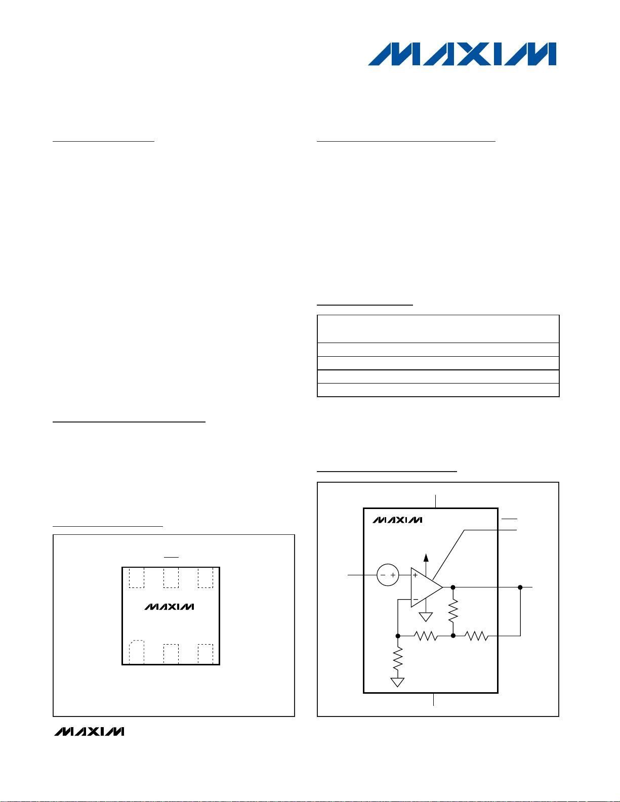
123
654
FB OUTSHDN
V
CC
INGND
MAX9504A
MAX9504B
µDFN
TOP VIEW
Pin Configurations
Ordering Information
MAX9504A
MAX9504B
IN
GND
1.2kΩ
2.3kΩ
580Ω 780Ω
OUT
FB
V
CC
SHDN
160mV OFFSET
MAX9504B
ONLY
Block Diagram
19-3750; Rev 0; 7/05
For pricing, delivery, and ordering information, please contact Maxim/Dallas Direct! at
1-888-629-4642, or visit Maxim’s website at www.maxim-ic.com.
Note: All devices specified over the -40°C to +85°C operating
range.
+Denotes lead-free package.
PART
PIN-
PKG
OFFSET
(mV)
TOP
MARK
MAX9504AELT-T
0
AAJ
MAX9504AEUT+T
0
ABWC
MAX9504BELT-T
160
AAK
MAX9504BEUT+
160
ABWD
Pin Configurations continued at end of data sheet.
PACKAGE
6 µDFN-6 L622-1
6 SOT23-6 U65-3
6 µDFN-6 L622-1
6 SOT23-6 U65-3
CODE
Page 2
MAX9504A/MAX9504B
3V/5V, 6dB Video Amplifiers with
High Output-Current Capability
2 _______________________________________________________________________________________
ABSOLUTE MAXIMUM RATINGS
DC ELECTRICAL CHARACTERISTICS
(VCC= 3.0V, GND = 0V, VIN= 0.5V, RL = infinity to GND, FB connected to OUT, SHDN = VCC, TA= -40°C to +85°C. Typical values
are at T
A
= +25°C, unless otherwise noted.) (Note 1)
Stresses beyond those listed under “Absolute Maximum Ratings” may cause permanent damage to the device. These are stress ratings only, and functional
operation of the device at these or any other conditions beyond those indicated in the operational sections of the specifications is not implied. Exposure to
absolute maximum rating conditions for extended periods may affect device reliability.
VCCto GND..............................................................-0.3V to +6V
IN, OUT, FB, SHDN to GND .......................-0.3V to (V
CC
+ 0.3V)
OUT Short-Circuit Duration to V
CC
or GND ..............Continuous
Continuous Power Dissipation (T
A
= +70°C)
6-Pin SOT23 (derate 8.7mW/°C above +70°C)............695mW
6-Pin µDFN (derate 4.7mW/°C above +70°C) .............377mW
Operating Temperature Range ..........................-40°C to +85°C
Junction Temperature .....................................................+150°C
Storage Temperature Range ............................-65°C to +150°C
Lead Temperature (soldering, 10s) ................................+300°C
PARAMETER
CONDITIONS MIN TYP MAX
UNITS
Supply Voltage Range V
CC
Guaranteed by PSRR 2.7 5.5 V
VCC = 3V 5 9
Quiescent Supply Current I
CC
VCC = 5V 5 9
mA
Shutdown Supply Current
SHDN = 0V 0.01 1 µA
MAX9504A 0.10 1.25
Input Voltage Range V
IN
Inferred from
voltage gain
MAX9504B 0 1.10
V
MAX9504A -25 0 +25
Input Offset Voltage V
OS
MAX9504B 120 160 200
mV
Input Bias Current I
BIAS
VIN = 0V 5 20 µA
Input Resistance R
IN
0 < V
IN
< 1.45V 4 MΩ
VCC = 2.7V,
0.1V < V
IN
< 1.10V
1.9 2.0 2.1
VCC = 3.0V,
0.1V < V
IN
< 1.25V
1.9 2.0 2.1
RL = 150Ω
(Note 2),
MAX9504A
V
CC
= 4.5V,
0.1V < V
IN
< 1.90V
2
VCC = 2.7V,
0 < V
IN
< 0.95V
1.9 2.0 2.1
VCC = 3.0V,
0 < V
IN
< 1.10V
1.9 2.0 2.1
Voltage Gain A
V
RL = 150Ω
(Note 2),
MAX9504B
V
CC
= 4.5V,
0 < V
IN
< 1.75V
2
V/V
MAX9504A 60 80
Power-Supply Rejection
Ratio
PSRR
MAX9504B 50 61
dB
Sourcing, RL = 20Ω to GND 45 85
Output Current I
OUT
Sinking, RL = 20Ω to V
CC
40 110
mA
Output Short-Circuit Current
I
SC
OUT shorted to VCC or GND 130 mA
SHDN Logic-Low Threshold
V
IL
V
SHDN Logic-High Threshold
V
IH
V
SHDN Input Current I
IN
SHDN = 0V or V
CC
0.003 1.000 µA
Shutdown Output
Impedance
R
OUT
(
)
SHDN = 0V 4 kΩ
SYMBOL
I
SHDN
Disabled
2.7V < VCC < 5.5V
VCC x 0.7
VCC x 0.3
Page 3
MAX9504A/MAX9504B
3V/5V, 6dB Video Amplifiers with
High Output-Current Capability
_______________________________________________________________________________________ 3
Note 1: All devices are 100% production tested at TA = +25°C. Specifications over temperature limits are guaranteed by design.
Note 2: Voltage gain (A
V
) is referenced to the input offset voltage; i.e., an input voltage of VINwould produce an output voltage of
V
OUT
= AVx (VIN+ VOS).
PARAMETER
CONDITIONS MIN TYP MAX
UNITS
Small-Signal -3dB
Bandwidth
BW
SS
V
OUT
= 100mV
P-P
47
MHz
Large-Signal -3dB
Bandwidth
BW
LS
V
OUT
= 2V
P-P
42
MHz
Small-Signal 0.1dB Gain
Flatness
V
OUT
= 100mV
P-P
10
MHz
Large-Signal 0.1dB Gain
Flatness
V
OUT
= 2V
P-P
12
MHz
Slew Rate SR V
OUT
= 2V step 165 V/µs
Settling Time to 1% t
S
V
OUT
= 2V step 25 ns
MAX9504A 75
Power-Supply Rejection
Ratio
PSRR f = 100kHz
MAX9504B 49
dB
Output Impedance Z
OUT
f = 5MHz 2.5 Ω
VCC = 3V 0.1
Differential Gain DG NTSC
V
CC
= 5V 0.1
%
VCC = 3V 0.3
Differential Phase DP NTSC
V
CC
= 5V 0.3
degrees
2T Pulse-to-Bar K Rating
2T = 250ns, bar time is 18µs, the beginning
2.5% and the ending 2.5% of the bar time
are ignored
0.2 K%
2T Pulse Response 2T = 250ns 0.1 K%
2T Bar Response
2T = 250ns, bar time is 18µs, the beginning
2.5% and the ending 2.5% of the bar time
are ignored
0.1 K%
Nonlinearity 5-step staircase 0.1 %
Group Delay Distortion D/dT f = 100kHz to 5.5MHz 2 ns
Peak Signal-to-RMS Noise
SNR VIN = 1V
P-P
, 100kHz < f < 5MHz 65 dB
Enable Time t
ON
V
I N
= 1V , V
OU T
settl ed to 1% of nom i nal
300 ns
Disable Time t
OFF
V
I N
= 1V , V
OU T
settl ed to 1% of nom i nal
85 ns
AC ELECTRICAL CHARACTERISTICS
(VCC= 3.0V, GND = 0V, VIN= 0.5V, RL= 150Ω to GND, FB connected to OUT, SHDN = VCC, TA= +25°C, unless otherwise noted.)
SYMBOL
BW
0.1dBSS
BW
0.1dBLS
Page 4
MAX9504A/MAX9504B
3V/5V, 6dB Video Amplifiers with
High Output-Current Capability
4 _______________________________________________________________________________________
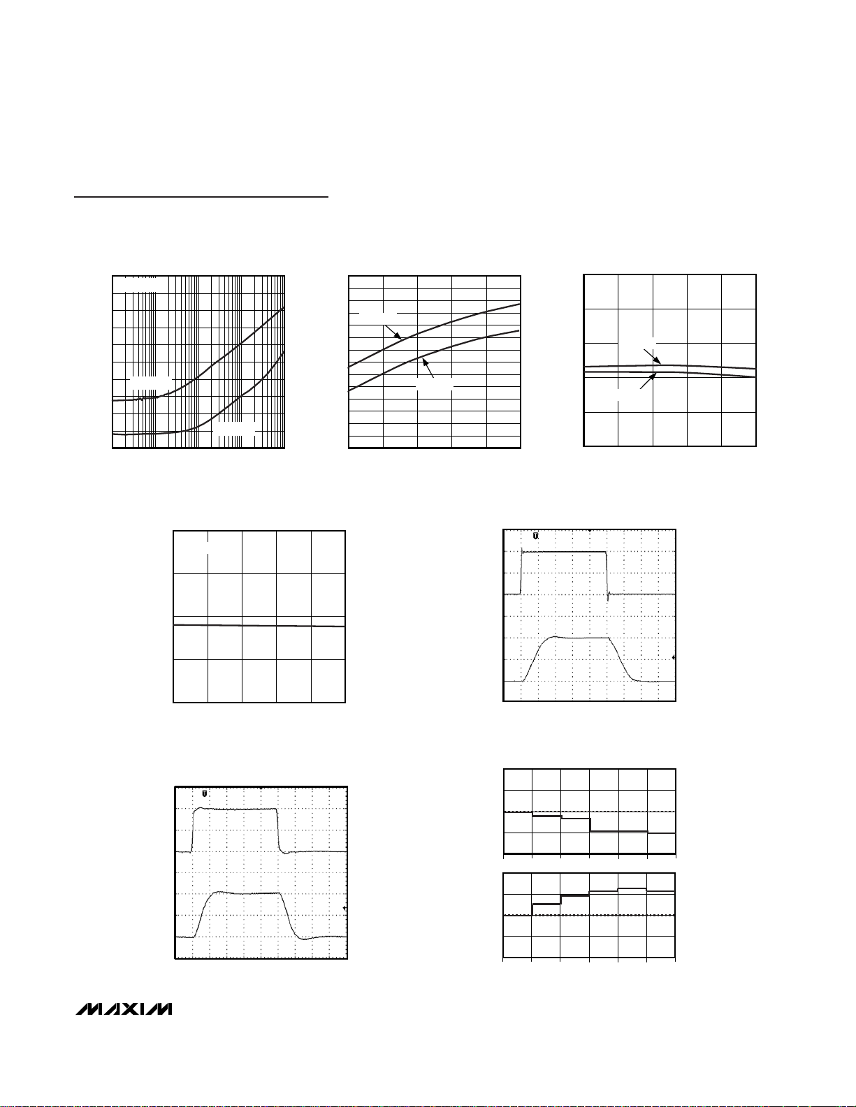
Typical Operating Characteristics
(VCC= 3.0V, GND = 0V, VIN= 0.5V, RL= 150Ω to GND, FB connected to OUT, SHDN = VCC, TA= +25°C, unless otherwise noted.)
SMALL-SIGNAL GAIN
vs. FREQUENCY
MAX9504 toc01
FREQUENCY (MHz)
GAIN (dB)
101
-5
-4
-3
-2
-1
0
1
2
3
-6
0.1 100
V
OUT
= 100mV
P-P
VCC = 3V
SMALL-SIGNAL GAIN FLATNESS
vs. FREQUENCY
MAX9504 toc02
FREQUENCY (MHz)
GAIN (dB)
101
-0.5
-0.4
-0.3
-0.2
-0.1
0
0.1
0.2
0.3
-0.6
0.1 100
V
OUT
= 100mV
P-P
VCC = 3V
SMALL-SIGNAL GAIN
vs. FREQUENCY
MAX9504 toc03
FREQUENCY (MHz)
GAIN (dB)
101
-5
-4
-3
-2
-1
0
1
2
3
-6
0.1 100
V
OUT
= 100mV
P-P
VCC = 5V
SMALL-SIGNAL GAIN FLATNESS
vs. FREQUENCY
MAX9504 toc04
FREQUENCY (MHz)
GAIN (dB)
101
-0.5
-0.4
-0.3
-0.2
-0.1
0
0.1
0.2
0.3
-0.6
0.1 100
V
OUT
= 100mV
P-P
VCC = 5V
LARGE-SIGNAL GAIN
vs. FREQUENCY
MAX9504 toc05
FREQUENCY (MHz)
GAIN (dB)
101
-5
-4
-3
-2
-1
0
1
2
3
4
-6
0.1 100
V
OUT
= 2V
P-P
VCC = 3V
LARGE-SIGNAL GAIN FLATNESS
vs. FREQUENCY
MAX9504 toc06
FREQUENCY (MHz)
GAIN (dB)
1010.1
-0.5
-0.4
-0.3
-0.2
-0.1
0
0.1
0.2
0.3
-0.6
0.01 100
V
OUT
= 2V
P-P
VCC = 3V
LARGE-SIGNAL GAIN
vs. FREQUENCY
MAX9504 toc07
FREQUENCY (MHz)
GAIN (dB)
101
-5
-4
-3
-2
-1
0
1
2
3
4
-6
0.1 100
V
OUT
= 2V
P-P
VCC = 5V
LARGE-SIGNAL GAIN FLATNESS
vs. FREQUENCY
MAX9504 toc08
FREQUENCY (MHz)
GAIN (dB)
101
-0.5
-0.4
-0.3
-0.2
-0.1
0
0.1
0.2
0.3
-0.6
0.1 100
V
OUT
= 2V
P-P
VCC = 5V
POWER-SUPPLY REJECTION RATIO
vs. FREQUENCY
MAX9504 toc09
FREQUENCY (MHz)
PSRR (dB)
10.10.01
-60
-50
-40
-30
-20
-10
0
10
-90
-80
-70
0.001 10
VCC = 3V
MAX9504B
MAX9504A
Page 5
MAX9504A/MAX9504B
3V/5V, 6dB Video Amplifiers with
High Output-Current Capability
_______________________________________________________________________________________ 5
POWER-SUPPLY REJECTION RATIO
vs. FREQUENCY
MAX9504 toc10
FREQUENCY (MHz)
PSRR (dB)
10.10.01
-60
-50
-40
-30
-20
-10
0
10
-90
-80
-70
0.001 10
VCC = 5V
MAX9504B
MAX9504A
QUIESCENT SUPPLY CURRENT
vs. TEMPERATURE
MAX9504 toc11
TEMPERATURE (°C)
SUPPLY CURRENT (mA)
603510-15
4.85
4.90
4.95
5.00
5.05
5.10
5.15
5.20
5.25
5.30
5.35
5.40
5.45
5.50
4.80
-40 85
VCC = 3V
VCC = 5V
MAX9504B INPUT OFFSET VOLTAGE
vs. TEMPERATURE
MAX9504 toc12
TEMPERATURE (°C)
V
OS
(V)
603510-15
0.15
0.16
0.17
0.18
0.19
0.14
-40 85
VCC = 3V
VCC = 5V
VOLTAGE GAIN
vs. TEMPERATURE
MAX9504 toc13
TEMPERATURE (°C)
GAIN (V/V)
603510-15
1.95
2.00
2.05
2.10
1.90
-40 85
VCC = 3V and 5V
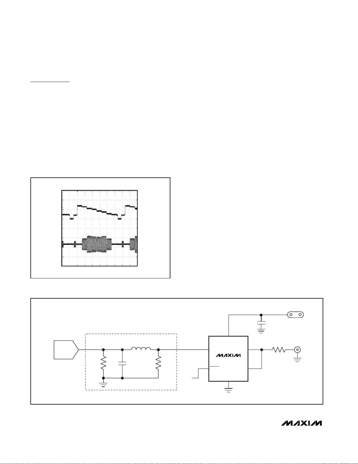
LARGE-SIGNAL STEP RESPONSE
MAX9504 toc14
10ns/div
V
IN
500mV/div
V
OUT
1V/div
SMALL-SIGNAL STEP RESPONSE
MAX9504 toc15
10ns/div
V
IN
25mV/div
V
OUT
50mV/div
DIFFERENTIAL GAIN AND PHASE
MAX9504 toc16
DIFFERENTIAL GAIN (%)
5432
-0.1
0
0.1
0.2
-0.2
16
DIFFERENTIAL PHASE (degrees)
5432
-0.2
0
0.2
0.4
-0.4
16
Typical Operating Characteristics (continued)
(VCC= 3.0V, GND = 0V, VIN= 0.5V, RL= 150Ω to GND, FB connected to OUT, SHDN = VCC, TA= +25°C, unless otherwise noted.)
Page 6

MAX9504A/MAX9504B
3V/5V, 6dB Video Amplifiers with
High Output-Current Capability
6 _______________________________________________________________________________________
Pin Description
PIN
SOT23
NAME FUNCTION
1 4 OUT Video Output
2 2 GND Ground
3 3 IN Video Input
41V
CC
Power-Supply Input. Bypass VCC with a 0.1µF capacitor to ground as close as possible to VCC.
55SHDN Shutdown Input. Pull SHDN low to place the device in low-power shutdown mode.
6 6 FB Feedback. Connect FB to OUT.
Typical Operating Characteristics (continued)
(VCC= 3.0V, GND = 0V, VIN= 0.5V, RL= 150Ω to GND, FB connected to OUT, SHDN = VCC, TA= +25°C, unless otherwise noted.)
OUT RESPONSE TO NTC-7
TEST SIGNAL (MAX9504B)
MAX9504 toc17
10µs/div
V
IN
500mV/div
GND
GND
V
OUT
1V/div
VCC = 3V
OUT RESPONSE TO NTC-7
TEST SIGNAL (MAX9504B)
MAX9504 toc18
10µs/div
V
IN
500mV/div
GND
GND
V
OUT
1V/div
VCC = 5V
GND
GND
OUT RESPONSE TO A FIELD
SQUARE WAVE (MAX9504B)
µDFN
MAX9504 toc19
VCC = 3V
2ms/div
V
IN
500mV/div
V
OUT
1V/div
GND
GND
OUT RESPONSE TO A FIELD
SQUARE WAVE (MAX9504B)
2ms/div
MAX9504 toc20
VCC = 5V
V
IN
500mV/div
V
OUT
1V/div
Page 7

Detailed Description
The MAX9504A/MAX9504B 3V/5V, 6dB video amplifiers
with low-power shutdown mode accept DC-coupled
inputs and drive up to two DC-coupled, 150Ω back-terminated video loads. The MAX9504B provides an internal input offset voltage of 160mV, which allows
DC-coupled input signals down to ground without clipping the output sync tip.
The MAX9504A/MAX9504B operate from a single +2.7V
to +5.5V supply and consume only 5mA of supply current. The low-power shutdown mode reduces supply current to less than 1µA, making the MAX9504A/MAX9504B
ideal for low-voltage, battery-powered video applications.
Output Current Capability
As shown in the Typical Application Circuit, the
MAX9504A/MAX9504B can drive up to two 150Ω loads
to ground at the same time because the outputs can
source guaranteed 45mA (min) current. Two 150Ω loads
to ground is the same as a single 75Ω load to ground.
Since the MAX9504A/MAX9504B can also sink guaranteed 40mA (min) current, they can also drive two, AC-coupled 150Ω loads. When VCC> 3V, the output can swing
2.4V
P-P
. When VCC> 4.5V, the output can swing 2.8V
P-P
.
Input Offset (MAX9504B)
The MAX9504A/MAX9504B amplify DC-coupled video
signals with a gain of +2V/V (+6dB). The MAX9504B
features a 160mV input offset voltage (VOS) that allows
a video signal input range to ground without clipping
the output sync tip. The MAX9504B output voltage is
the sum of the input voltage and the input offset voltage
gained up by a factor of 2.
V
OUT
= 2 x (VIN+ VOS)
For example, if VIN= 1V and VOS= 0.16V then:
V
OUT
= 2 x (1V + 0.16V) = 2.32V
Shutdown Mode
The MAX9504A/MAX9504B feature a low-power shutdown mode (I
SHDN
< 1µA) for battery-powered/
portable applications. Driving SHDN high enables the
output. Driving SHDN low disables the output and
places the MAX9504A/MAX9504B into a low-power
shutdown mode. In shutdown, the output resistance is
4kΩ (typ) due to the combination of feedback resistors
from OUT to ground with FB connected to OUT.
MAX9504A/MAX9504B
3V/5V, 6dB Video Amplifiers with
High Output-Current Capability
_______________________________________________________________________________________ 7
MAX9504A
MAX9504B
VIDEO
CURRENT
DAC
Z
0
= 75Ω
75Ω
75Ω
75Ω
R2
IN
GND
OUT
FB
V
CC
2.7V TO 5.5V
V
CC
SHDN
L1
C3
3-POLE RECONSTRUCTION LPF
160mV OFFSET
C2
0.1µF
R1
C1
Z0 = 75Ω
75Ω
MAX9504B
ONLY
Typical Application Circuit
Page 8
MAX9504A/MAX9504B
Applications Information
Using the MAX9504A/MAX9504B
with Video Current DACs
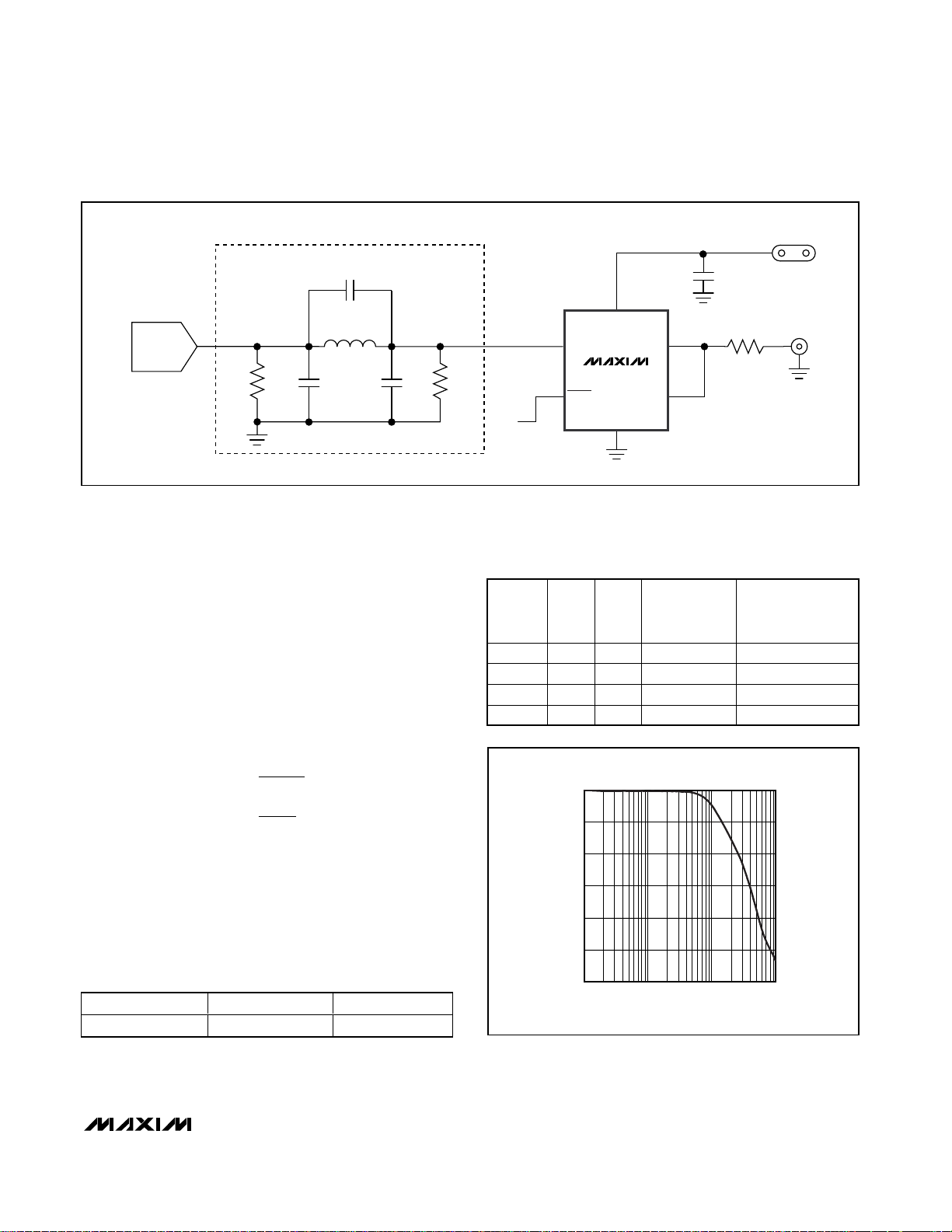
Video current DACs source current into a resistor connected to ground. The output voltage range for composite video and luma (Y) is usually from ground up to
1V (see Figure 1). Notice that the sync tip is quite close
to ground. Standard single-supply amplifiers with railto-rail outputs have difficulty amplifying input signals at
or near ground because their output stages enter a
nonlinear mode of operation when the output is pulled
close to ground.
The MAX9504B level shifts the input signal up by
160mV so that the output has a positive DC offset of
320mV. As a result, the MAX9504B output stage always
operates in the linear mode. Even if the input signal is
at ground, the MAX9504B output is at 320mV.
At the output of a video current DAC, the blank level of
the chroma signal is usually between 500mV to 650mV.
The voltage swing above and below the blank level is
approximately ±350mV (see Figure 1). If the blank level
is 550mV, then the lowest voltage for the chroma signal
is 200mV. For the case of chroma signals, no input
level shift is needed because 200mV gained up by two
is 400mV, which is well within the linear output range of
the MAX9504A or MAX9504B. Since the MAX9504A
does not have an input level shift, the MAX9504A
should be used with chroma signals. In summary, use
the MAX9504B with composite video and luma signals
from a DAC, and use the MAX9504A with chroma signals from a DAC.
Using the MAX9504A/MAX9504B with a
Video Reconstruction Filter
In most video applications, the video signal generated
from the DAC requires a reconstruction filter to smooth
out the steps and reduce the spikes. The MAX9504 has
a high-impedance, DC-coupled input that can be connected directly to the reconstruction filter.
For standard-definition video, the video passband is
approximately 6MHz, and the DAC sampling clock is
27MHz. Normally, a 9MHz lowpass filter can be used
for the reconstruction filter. This section demonstrates
the methods to build simple 2nd- and 3rd-order passive Butterworth lowpass filters with 9MHz cutoff frequency. See Figures 2 and 3.
3V/5V, 6dB Video Amplifiers with
High Output-Current Capability
8 _______________________________________________________________________________________
MAX9504 fig01
10µs/div
GND
LUMA
500mV/div
CHROMA
500mV/div
GND
Figure 1. Oscilloscope Trace of Luma and Chroma Signals
from Video Current DAC
R2
150Ω
R1
150Ω
C1
150pF
L1
3.9µH
R3
75Ω
C7
0.1µF
IN OUT
GND
FB
SHDN
V
CC
V
CC
V
CC
V
OUT
VIDEO
CURRENT
DAC
2-POLE RECONSTRUCTION LPF
MAX9504
Figure 2. 2nd-Order Butterworth LPF with MAX9504
Page 9
MAX9504A/MAX9504B
3V/5V, 6dB Video Amplifiers with
High Output-Current Capability
_______________________________________________________________________________________ 9
R2
150Ω
R1
150Ω
C1
120pF
C2
120pF
L1
4.7µH
C3
6.8pF
R3
75Ω
C7
0.1µF
IN OUT
GND
FB
SHDN
V
CC
V
CC
V
CC
V
OUT
VIDEO
CURRENT
DAC
3-POLE RECONSTRUCTION LPF
MAX9504
Figure 3. 3rd-Order Butterworth LPF with MAX9504
2nd-Order Butterworth Lowpass Filter Realization
Table 1 shows the normalized 2nd-order Butterworth
LPF component values at 1 rad/s with a source/load
impedance of 1Ω.
With the following equations, the L and C can be calculated for the cutoff frequency (fC) at 9MHz. Table 2
shows the appropriate L and C values for different
source/load impedances, the bench measurement values for the -3dB frequency and the attenuation at
27MHz. There is approximately 20dB attenuation at
27MHz, which decreases the spikes at the sampling
frequency.
Figure 4 shows the frequency response for R1 = R2 =
150Ω. At 6MHz, the attenuation is about 1.4dB. The
attenuation at 27MHz is about 20dB. Figure 5 shows
the multiburst response for R1 = R2 = 150Ω.
C
Cn
fcR
L
Ln R
fc
1
1
21
1
11
2
==
π
π
Table 1. 2nd-Order Butterworth Lowpass
Filter Normalized Values
Rn1 = Rn2 (Ω) Cn1 (F) Ln1 (H)
1 1.414 1.414
Table 2. Bench Measurement Values
(2nd-Order LPF)
R1 = R2
(Ω)
C1
3dB
FREQUENCY
(MHz)
ATTENUATION AT
27MHz (dB)
75
8.7 20
150
9.0 20
200
9.3 22
300
8.7 20
Figure 4. Frequency Response for 2nd-Order Lowpass Filter
(pF)L1(µH)
330 1.8
150 3.9
120 4.7
82 8.2
0
-10
-20
-30
GAIN (dB)
-40
-50
-60
FREQUENCY RESPONSE
0.1 1 10 100
FREQUENCY (MHz)
Page 10

MAX9504A/MAX9504B
3V/5V, 6dB Video Amplifiers with
High Output-Current Capability
10 ______________________________________________________________________________________
3rd-Order Butterworth Lowpass Filter Realization
If a flatter passband and more stopband attenuation
are desired, a 3rd-order lowpass filter can be used.
The design procedures are similar to the 2nd-order
Butterworth lowpass filter.
Table 3 shows the normalized 3rd-order Butterworth
lowpass filter with the cutoff frequency at 1 rad/s and
the stopband frequency at 3 rad/s. Table 4 shows the
appropriate L and C values for different source/load
impedances, the bench measurement values for the -3dB
frequency and the attenuation at 27MHz. The attenuation is over 40dB at 27MHz. At 6MHz, the attenuation is
approximately 0.6dB for R1 = R2 = 150Ω (Figure 6).
Y/C-to-Composite Mixer and Driver Circuit
The Y/C-to-composite mixer and driver use two lowpass filters, the MAX9504A and the MAX9504B. In
Figure 7, the top video DAC generates a luma signal,
which is filtered through the passive RLC network and
then amplified by the MAX9504B. The bottom video
DAC generates a chroma signal, which is filtered and
then amplified by the MAX9504A.
LUMA OUT is directly connected to the output of the
MAX9504B through a 75Ω back-termination resistor;
likewise, CHROMA OUT to the output of the MAX9504A.
CVBS OUT (the composite video with blanking and
sync output) is created by AC-coupling the chroma signal to the luma signal through the 470pF capacitor,
which looks like an AC short at the color subcarrier frequency of 3.58MHz for NTSC or 4.43MHz for PAL.
This circuit relies upon the feature that the MAX9504A/
MAX9504B can drive two loads at the same time.
Table 4. Bench Measurement Values—3rd Order LPF
R1 = R2 (Ω)
C1 (pF) C2 (pF) C3 (pF) L (µH)
3dB FREQUENCY (MHz)
ATTENUATION AT 27MHz (dB)
75 220 220 15.0 2.2 9.3 43
150 120 120 6.8 4.7 8.9 50
300 56 56 3.3 10.0 9.0 45
Table 3. 3rd-Order Butterworth Lowpass
Filter Normalized Values
Rn1 = Rn2
(Ω)
Cn1 (F)
Cn2 (F)
Cn3 (F)
Ln1 (H)
1 0.923 0.923 0.06 1.846
Figure 5. Multiburst Response
0.1 1 10 100
FREQUENCY RESPONSE
FREQUENCY (MHz)
GAIN (dB)
0
-60
-50
-40
-30
-20
-10
Figure 6. Frequency Response for 3rd-Order Lowpass Filter
V
IN
500mV/div
V
OUT
1V/div
10µs/div
Page 11

MAX9504A/MAX9504B
3V/5V, 6dB Video Amplifiers with
High Output-Current Capability
______________________________________________________________________________________ 11
150Ω
150Ω
120pF
120pF
4.7µH
6.8pF
75Ω
0.1µF
IN OUT
GND
FB
SHDN
V
CC
V
CC
LUMA OUT
VIDEO
CURRENT
DAC
LUMA
CHROMA
3-POLE RECONSTRUCTION LPF
MAX9504B
150Ω
150Ω
120pF
120pF
4.7µH
6.8pF
75Ω
470pF
0.1µF
IN OUT
GND
FB
SHDN
V
CC
VIDEO
CURRENT
DAC
3-POLE RECONSTRUCTION LPF
MAX9504A
75Ω
CHROMA OUT
75Ω
CVBS OUT
V
CC
Figure 7. Y/C-to-Composite Mixer and Driver Circuit
Page 12

MAX9504A/MAX9504B
3V/5V, 6dB Video Amplifiers with
High Output-Current Capability
12 ______________________________________________________________________________________
AC Output Coupling and Sag Correction
The MAX9504 can use the sag configuration if the output requires AC-coupling and VCC≥ 4.5V. Sag correction refers to the low-frequency compensation for the
highpass filter formed by the 150Ω load and the output
capacitor. In video applications, the cutoff frequency
must be less than 5Hz in order to pass the vertical sync
interval and avoid field time distortion (field tilt). In the
simplest configuration, a very large coupling capacitor
(> 220µF typically) is used to achieve the 5Hz cutoff
frequency. In the sag configuration, two smaller capacitors are used to replace the very large coupling capacitor (see Figure 8). For VCC≥ 4.5V, C5 and C6 are 22µF
capacitors.
Layout and Power-Supply Bypassing
The MAX9504A/MAX9504B operate from a single 2.7V
to 5.5V supply. Bypass the supply with a 0.1µF capacitor as close to VCCpossible. Maxim recommends using
microstrip and stripline techniques to obtain full bandwidth. To ensure that the PC board does not degrade
the device’s performance, design it for a frequency
greater than 1GHz. Pay careful attention to inputs and
outputs to avoid large parasitic capacitance. Whether
or not you use a constant-impedance board, observe
the following design guidelines:
• Do not use wire-wrap boards; they are too inductive.
• Do not use IC sockets; they increase parasitic capaci-
tance and inductance.
• Use surface-mount instead of through-hole components for better, high-frequency performance.
• Use a PC board with at least two layers; it should be
as free from voids as possible.
• Keep signal lines as short and as straight as possible.
Do not make 90° turns; round all corners.
R2
150Ω
R1
150Ω
C1
120pF
C2
120pF
L1
4.7µH
C3
6.8pF
R3
75Ω
C5
22µF
C6
22µF
C7
0.1µF
IN OUT
GND
FB
SHDN
V
CC
V
CC
V
CC
V
OUT
VIDEO
CURRENT
DAC
3-POLE RECONSTRUCTION LPF
MAX9504
Figure 8. SAG Correction Configuration
Page 13

MAX9504A/MAX9504B
3V/5V, 6dB Video Amplifiers with
High Output-Current Capability
______________________________________________________________________________________ 13
MAX9504A
MAX9504B
VIDEO
CURRENT
DAC
Z
0
= 75Ω
75Ω
75Ω
75Ω
R2
150Ω
IN
GND
1.2kΩ
2.3kΩ
580Ω 780Ω
OUT
FB
V
CC
2.7V TO 5.5V
V
CC
SHDN
L1
4.7µH
C3
6.8pF
3-POLE RECONSTRUCTION LPF
160mV OFFSET
C2
120pF
0.1µF
R1
150Ω
C1
120pF
Z0 = 75Ω
75Ω
MAX9504B
ONLY
Typical Operating Circuit
Chip Information
PROCESS: BiCMOS
GND
V
CC
IN
16FB
5 SHDN
OUT
+
MAX9504A
MAX9504B
SOT23-6
TOP VIEW
2
34
Pin Configurations (continued)
Page 14
MAX9504A/MAX9504B
3V/5V, 6dB Video Amplifiers with
High Output-Current Capability
14 ______________________________________________________________________________________
Package Information
(The package drawing(s) in this data sheet may not reflect the most current specifications. For the latest package outline information,
go to www.maxim-ic.com/packages
.)
6LSOT.EPS
Page 15

MAX9504A/MAX9504B
3V/5V, 6dB Video Amplifiers with
High Output-Current Capability
______________________________________________________________________________________ 15
Package Information (continued)
(The package drawing(s) in this data sheet may not reflect the most current specifications. For the latest package outline information,
go to www.maxim-ic.com/packages
.)
6, 8, 10L UDFN.EPS
EVEN TERMINAL
L
C
ODD TERMINAL
L
C
L
e
L
A
e
E
D
PIN 1
INDEX AREA
b
e
A
b
N
SOLDER
MASK
COVERAGE
A A
1
PIN 1
0.10x45∞
L
L1
(N/2 -1) x e)
XXXX
XXXX
XXXX
SAMPLE
MARKING
A1
A2
7
A
1
2
21-0164
PACKAGE OUTLINE,
6, 8, 10L uDFN, 2x2x0.80 mm
-DRAWING NOT TO SCALE-
Page 16

MAX9504A/MAX9504B
3V/5V, 6dB Video Amplifiers with
High Output-Current Capability
Maxim cannot assume responsibility for use of any circuitry other than circuitry entirely embodied in a Maxim product. No circuit patent licenses are
implied. Maxim reserves the right to change the circuitry and specifications without notice at any time.
16 ____________________Maxim Integrated Products, 120 San Gabriel Drive, Sunnyvale, CA 94086 408-737-7600
© 2005 Maxim Integrated Products Printed USA is a registered trademark of Maxim Integrated Products, Inc.
Package Information (continued)
(The package drawing(s) in this data sheet may not reflect the most current specifications. For the latest package outline information,
go to www.maxim-ic.com/packages
.)
COMMON DIMENSIONS
SYMBOL MIN. NOM.
A
0.70 0.75
A1
D 1.95 2.00
E
1.95 2.00
L
0.30 0.40
PKG. CODE N e b
PACKAGE VARIATIONS
L1
6L622-1 0.65 BSC 0.30±0.05
0.25±0.050.50 BSC8L822-1
0.20±0.030.40 BSC10L1022-1
2.05
0.80
MAX.
0.50
2.05
0.10 REF.
(N/2 -1) x e
1.60 REF.
1.50 REF.
1.30 REF.
A2
-
-DRAWING NOT TO SCALE-
A
2
2
21-0164
PACKAGE OUTLINE,
6, 8, 10L uDFN, 2x2x0.80 mm
0.15 0.20 0.25
0.020 0.025 0.035
 Loading...