

Page 1
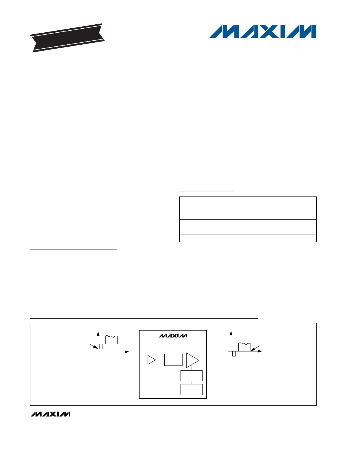
General Description
The MAX9503 filters and amplifies standard-definition
video signals. Maxim’s DirectDrive™ technology eliminates large output-coupling capacitors and sets the
video black level to ground. The input of the MAX9503
can be directly connected to the output of a video
digital-to-analog converter (DAC). The MAX9503 provides a compact, integrated, and low-power solution.
An internal reconstruction filter smoothes the steps and
reduces the spikes on the video signal from the DAC.
The reconstruction filter typically has 3dB attenuation at
9MHz and 50dB attenuation at 27MHz, and ±1dB passband flatness to 5.5MHz.
Maxim’s DirectDrive uses an integrated charge pump
and a linear regulator to create a clean negative power
supply to drive the sync below ground. The charge
pump injects so little noise into the video output that the
picture is visibly flawless.
The MAX9503 is available with +6dB (MAX9503G) and
+12dB (MAX9503M) gains. The device operates from a
2.7V to 3.6V single supply and features a 10nA lowpower shutdown mode.
The MAX9503 is offered in space-saving 16-pin QSOP
and 16-pin TQFN packages and is specified over the
-40°C to +85°C extended temperature range.
Applications
Digital Still Cameras
Mobile Phones/Smartphones
Security Cameras
Portable Media Players
Space-Constrained, Low-Power Portable
Devices
Features
♦ DC-Coupled Output
♦ Direct Connection to Video DAC
♦ Video Output Black Level Set to Ground
♦ Video Reconstruction Filter with 50dB
Attenuation at 27MHz
♦ Preset Gain
6dB (MAX9503G)
12dB (MAX9503M)
♦ 10nA Shutdown Supply Current
♦ 2.7V to 3.6V Single-Supply Operation
MAX9503
DirectDrive Video Amplifier with
Reconstruction Filter
________________________________________________________________ Maxim Integrated Products 1
Ordering Information
0 TO 50mV
0V
-0.1V TO
+0.1V
MAX9503
AMP
LINEAR
REGULATOR
CHARGE
PUMP
BUFFER
VIDOUT
VIDIN
MAX9503G: 6dB
MAX9503M: 12dB
LOWPASS
FILTER
0V
19-3676; Rev 1; 8/05
For pricing, delivery, and ordering information, please contact Maxim/Dallas Direct! at
1-888-629-4642, or visit Maxim’s website at www.maxim-ic.com.
EVALUATION KIT
AVAILABLE
PART*
PINPACKAGE
PKG CODE
TOP MARK
MAX9503GEEE
16 QSOP E16-4 —
MAX9503GETE
16 TQFN T1633-4 ACU
MAX9503MEEE
16 QSOP E16-4 —
MAX9503METE
16 TQFN T1633-4 ACV
Functional Diagram/Typical Operating Circuit and Pin
Configurations appear at end of data sheet.
*All devices are specified over the -40°C to +85°C operating
temperature range.
Block Diagram
Page 2
MAX9503
DirectDrive Video Amplifier with
Reconstruction Filter
2 _______________________________________________________________________________________
ABSOLUTE MAXIMUM RATINGS
ELECTRICAL CHARACTERISTICS
(VDD= CPVDD= SHDN = 3.0V, SGND = GND = CPGND = 0V, C1 = C2 = C3 = C4 = 1µF, R
BIAS
= 100kΩ, TA= T
MIN
to T
MAX
.
R
L
= 150Ω to SGND, unless otherwise noted. V
VIDIN
= 286mV (MAX9503G), V
VIDIN
= 143mV (MAX9503M). Typical values are at
V
DD
= CPV
DD
= SHDN = 3.0V, TA= +25°C, unless otherwise noted.) (Note 1)
Stresses beyond those listed under “Absolute Maximum Ratings” may cause permanent damage to the device. These are stress ratings only, and functional
operation of the device at these or any other conditions beyond those indicated in the operational sections of the specifications is not implied. Exposure to
absolute maximum rating conditions for extended periods may affect device reliability.
VDDto SGND............................................................-0.3V to +4V
VIDIN to SGND .........................................................-0.3V to +4V
BIAS to SGND ............................................-0.3V to (V
DD
+ 0.3V)
SHDN to SGND ........................................................-0.3V to +4V
VIDOUT to SGND........................(The greater of V
SS
and -2V) to
(V
DD
+ 0.3V)
CPV
DD
to CPGND ....................................................-0.3V to +4V
C1P, C1N, CPV
SS
.............................Capacitor Connection Only
CPGND, SGND, GND............................................-0.1V to +0.1V
CPV
SS
to V
SS ..................................................................
-0.1V to +0.1V
VIDOUT Short Circuit to V
DD
, SGND
and the Greater of (V
SS
and -2V) ...........................Continuous
Continuous Current
VIDIN, BIAS, SHDN ......................................................±20mA
Continuous Power Dissipation (T
A
= +70°C)
16-Pin QSOP (derate 8.3mW/°C above +70°C)...........667mW
16-Pin TQFN (derate 15.6mW/°C above +70°C) .......1349mW
Operating Temperature Range ...........................-40°C to +85°C
Junction Temperature......................................................+150°C
Storage Temperature Range .............................-65°C to +150°C
Lead Temperature (soldering, 10s) .................................+300°C
PARAMETER
CONDITIONS
Supply Voltage Range
V
DD
,
CPV
DD
Guaranteed by DC voltage gain and
quiescent current
2.7 3.6 V
Quiescent Supply Current I
DD
VDD = 3.6V (IDD = I
VDD
+ I
CPVDD
, RL = ∞) 1215mA
Shutdown Supply Current I
SHDN
VDD = 3.6V (I
SHDN
= I
VDD
+ I
CPVDD
),
SHDN = SGND
1µA
Bias Voltage V
BIAS
1V
VIDEO AMPLIFIER
MAX9503G
Guaranteed by DC
MAX9503M
MAX9503G
Input Voltage Range
Guaranteed by DC
voltage gain, V
DD
= 3V
MAX9503M
V
Input Current I
IN
VDD = 2.7V
µA
Input Resistance R
IN
1MΩ
MAX9503G 5.5 6 6.5
DC Voltage Gain (Note 2) A
V
VDD = 2.7V to 3.6V
MAX9503M
12
dB
MAX9503G
0
Output Black Level (Note 3) VDD = 2.7V
MAX9503M
0
V
Output Voltage Swing
V
P-P
Output Short-Circuit Current I
SC
Sinking or sourcing 50 mA
MAX9503G
Output Resistance R
OUT
MAX9503M
Ω
MAX9503G 4.2
Shutdown Output Impedance
SHDN = SGND
MAX9503M 8.2
kΩ
SYMBOL
MIN TYP MAX UNITS
V
RANGE
R
OUTSHDN
voltage gain, V
= 2.7V
DD
-0.10 +1.05
-0.050 +0.525
-0.10 +1.28
-0.05 +0.64
-2.5 +2.5
Guaranteed by DC voltage gain, VDD = 2.7V 2.162
11.5
-0.1
-0.15
Guaranteed by DC voltage gain, VDD = 3V 2.594
0.01
12.5
+0.1
+0.15
0.01
0.02
Page 3
MAX9503
DirectDrive Video Amplifier with
Reconstruction Filter
_______________________________________________________________________________________ 3
ELECTRICAL CHARACTERISTICS (continued)
(VDD= CPVDD= SHDN = 3.0V, SGND = GND = CPGND = 0V, C1 = C2 = C3 = C4 = 1µF, R
BIAS
= 100kΩ, TA= T
MIN
to T
MAX
.
R
L
= 150Ω to SGND, unless otherwise noted. V
VIDIN
= 286mV (MAX9503G), V
VIDIN
= 143mV (MAX9503M). Typical values are at
V
DD
= CPV
DD
= SHDN = 3.0V, TA= +25°C, unless otherwise noted.) (Note 1)
PARAMETER
SYMBOL
CONDITIONS
MIN
TYP
MAX
UNITS
CHARGE PUMP
Switching Frequency
300 kHz
LOGIC SIGNALS
Logic-Low Threshold V
IL
VDD = 2.7V to 3.6V 0.5 V
Logic-High Threshold V
IH
VDD = 2.7V to 3.6V 1.5 V
Logic Input Current I
IL
1µA
AC ELECTRICAL CHARACTERISTICS
(V
DD
= CPV
DD
= SHDN = 3.0V, SGND = GND = CPGND = 0V, C1 = C2 = C3 = C4 = 1µF, R
BIAS
= 100kΩ, TA= T
MIN
to T
MAX
. RL =
150Ω to SGND, unless otherwise noted. V
VIDIN
= 286mV (MAX9503G), V
VIDIN
= 143mV (MAX9503M). Typical values are at VDD=
CPV
DD
= SHDN = 3.0V, TA= +25°C, unless otherwise noted.) (Note 1)
PARAMETER
CONDITIONS
UNITS
Passband Flatness VDD = 2.7V, f = 100kHz to 5.5MHz -1 0 +1 dB
f = 9.1MHz 3
Attenuation
V
DD
= 2.7V,
VIDOUT= 2V
P-P
, attenuation
is referred to 100kHz
f = 27MHz 35 50
dB
MAX9503G 62
Power-Supply Rejection Ratio PSRR f = 100kHz
MAX9503M 56
dB
MAX9503G 0.5
Output Impedance Z
OUT
f = 5MHz
MAX9503M
Ω
MAX9503G 0.1
Differential Gain Error DG NTSC, VIDOUT = 2V
P-P
MAX9503M 0.1
%
MAX9503G 0.2
Differential Phase Error DP NTSC, VIDOUT = 2V
P-P
MAX9503M 0.2
D egr ees
2T Pulse-to-Bar K Rating
2T = 250ns, bar time is 18µs, the beginning
2.5% and the ending 2.5% of the bar time
are ignored
K%
2T Pulse Response 2T = 250ns 0.3 K%
2T Bar Response
2T = 250ns, bar time is 18µs, the beginning
2.5% and the ending 2.5% of the bar time
are ignored
0.7 K%
Nonlinearity 5-step staircase 0.2 %
Group-Delay Distortion D
Dt
100kHz to 5.5MHz 10 ns
VIDOUT Capacitive-Load Stability
C
L
V
OUT
= 2V
P-P
, no sustained oscillations 20 pF
SYMBOL
150 250
MIN TYP MAX
0.65
-0.3
Page 4
MAX9503
DirectDrive Video Amplifier with
Reconstruction Filter
4 _______________________________________________________________________________________
AC ELECTRICAL CHARACTERISTICS (continued)
(V
DD
= CPV
DD
= SHDN = 3.0V, SGND = GND = CPGND = 0V, C1 = C2 = C3 = C4 = 1µF, R
BIAS
= 100kΩ, TA= T
MIN
to T
MAX
. RL =
150Ω to SGND, unless otherwise noted. V
VIDIN
= 286mV (MAX9503G), V
VIDIN
= 143mV (MAX9503M). Typical values are at VDD=
CPV
DD
= SHDN = 3.0V, TA= +25°C, unless otherwise noted.) (Note 1)
PARAMETER
CONDITIONS
UNITS
MAX9503G 64
Peak Signal-to-RMS Noise SNR 100kHz to 5.5MHz
MAX9503M 58
dB
Enable Time t
ON
VIDIN = 0.5V, VIDOUT settled to within 1%
of the final voltage
0.2 ms
Disable Time t
OFF
VIDIN = 0.5V, VIDOUT settled to below 1%
of the output voltage
0.1 ms
Note 1: All devices are 100% production tested at TA= +25°C. Specifications over temperature are guaranteed by design.
Note 2: Voltage gain (A
V
) is a two-point measurement in which the output voltage swing is divided by the input voltage swing.
Note 3: With an output load attached, this offset will directly contribute to quiescent current.
MAX9503G
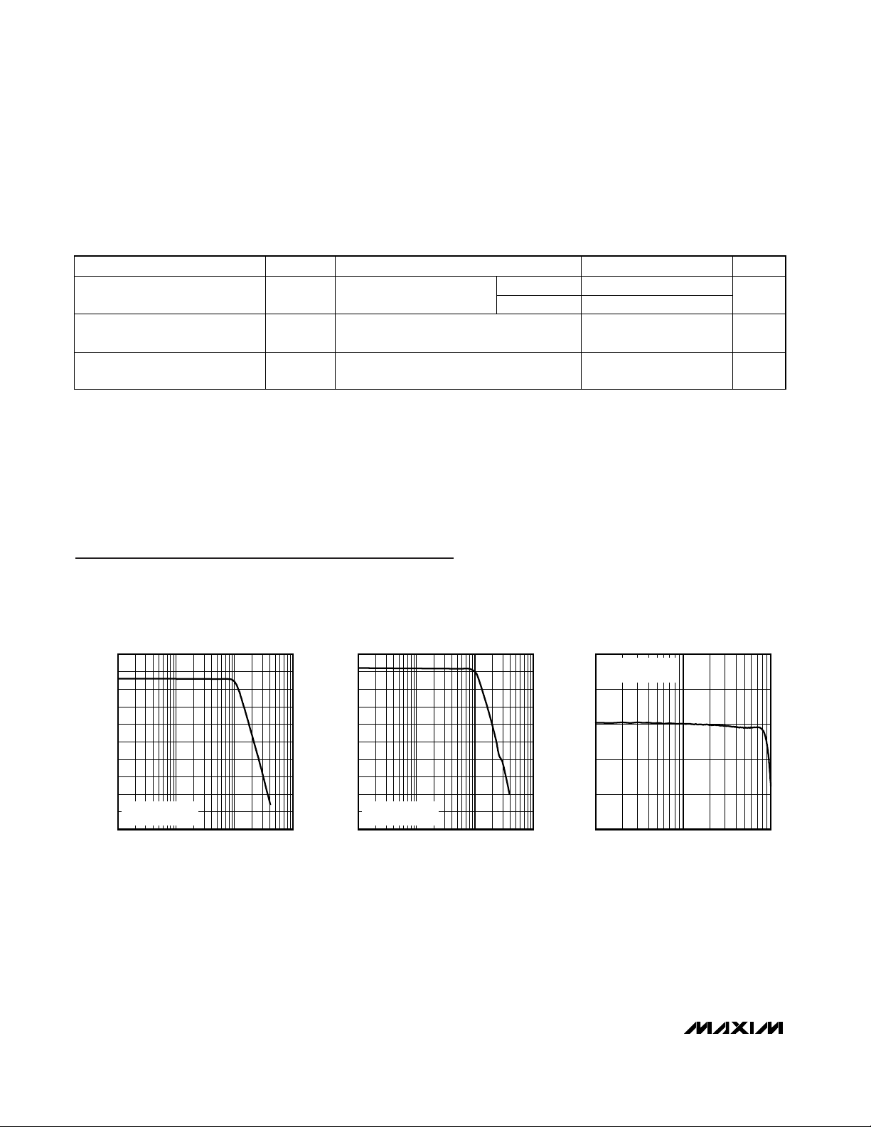
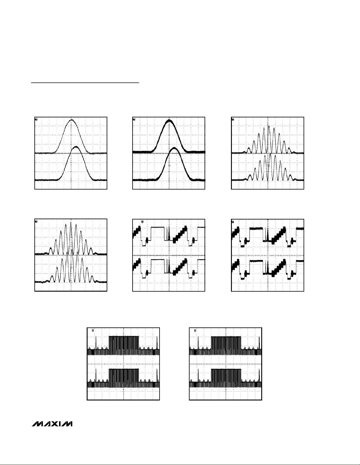
SMALL-SIGNAL GAIN vs. FREQUENCY
MAX9503 toc01
FREQUENCY (MHz)
GAIN (dB)
101
-70
-60
-50
-40
-30
-20
-10
0
10
20
-80
0.1 100
V
VIDOUT
= 100mV
P-P
GAIN = 6dB
MAX9503M
SMALL-SIGNAL GAIN vs. FREQUENCY
MAX9503 toc02
FREQUENCY (MHz)
GAIN (dB)
101
-70
-60
-50
-40
-30
-20
-10
0
10
20
-80
0.1 100
V
VIDOUT
= 100mV
P-P
GAIN = 12dB
MAX9503G SMALL-SIGNAL
GAIN FLATNESS vs. FREQUENCY
MAX9503 toc03
FREQUENCY (MHz)
GAIN FLATNESS (dB)
1
4
5
6
7
8
3
0.1 10
V
VIDOUT
= 100mV
P-P
GAIN = 6dB
Typical Operating Characteristics
(VDD= CPV
DD
= SHDN = 3.0V, SGND = GND = CPGND = 0V, no load, C1 = C2 = C3 = C4 = 1µF, R
BIAS
= 100kΩ, TA= T
MIN
to
T
MAX
. R
IN
= 150Ω to SGND, unless otherwise noted. V
VIDIN
= 286mV (MAX9503G), V
VIDIN
= 143mV (MAX9503M). Typical values
are at T
A
= +25°C, unless otherwise noted.)
SYMBOL
MIN TYP MAX
Page 5

MAX9503
DirectDrive Video Amplifier with
Reconstruction Filter
_______________________________________________________________________________________ 5
MAX9503M SMALL-SIGNAL
GAIN FLATNESS vs. FREQUENCY
MAX9503 toc04
FREQUENCY (MHz)
GAIN FLATNESS (dB)
1
10
11
13
12
14
15
9
0.1 10
V
VIDOUT
= 100mV
P-P
GAIN = 12dB
MAX9503G
LARGE-SIGNAL GAIN vs. FREQUENCY
MAX9503 toc05
FREQUENCY (MHz)
GAIN (dB)
101
-70
-60
-50
-40
-30
-20
-10
0
10
20
-80
0.1 100
V
VIDOUT
= 2V
P-P
GAIN = 6dB
MAX9503M
LARGE-SIGNAL GAIN vs. FREQUENCY
MAX9503 toc06
FREQUENCY (MHz)
GAIN (dB)
101
-70
-60
-50
-40
-30
-20
-10
0
10
20
-80
0.1 100
V
VIDOUT
= 2V
P-P
GAIN = 12dB
MAX9503G LARGE-SIGNAL
GAIN FLATNESS vs. FREQUENCY
MAX9503 toc07
FREQUENCY (MHz)
GAIN FLATNESS (dB)
1
4
5
6
7
8
3
0.1 10
V
VIDOUT
= 2V
P-P
GAIN = 6dB
MAX9503M LARGE-SIGNAL
GAIN FLATNESS vs. FREQUENCY
MAX9503 toc08
FREQUENCY (Hz)
GAIN FLATNESS (dB)
1
10
11
12
13
14
9
0.1 10
V
VIDOUT
= 2V
P-P
GAIN = 12dB
MAX9503G GROUP DELAY
MAX9503 toc09
FREQUENCY (MHz)
GROUP DELAY (ns)
101
25
50
75
100
125
150
0
0.1 100
V
VIDOUT
= 2V
P-P
MAX9503M GROUP DELAY
MAX9503 toc10
FREQUENCY (MHz)
GROUP DELAY (ns)
101
25
50
75
100
125
150
0
0.1 100
V
VIDOUT
= 2V
P-P
Typical Operating Characteristics (continued)
(VDD= CPV
DD
= SHDN = 3.0V, SGND = GND = CPGND = 0V, no load, C1 = C2 = C3 = C4 = 1µF, R
BIAS
= 100kΩ, TA= T
MIN
to
T
MAX
. R
IN
= 150Ω to SGND, unless otherwise noted. V
VIDIN
= 286mV (MAX9503G), V
VIDIN
= 143mV (MAX9503M). Typical values
are at T
A
= +25°C, unless otherwise noted.)
Page 6

MAX9503
DirectDrive Video Amplifier with
Reconstruction Filter
6 _______________________________________________________________________________________
Typical Operating Characteristics (continued)
(VDD= CPV
DD
= SHDN = 3.0V, SGND = GND = CPGND = 0V, no load, C1 = C2 = C3 = C4 = 1µF, R
BIAS
= 100kΩ, TA= T
MIN
to
T
MAX
. R
IN
= 150Ω to SGND, unless otherwise noted. V
VIDIN
= 286mV (MAX9503G), V
VIDIN
= 143mV (MAX9503M). Typical values
are at T
A
= +25°C, unless otherwise noted.)
MAX9503G POWER-SUPPLY
REJECTION RATIO vs. FREQUENCY
MAX9503 toc11
FREQUENCY (MHz)
PSRR (dB)
10.1
-100
-80
-60
-40
-20
0
20
-120
0.01 10
MAX9503M POWER-SUPPLY
REJECTION RATIO vs. FREQUENCY
MAX9503 toc12
FREQUENCY (MHz)
PSRR (dB)
10.1
-100
-80
-60
-40
-20
0
20
-120
0.01 10
QUIESCENT SUPPLY CURRENT
vs. TEMPERATURE
MAX9503 toc13
TEMPERATURE (°C)
SUPPLY CURRENT (mA)
603510-15
11
12
13
14
10
-40 85
MAX9503M
MAX9503G
MAX9503G VOLTAGE GAIN
vs. TEMPERATURE
MAX9503 toc14
TEMPERATURE (°C)
VOLTAGE GAIN (dB)
603510-15
5.9
6.0
6.1
6.2
5.8
-40 85
MAX9503M VOLTAGE GAIN
vs. TEMPERATURE
MAX9503 toc15
TEMPERATURE (°C)
VOLTAGE GAIN (dB)
603510-15
11.8
11.9
12.0
12.1
12.2
12.3
11.7
-40 85
MAX9503G OUTPUT VOLTAGE
vs. INPUT VOLTAGE
MAX9503 toc16
INPUT VOLTAGE (V)
OUTPUT VOLTAGE (V)
2.31.81.30.80.3
0
1
2
3
4
-1
-0.2 2.8
MAX9503M OUTPUT VOLTAGE
vs. INPUT VOLTAGE
MAX9503 toc17
INPUT VOLTAGE (V)
OUTPUT VOLTAGE (V)
0.8 1.00.60.40.20
-1
0
1
2
3
4
-2
-0.2 1.2
MAX9503G
DIFFERENTIAL GAIN AND PHASE
MAX9503 toc18
DIFFERENTIAL GAIN (%)
5432
0.2
0.1
-0.1
0
0.3
-0.3
16
DIFFERENTIAL PHASE (deg)
5432
0.2
0.1
-0.2
-0.1
0
0.3
-0.3
16
-0.2
MAX9503M
DIFFERENTIAL GAIN AND PHASE
MAX9503 toc19
DIFFERENTIAL GAIN (%)
5432
0.2
0.1
-0.1
0
0.3
-0.3
16
DIFFERENTIAL PHASE (deg)
5432
0.3
0.1
-0.3
-0.2
-0.1
0
0.4
-0.4
16
-0.2
0.2
Page 7
MAX9503
DirectDrive Video Amplifier with
Reconstruction Filter
_______________________________________________________________________________________ 7
MAX9503G 2T RESPONSE
MAX9503 toc20
VIDIN
200mV/div
VIDOUT
400mV/div
100ns/div
MAX9503M 2T RESPONSE
MAX9503 toc21
VIDIN
100mV/div
VIDOUT
400mV/div
100ns/div
MAX9503G 12.5T RESPONSE
MAX9503 toc22
VIDIN
250mV/div
VIDOUT
500mV/div
400ns/div
300mV
0V
MAX9503M 12.5T RESPONSE
MAX9503 toc23
VIDIN
100mV/div
VIDOUT
400mV/div
400ns/div
0V
150mV
MAX9503G OUT RESPONSE
TO NTC-7 VIDEO TEST SIGNAL
MAX9503 toc24
VIDIN
500mV/div
VIDOUT
1V/div
10μs/div
0V
0V
MAX9503M OUT RESPONSE
TO NTC-7 VIDEO TEST SIGNAL
MAX9503 toc25
VIDIN
250mV/div
VIDOUT
1V/div
10μs/div
0V
0V
MAX9503G OUT RESPONSE TO BLACK-
TO-WHITE VIDEO TEST SIGNAL
MAX9503 toc26
VIDIN
500mV/div
VIDOUT
1V/div
2ms/div
0V
0V
MAX9503M OUT RESPONSE TO BLACK-
TO-WHITE VIDEO TEST SIGNAL
MAX9503 toc27
VIDIN
250mV/div
VIDOUT
1V/div
2ms/div
0V
0V
Typical Operating Characteristics (continued)
(VDD= CPV
DD
= SHDN = 3.0V, SGND = GND = CPGND = 0V, no load, C1 = C2 = C3 = C4 = 1µF, R
BIAS
= 100kΩ, TA= T
MIN
to
T
MAX
. R
IN
= 150Ω to SGND, unless otherwise noted. V
VIDIN
= 286mV (MAX9503G), V
VIDIN
= 143mV (MAX9503M). Typical values
are at T
A
= +25°C, unless otherwise noted.)
Page 8

MAX9503
Detailed Description
The MAX9503 completely eliminates the need for
capacitors in the video output by using Maxim’s
DirectDrive technology that includes an inverting charge
pump and linear regulator. The charge pump and linear
regulator create a clean negative supply allowing the
amplifier output to swing below ground. The amplifier
output can swing both positive and negative so that the
video signal black level can be placed at ground. The
MAX9503 features a six-pole, Butterworth filter to perform reconstruction filtering on the video input signal
from the DAC.
DirectDrive
Background
Integrated video filter/amplifier circuits operating from a
single, positive supply usually create video output signals that are level-shifted above ground to keep the
signal within the linear range of the output amplifier. For
applications in which the positive DC level shift of the
video signal is not acceptable, a series capacitor can
be inserted in the output connection in an attempt to
eliminate the positive DC level shift. The series capacitor cannot truly level shift a video signal because the
average level of the video varies with picture content.
The series capacitor biases the video output signal
around ground, but the actual level of the video signal
can vary significantly depending upon the RC time constant and the picture content.
The series capacitor creates a highpass filter. Since
the lowest frequency in video is the frame rate, which
can be between 24Hz and 30Hz, the pole of the highpass filter should ideally be an order of magnitude
lower in frequency than the frame rate. Therefore, the
series capacitor must be very large, typically from
220µF to 3000µF. For space-constrained equipment,
the series capacitor is unacceptable. Changing from a
single series capacitor to a SAG network that requires
two smaller capacitors can only reduce space and
cost slightly.
The series capacitor in the usual output connection
also prevents damage to the output amplifier if the connector is shorted to a supply or to ground. While the
output connection of the MAX9503 does not have a
series capacitor, the MAX9503 will not be damaged if
the connector is shorted to a supply or to ground (see
the Short-Circuit Protection section).
Video Amplifier
Typically, the black level of the video signal created by
the video DAC is around 300mV. The MAX9503 shifts
the black level to ground at the output so that the active
video is above ground, and sync is below ground. The
amplifier needs a negative supply for its output stage to
remain in its linear region when driving sync below
ground.
DirectDrive Video Amplifier with
Reconstruction Filter
8 _______________________________________________________________________________________
Pin Description
PIN
QSOP TQFN
NAME
FUNCTION
115VSSNegative Power Supply. Connect to CPVSS.
216
Charge-Pump Negative Power Supply. Bypass with a 1µF capacitor to CPGND.
3 1 C1N
Charge-Pump Flying Capacitor Negative Terminal. Connect a 1µF capacitor from C1P to C1N.
42
Charge-Pump Power Ground
5 3 C1P Charge-Pump Flying Capacitor Positive Terminal. Connect a 1µF capacitor from C1P to C1N.
64
Charge-Pump Positive Power Supply. Bypass with a 1µF capacitor to CPGND.
7 5 BIAS Common-Mode Voltage. Connect a 100kΩ resistor from BIAS to SGND.
86
Signal Ground. Connect to GND.
9 7 VIDIN Video Input
10, 14, 15
N.C. No Connection. Not internally connected. Connect to SGND.
11 9 SHDN Active-Low Shutdown. Connect to VDD for normal operation.
12 10 GND Ground. Connect to SGND.
13 11 V
DD
Positive Power Supply. Bypass with a 1µF capacitor to SGND.
16 13
Video Output
— EP EP Exposed Paddle. Connect to GND.
CPV
SS
CPGND
CPV
DD
SGND
8, 12, 14
VIDOUT
Page 9
The MAX9503 has an integrated charge pump and linear
regulator to create a low-noise negative supply from the
positive supply voltage. The charge pump inverts the
positive supply to create a raw negative voltage that is
then fed into the linear regulator, which outputs -2V. The
linear regulator filters out the charge-pump noise.
Comparison Between DirectDrive Output
vs. AC-Coupled Output
The actual level of the video signal varies less with a
DirectDrive output than an AC-coupled output. The
video signal average can change greatly depending
upon the picture content. With an AC-coupled output,
the average will change according to the time constant
formed by the series capacitor and series resistance
(usually 150Ω). For example, Figure 1 shows an ACcoupled video signal alternating between a completely
black screen and a completely white screen. Notice the
excursion of the video signal as the screen changes.
With the DirectDrive amplifier, the black level is held at
ground. The video signal is constrained between
-0.3V to +0.7V. Figure 2 shows the video signal from a
DirectDrive amplifier with the same input signal as the
AC-coupled system.
Video Reconstruction Filter
Before the video signal from the DAC can be amplified,
it must be lowpass filtered to smooth the steps and to
reduce the spikes created whenever the DAC output
changes value. In the frequency domain, the steps and
spikes cause images of the video signal to appear at
multiples of the sampling clock. The MAX9503 contains
a six-pole Butterworth lowpass filter. The passband
extends to 5.5MHz, and the minimum attenuation is
35dB at 27MHz.
Short-Circuit Protection
The MAX9503 typical application circuit includes a 75Ω
back-termination resistor that limits short-circuit current if
an external short is applied to the video output. The
MAX9503 features internal output, short-circuit protection
to prevent device damage in prototyping and applications where the amplifier output can be directly shorted.
Shutdown
The MAX9503 features a low-power shutdown mode for
battery-powered/portable applications. Shutdown
reduces the quiescent current to less than 10nA.
Connecting SHDN to ground (SGND) disables the outputs and places the MAX9503 into a low-power shutdown mode. In shutdown mode, the amplifier, charge
pump, and linear regulator are turned off and the video
output impedance is 4kΩ.
MAX9503
DirectDrive Video Amplifier with
Reconstruction Filter
_______________________________________________________________________________________ 9
INPUT
500mV/div
OUTPUT
500mV/div
2ms/div
Figure 1. AC-Coupled Output
INPUT
500mV/div
OUTPUT
1V/div
2ms/div
0V
0V
Figure 2. DirectDrive Output
Page 10

MAX9503
Applications Information
Power-Supply Bypassing and Ground
Management
The MAX9503 operates from a 2.7V to 3.6V single supply and requires proper layout and bypassing. For the
best performance, place the components as close to
the device as possible.
Proper grounding improves performance and prevents
any switching noise from coupling into the video signal.
Connect GND and SGND together at a single point on
the PC board. Route all traces that carry switching tran-
sients away from SGND. Return SGND to the lowest
impedance ground available. Route CPGND and all
traces carrying switching transients away from SGND,
GND, and other traces and components in the video
signal path. Bypass the analog supply (VDD) with a 1µF
capacitor to SGND, placed as close to the device as
possible. Bypass the charge-pump supply (CPVDD)
with a 1µF capacitor to CPGND, placed as close to the
device as possible. Connect CPV
SS
to V
SS
and bypass
with a 1µF capacitor to CPGND as close to the device
as possible.
DirectDrive Video Amplifier with
Reconstruction Filter
10 ______________________________________________________________________________________
16
15
14
13
12
11
10
9
1
2
3
4
5
6
7
8
V
SS
VIDOUT
N.C.
N.C.
V
DD
GND
SHDN
N.C.
VIDIN
QSOP
CPV
SS
C1N
CPV
DD
CPGND
C1P
BIAS
SGND
MAX9503
12
13
14
15
16
8
7
6
5
11 10 9
1234
N.C.
VDDGND
SHDN
N.C.
VIDIN
SGND
BIAS
N.C.
V
SS
CPV
SS
C1N
CPGND
C1P
CPV
DD
VIDOUT
TOP VIEW
MAX9503
3mm x 3mm TQFN
Pin Configurations
Page 11

MAX9503
DirectDrive Video Amplifier with
Reconstruction Filter
______________________________________________________________________________________ 11
MAX9503G
(MAX9503M)
SHUTDOWN
CIRCUIT
LINEAR
REGULATOR
CHARGE PUMP
RECONSTRUCTION
FILTER
1V
AMP
BUFFER
V
DD
DC
LEVEL SHIFT
75Ω
75Ω
VIDOUT
6dB
(12dB)
CPGND C1P C1N CPV
SS
V
SS
C1
1μF
C2
1μF
100kΩ
BIAS
V
DD
1μF
C3
1μF
CPV
DD
V
DD
GND
SGND
VIDIN
SHDN
DAC
VIDEO
ASIC
Functional Diagram/Typical Operating Circuit
Chip Information
PROCESS: BiCMOS
Page 12

MAX9503
DirectDrive Video Amplifier with
Reconstruction Filter
12 ______________________________________________________________________________________
Package Information
(The package drawing(s) in this data sheet may not reflect the most current specifications. For the latest package outline information,
go to www.maxim-ic.com/packages
.)
QSOP.EPS
Page 13

MAX9503
DirectDrive Video Amplifier with
Reconstruction Filter
Maxim cannot assume responsibility for use of any circuitry other than circuitry entirely embodied in a Maxim product. No circuit patent licenses are
implied. Maxim reserves the right to change the circuitry and specifications without notice at any time.
Maxim Integrated Products, 120 San Gabriel Drive, Sunnyvale, CA 94086 408-737-7600 ____________________ 13
© 2005 Maxim Integrated Products Printed USA is a registered trademark of Maxim Integrated Products, Inc.
Package Information (continued)
(The package drawing(s) in this data sheet may not reflect the most current specifications. For the latest package outline information,
go to www.maxim-ic.com/packages
.)
MARKING
D/2
D
0.10 C 0.08 C
E/2
AAAA
E
(ND - 1) X e
C
L
C
L
C
A
A2
A1
L
L
e
(NE - 1) X e
D2/2
e
k
E2/2
L
E2
PACKAGE OUTLINE
8, 12, 16L THIN QFN, 3x3x0.8mm
e
b
C
L
21-0136
D2
0.10 M C A B
L
12x16L QFN THIN.EPS
1
I
2
8L 3x3
PKG
REF. MIN.
MIN.
NOM. MAX.
0.70 0.75 0.80
A
b
0.25 0.30 0.35
D
2.90
3.00 3.10
E
2.90 3.00 3.10
e
0.65 BSC.
L
0.35
0.55 0.75
ND
NE
0
0.02
A1
A2
0.20 REF
0.25
k
NOTES:
1. DIMENSIONING & TOLERANCING CONFORM TO ASME Y14.5M-1994.
2. ALL DIMENSIONS ARE IN MILLIMETERS. ANGLES ARE IN DEGREES.
3. N IS THE TOTAL NUMBER OF T ERMINALS.
4. THE TERMINAL #1 IDENTIFIER AND TERMINAL NUMBERING CONVENTION SHALL CONFORM TO
JESD 95-1 SPP-012. DETAILS OF TERMINAL #1 IDENTIFIER ARE OPTIONAL, BUT MUST BE LOCATED
WITHIN THE ZONE INDICATED. THE TERMINAL #1 IDENTIFIER MAY BE EITHER A MOLD OR
MARKED FEATURE.
5. DIMENSION b APPLIES TO METALLIZED TERMINAL AND IS MEASURED BETWEEN 0.20 mm AND 0.25 mm
FROM TERMINAL TIP.
6. ND AND NE REFER TO THE NUMBER OF TERMINALS ON EACH D AND E SIDE RESPECTIVELY.
7. DEPOPULATION IS POSSIBLE IN A SYMMETRICAL FASHION.
8. COPLANARITY APPLIES TO THE EXPOSED HEAT SINK SLUG AS WELL AS THE TERMINALS .
9. DRAWING CONFORMS TO JEDEC MO220 REVISION C.
10. MARKING IS FOR PACKAGE ORIENTATION REFERENCE ONLY.
11. NUMBER OF LEADS SHOWN ARE FOR REFERENCE ONLY.
12. WARPAGE NOT TO EXCEED 0.10mm.
12L 3x3
NOM. MAX. NOM.
0.70
0.75
0.20
0.25
2.90
3.00
2.90
3.00
0.50 BSC.
0.45
8
2
2
-
0.55
12N
0.05
0.0230.05
0
0.20 REF
-
0.25
3
-
0.80
0.30
3.10
3.10
0.65
-
16L 3x3
MIN. MAX.
0.70
0.75
0.20
0.25
2.90
3.00
2.90
3.00
0.50 BSC.
0.30
0.40
16
4
040.02
0.20 REF
-
0.25
EXPOSED PAD VARIATIONS
PKG.
0.80
0.30
3.10
3.10
0.50
0.05
CODES
TQ833-1 1.250.25 0.70 0.35 x 45° WEEC1.250.700.25
T1233-1
T1233-3
T1233-4
T1633-2 0.95
T1633F-3
T1633FH-3 0.65 0.80 0.95
T1633-4 0.95
T1633-5 0.95
-
D2
MIN.
NOM.
0.95
1.10
1.10
0.95
1.10
0.65
0.80
1.10 1.25 0.95 1.10
1.10
MAX.
E2
PIN ID
NOM.
MIN.
MAX.
1.25
1.10
0.95
1.25
1.251.10
1.25
0.95
1.25
1.25
0.95 1.10 0.35 x 45°1.25 WEED-10.95
1.100.95
1.10
1.25
0.95
0.80
0.95
0.65
0.95
0.65 0.80
1.25
1.10 1.25
0.95
PACKAGE OUTLINE
8, 12, 16L THIN QFN, 3x3x0.8mm
JEDEC
WEED-1
0.35 x 45°
WEED-11.25
0.35 x 45°
0.35 x 45°
WEED-2
0.225 x 45°
WEED-2
0.225 x 45°
WEED-2
0.35 x 45°
WEED-2
0.35 x 45° WEED-2
21-0136
2
I
2
 Loading...