

Page 1
General Description
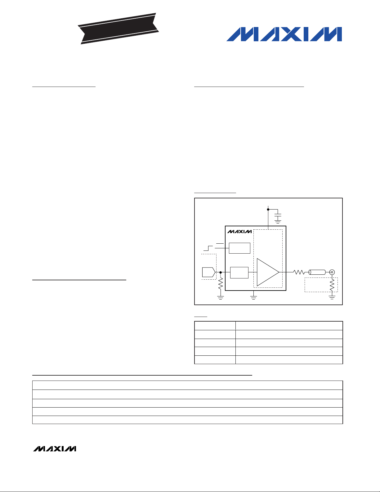
The MAX9502 small, low-power video amplifier with
integrated reconstruction filter operates from a supply
voltage as low as 2.5V. The small size and the low minimum supply voltage make the MAX9502 ideal for
portable applications or small, low-power applications.
The MAX9502 DC-couples the input and the output,
resulting in a very small solution. The MAX9502 input can
be directly connected to the output of a video digital-toanalog converter (DAC). The reconstruction filter is implemented as a 4th-order Chebyshev with a minimum
passband of 5.5MHz, 3dB attenuation at 8MHz, and
55dB attenuation at 27MHz.
The output amplifier provides a closed-loop gain of
+6dB (MAX9502G) or +12dB (MAX9502M), and can
drive a 2V
P-P
video signal into a 150Ω load to ground.
The output signal is level-shifted so the sync tip is
110mV (typ) above ground.
The MAX9502 operates from a 2.5V to 3.6V single supply
and consumes only 5.3mA quiescent supply current.
An active-low shutdown mode reduces the supply
current to 0.01µA.
The MAX9502 is available in tiny 6-pin µDFN (1mm x
1.5mm x 0.8mm) and 5-pin SC70 packages. The
device is specified over the -40°C to +85°C extended
and -40°C to +125°C automotive temperature ranges.
Applications
Mobile Phones
Digital Still Cameras
Portable Video
Automotive
Security/CCTV
Features
♦ Tiny 6-Pin µDFN (1mm x 1.5mm x 0.8mm) and
5-Pin SC70 Packages
♦ DC-Coupled Input and Output Save Board Space
♦ 4-Pole Chebyshev Filter
♦ 5.5MHz Passband
♦ 55dB Attenuation at 27MHz
♦ 0.01µA Low-Current Shutdown Mode
♦ 2.5V to 3.6V Single-Supply Operation
♦ Video Amplifier with Fixed Gains of +6dB
(MAX9502G) or +12dB (MAX9502M)
MAX9502
2.5V Video Amplifier with Reconstruction Filter
________________________________________________________________ Maxim Integrated Products 1
Ordering Information
19-3674; Rev 1; 6/06
For pricing, delivery, and ordering information, please contact Maxim/Dallas Direct! at
1-888-629-4642, or visit Maxim’s website at www.maxim-ic.com.
PART PIN-PACKAGE TEMP RANGE GAIN
TOP MARK
PKG CODE
MAX9502GAALT+T 6 µDFN-6 -40°C to +125°C +6 LI L611-1
MAX9502GAAXK+T 5 SC70-5 -40°C to +125°C +6 ASO X5-1
MAX9502GELT+T 6 µDFN-6 -40°C to +85°C +6 AU L611-1
MAX9502GEXK+T 5 SC70-5 -40°C to +85°C +6 ARV X5-1
Pin Configurations appear at end of data sheet.
Ordering Information continued at end of data sheet.
+Denotes lead-free package.
Other Portable Video Amplifiers
PRODUCT FEATURES
MAX9503 DirectDrive™, LPF, TQFN
MAX9505 DirectDrive, LPF, analog switch, TQFN
MAX4090 Input clamp, µDFN, SOT23, SC70
MAX9504 Optional DC offset bias, µDFN, SOT23
MAX9502
VIDEO AMP
GAIN = +6dB
MAX9502G
GAIN = +12dB
MAX9502M
SHUTDOWN
CIRCUIT
LOWPASS
FILTER
Z0 = 75Ω
75Ω
OUT
GND
75Ω TELEVISION
SHDN
IN
ON
OFF
VIDEO
DAC
VIDEO
ASIC
0.1µF
V
CC
Typical Operating Circuit
EVALUATION KIT
AVAILABLE
Page 2
MAX9502
2.5V Video Amplifier with Reconstruction Filter
2 _______________________________________________________________________________________
ABSOLUTE MAXIMUM RATINGS
DC ELECTRICAL CHARACTERISTICS
(VCC= SHDN = 3.0V, GND = 0V, no load, TA= T
MIN
to T
MAX
, unless otherwise noted. Typical values are at TA= +25°C, unless otherwise
noted.) (Note 1)
Stresses beyond those listed under “Absolute Maximum Ratings” may cause permanent damage to the device. These are stress ratings only, and functional
operation of the device at these or any other conditions beyond those indicated in the operational sections of the specifications is not implied. Exposure to
absolute maximum rating conditions for extended periods may affect device reliability.
VCCto GND..............................................................-0.3V to +4V
SHDN, IN, OUT to GND..............................-0.3V to (V
CC
+ 0.3V)
OUT Short-Circuit Duration to V
CC
, GND……............Continuous
Continuous Power Dissipation (T
A
= +70°C)
5-Pin SC70 (derate 3.1mW/°C above +70°C)……….. .247mW
6-Pin µDFN (derate 2.1mW/°C above +70°C)………...168mW
Operating Temperature Ranges:
MAX9502GE/ME ...............................................-40°C to +85°C
MAX9502GA/MA.............................................-40°C to +125°C
Junction Temperature......................................................+150°C
Storage Temperature Range .............................-65°C to +150°C
Lead Temperature (soldering, 10s) .................................+300°C
PARAMETER
SYMBOL
CONDITIONS
MIN
TYP
MAX
UNITS
Supply Voltage Range V
CC
Guaranteed by PSRR 2.5 3.6 V
,
TA = -40°C to +85°C
5.3 9
Quiescent Supply Current I
CC
,
TA = -40°C to +125°C
11
mA
Shutdown Supply Current I
SHDN
V
SHDN
= 0V
1µA
VCC = 2.5V 0
Guaranteed by DC
VCC = 3.0V 0 1.2
VCC = 2.5V 0
Input Voltage Range V
IN
Guaranteed by DC
VCC = 3.0V 0 0.6
V
Input Current I
IN
VIN = 0V 3.5 10 µA
Input Resistance R
IN
∆VIN/∆I
IN
17 MΩ
MAX9502G 5.5 6 6.5
DC Voltage Gain (Note 2) A
V
RL = 150Ω to GND,
V
CC
= 2.5V to 3V
MAX9502M
12
dB
Output Sync-Tip Level V
STIP
Measured at OUT, VIN = 0V,
R
L
= 150Ω to GND
mV
VCC = 2.5V,
2.1
MAX9502G,
R
L
= 150Ω to GND
V
CC
= 3.0V,
0 ≤ V
IN
≤ 1.2V
2.4
VCC = 2.5V,
2.1
Output Voltage Swing V
OUT
MAX9502M,
R
L
= 150Ω to GND
V
CC
= 3.0V,
0 ≤ V
IN
≤ 0.6V
2.4
V
P-P
Output Short-Circuit Current
Threshold
I
SC
Sourcing (Note 3) 95 mA
Output Resistance R
OUT
Ω
Shutdown Output Impedance
)
V
SHDN
= 0V 4 kΩ
DC Power-Supply Rejection Ratio
VIN = 0V, 2.5V ≤ VCC ≤ 3.6V 50 90 dB
LOGIC INPUTS (SHDN)
TA = -40°C to +85°C 0.8
Logic-Low Level V
IL
TA = -40°C to +125°C
V
Logic-High Level V
IH
2.0 V
Logic Input Current I
IL
SHDN = GND and V
CC
1µA
VIN = 0V, 2.5V ≤ VCC ≤ 3.6V, SHDN = V
VIN = 0V, 2.5V ≤ VCC ≤ 3.6V, SHDN = V
CC
CC
voltage gain (MAX9502G)
voltage gain (MAX9502M)
11.5
R
OUT(OFF
PSRR
DC
0 ≤ VIN ≤ 1.05V
1.97
2.26
1.97
0 ≤ VIN ≤ 0.525V
2.26
0.01
1.05
0.525
12.5
110 230
2.23
2.54
2.23
2.54
0.15
0.65
Page 3
MAX9502
2.5V Video Amplifier with Reconstruction Filter
_______________________________________________________________________________________ 3
PARAMETER
SYMBOL
CONDITIONS
MIN
TYP
MAX
UNITS
Passband Flatness
V
OUT
= 2V
P-P
, f = 100kHz to 5.5MHz,
flatness is referred to 100kHz
-1 +1 dB
f = 8MHz 3
Attenuation f
dt
V
OUT
= 2V
P-P
, attenuation is
referred to 100kHz
f = 27MHz 35 55
dB
Power-Supply Rejection Ratio PSRR f = 100kHz 56 dB
Output Impedance Z
OUT
V
OUT
= 1.5V DC; f = 5MHz 2.5 Ω
0.4
Differential Gain Error DG NTSC, V
OUT
= 2V
P-P
0.4
%
0.4
Differential Phase Error DP NTSC, V
OUT
= 2V
P-P
0.4
degrees
2T Pulse-to-Bar K Rating
2T = 250ns; bar time is 18µs; the beginning
2.5% and the ending 2.5% of the bar time
are ignored
0.2 K%
2T Pulse Response 2T = 250ns 0.3 K%
2T Bar Response
2T = 250ns; bar time is 18µs; the beginning
2.5% and the ending 2.5% of the bar time
are ignored
0.4 K%
Nonlinearity 5-step staircase 0.4 %
Line Time Distortion 0%
Field Time Distortion 0%
30
Group-Delay Variation
f = 100kHz to 5.5MHz
30
ns
68
Peak Signal to RMS Noise SNR
V
OUT
= 2V
P-P
, 100kHz to
5MHz
65
dB
MAX9502G
(V
IN
= 1V)
Enable Time t
ON
V
SHDN
= 3V, V
OUT
settled to
MAX9502M
ns
MAX9502G
(V
IN
= 1V)
Disable Time t
OFF
V
SHDN
= 0V, V
OUT
settled to
below 1% of the output
voltage
MAX9502M
ns
Note 1: All devices are 100% production tested at TA= +25°C. Specifications over temperature limits are guaranteed by design.
Note 2: DC voltage gain (A
V
) is a two-point measurement in which the output voltage swing is divided by the input voltage swing.
Note 3: Short-circuit current is the trip current for the protection. During the protection, OUT is switched alternatively on and off.
AC ELECTRICAL CHARACTERISTICS
(VCC= SHDN = 3.0V, GND = 0V, RL= 150Ω to GND, TA= +25°C, unless otherwise noted.) (Note 1)
MAX9502G
MAX9502M
MAX9502G
MAX9502M
∆(dϕ/dω)
within 1% of the final voltage
MAX9502G
MAX9502M
MAX9502G
MAX9502M
(V
= 0.5V)
IN
(VIN = 0.5V)
800
800
220
175
Page 4
MAX9502
2.5V Video Amplifier with Reconstruction Filter
4 _______________________________________________________________________________________
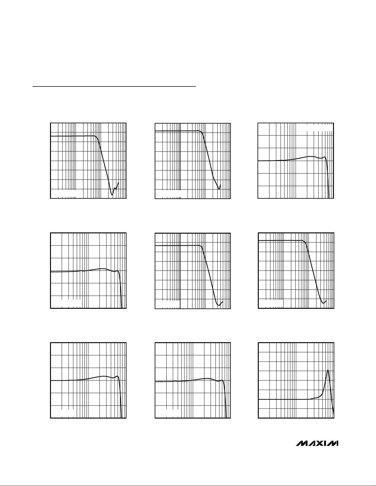
Typical Operating Characteristics
(VCC= SHDN = 3.0V, GND = 0V, RL= 150Ω to GND.)
MAX9502G
SMALL-SIGNAL BANDWIDTH
MAX9502 toc01
FREQUENCY (MHz)
RESPONSE (dB)
101
-50
-40
-30
-20
-10
0
10
20
-60
0.1 100
V
OUT
= 100mV
P-P
MAX9502M
SMALL-SIGNAL BANDWIDTH
MAX9502 toc02
FREQUENCY (MHz)
RESPONSE (dB)
101
-50
-40
-30
-20
-10
0
10
20
-60
0.1 100
V
OUT
= 100mV
P-P
MAX9502G
SMALL-SIGNAL GAIN FLATNESS
MAX9502 toc03
FREQUENCY (MHz)
RESPONSE (dB)
1
4
5
6
7
8
9
3
0.1 10
V
OUT
= 100mV
P-P
MAX9502M
SMALL-SIGNAL GAIN FLATNESS
MAX9502 toc04
FREQUENCY (MHz)
RESPONSE (dB)
1
10
11
12
13
14
15
9
0.1 10
V
OUT
= 100mV
P-P
MAX9502G
LARGE-SIGNAL BANDWIDTH
MAX9502 toc05
FREQUENCY (MHz)
RESPONSE (dB)
1010.1 100
V
OUT
= 2V
P-P
-50
-40
-30
-20
-10
0
10
20
-60
MAX9502M
LARGE-SIGNAL BANDWIDTH
MAX9502 toc06
FREQUENCY (MHz)
RESPONSE (dB)
101
-50
-40
-30
-20
-10
0
10
20
-60
0.1 100
V
OUT
= 2V
P-P
MAX9502G
LARGE-SIGNAL GAIN FLATNESS
MAX9502 toc07
FREQUENCY (MHz)
RESPONSE (dB)
1
4
5
6
7
8
9
3
0.1 10
V
OUT
= 2V
P-P
MAX9502M
LARGE-SIGNAL GAIN FLATNESS
MAX9502 toc08
FREQUENCY (MHz)
RESPONSE (dB)
1
10
11
12
13
14
15
9
0.1 10
V
OUT
= 2V
P-P
MAX9502G
GROUP DELAY
MAX9502 toc09
FREQUENCY (MHz)
DELAY (ns)
1
60
80
100
120
140
160
180
200
40
0.1 10
Page 5

MAX9502
2.5V Video Amplifier with Reconstruction Filter
_______________________________________________________________________________________ 5
MAX9502M
GROUP DELAY
MAX9502 toc10
FREQUENCY (MHz)
DELAY (ns)
1
60
80
100
120
140
160
180
200
40
0.1 10
MAX9502G
POWER-SUPPLY REJECTION RATIO
MAX9502 toc11
FREQUENCY (MHz)
RESPONSE (dB)
10.10.001 0.01
-90
-80
-70
-50
-60
-40
-30
-20
-10
0
-100
0.0001 10
MAX9502M
POWER-SUPPLY REJECTION RATIO
MAX9502 toc12
FREQUENCY (MHz)
RESPONSE (dB)
10.10.001 0.01
-90
-70
-80
-60
-50
-40
-30
-20
-10
0
-100
0.0001 10
SUPPLY CURRENT vs. TEMPERATURE
MAX9502 toc13
TEMPERATURE (°C)
SUPPLY CURRENT (mA)
6035-15 10
3.5
4.0
4.5
5.0
5.5
6.0
6.5
7.0
3.0
-40 85
MAX9502G
MAX9502M
SUPPLY CURRENT
vs. SHDN INPUT VOLTAGE
MAX9502 toc14
SHDN INPUT VOLTAGE (V)
SUPPLY CURRENT (mA)
2.52.01.51.00.5
0.5
1.0
1.5
2.0
2.5
3.0
3.5
4.0
4.5
5.0
5.5
6.0
0
0 3.0
V
SHDN
= RISING
SHUTDOWN LOGIC THRESHOLD
vs. SUPPLY VOLTAGE
MAX9502 toc15
SUPPLY VOLTAGE (V)
SHUTDOWN LOGIC THRESHOLD (V)
3.53.43.33.23.13.02.92.82.72.6
0.5
1.0
1.5
2.0
2.5
3.0
0
2.5 3.6
V
SHDN
= RISING
MAX9502G
VOLTAGE GAIN vs. TEMPERATURE
MAX9502 toc16
TEMPERATURE (°C)
GAIN (dB)
603510-15
5.7
5.9
6.1
6.3
6.5
5.5
-40 85
MAX9502M
VOLTAGE GAIN vs. TEMPERATURE
MAX9502 toc17
TEMPERATURE (°C)
GAIN (dB)
603510-15
11.7
11.9
12.1
12.3
12.5
11.5
-40 85
MAX9502G
DIFFERENTIAL GAIN AND PHASE
MAX9502 toc18
DIFFERENTIAL GAIN (%)
65432
0.2
0.1
-0.3
-0.1
0.4
-0.4
17
DIFFERENTIAL PHASE (deg)
65432
0.4
0
-0.4
0.8
-0.8
17
Typical Operating Characteristics (continued)
(VCC= SHDN = 3.0V, GND = 0V, RL= 150Ω to GND.)
Page 6

MAX9502
2.5V Video Amplifier with Reconstruction Filter
6 _______________________________________________________________________________________
Typical Operating Characteristics (continued)
(VCC= SHDN = 3.0V, GND = 0V, RL= 150Ω to GND.)
MAX9502M
DIFFERENTIAL GAIN AND PHASE
MAX9502 toc19
DIFFERENTIAL GAIN (%)
65432
0.2
0
-0.2
0.4
-0.4
17
DIFFERENTIAL PHASE (deg)
65432
0.4
0
-0.4
0.8
-0.8
17
MAX9502G
2T RESPONSE
MAX9502 toc20
IN
200mV/div
OUT
400mV/div
100ns/div
MAX9502M
2T RESPONSE
MAX9502 toc21
OUT
400mV/div
IN
100mV/div
100ns/div
MAX9502G
MODULATED 12.5T RESPONSE
MAX9502 toc22
IN
200mV/div
OUT
400mV/div
400ns/div
MAX9502M
MODULATED 12.5T RESPONSE
MAX9502 toc23
OUT
400mV/div
IN
100mV/div
400ns/div
MAX9502G
NTC-7 COMPOSITE RESPONSE
MAX9502 toc24
IN
500mV/div
0V
0V
OUT
1V/div
10µs/div
Page 7

MAX9502
2.5V Video Amplifier with Reconstruction Filter
_______________________________________________________________________________________ 7
MAX9502M
NTC-7 COMPOSITE RESPONSE
MAX9502 toc25
OUT
1V/div
IN
250mV/div
10µs/div
0V
0V
MAX9502G
MULTIBURST RESPONSE
MAX9502 toc26
OUT
1V/div
IN
500mV/div
10µs/div
0V
0V
MAX9502M
MULTIBURST RESPONSE
MAX9502 toc27
OUT
1V/div
IN
250mV/div
10µs/div
0V
0V
MAX9502G
FIELD SQUARE-WAVE RESPONSE
MAX9502 toc28
OUT
1V/div
IN
500mV/div
2ms/div
0V
0V
MAX9502M
FIELD SQUARE-WAVE RESPONSE
MAX9502 toc29
OUT
1V/div
IN
250mV/div
2ms/div
0V
0V
Typical Operating Characteristics (continued)
(VCC= SHDN = 3.0V, GND = 0V, RL= 150Ω to GND.)
Pin Description
PIN
µDFN SC70
NAME
FUNCTION
1 1 IN Video Input
2 2 GND Ground
33SHDN Active-Low Shutdown Input. Connect to GND to shutdown.
44VCCPositive Power Supply
5 — N.C. No Connection. Not internally connected.
6 5 OUT Video Output
Page 8

MAX9502
Detailed Description
The MAX9502 filters and amplifies the video DAC output
in applications such as digital still cameras and mobile
phones. The MAX9502 consists of a lowpass filter and an
output video buffer capable of driving a standard 150Ω
video load to ground. The MAX9502G output buffer provides a fixed gain of +6dB, while the MAX9502M output
buffer provides a fixed gain of +12dB.
Filter
The MAX9502 contains a 4th-order Chebyshev reconstruction filter. The Chebyshev-type response features
a 0.4dB flat passband for NTSC and PAL signals. The
stopband offers 55dB (typ) of attenuation at 27MHz
and above (see the Typical Operating Characteristics).
Output Amplifier
The MAX9502G features a +6dB gain, while the
MAX9502M features a +12dB gain. Operating from a
2.5V to 3.0V supply, the output amplifier is able to drive a
2V signal into a 150Ω video load to ground. Operating
from a 3.0V to 3.6V supply, the output amplifier is able to
drive a 2.4V
P-P
signal into a 150Ω video load to ground.
The output is typically offset 110mV above ground to
guarantee linear operation of the amplifier. The MAX9502
output only sources current; all loads should be connected to ground.
Short-Circuit Protection
The MAX9502 typical application circuit includes a 75Ω
back-termination resistor that limits short-circuit currents
for an external short applied at the video output. The
MAX9502 features internal output short-circuit protection
to prevent device damage in prototyping and applications where the amplifier output can be directly shorted.
Short-circuit protection activates if the output is short-circuited and the output current exceeds 95mA. During
short-circuit protection, the output of the MAX9502 is shut
off for 12µs and then turns on for 0.8µs. If the short is still
present, the MAX9502 output shuts off again. Extended
short circuits result in a pulsed output. The device
resumes normal operation after the short is removed.
Applications Information
Input Considerations
The MAX9502 input is DC-coupled. When the supply
voltage is between a 2.5V and 3V supply, the input voltage range extends from ground to 1.05V for the
MAX9502G and from ground to 0.525V for the
MAX9502M. When the supply voltage is between 3V and
3.6V, the input voltage range extends from ground to
1.2V for the MAX9502G and from ground to 0.6V for the
MAX9502M. The MAX9502G accepts a composite video
signal with a sync tip from 0 to 50mV and the MAX9502M
accepts a composite video signal with a sync tip from 0
to 25mV. A typical current-output DAC that operates
from a single supply usually creates a composite video
signal with a sync tip very close to ground. Hence, the
DAC output can be directly connected to the MAX9502
input. Keep the board trace as short as possible to minimize parasitic stray capacitance and prevent unintentional high-frequency attenuation.
Output Considerations
The MAX9502 output must be DC-coupled. No AC-coupling capacitors are allowed. The MAX9502 connects
directly to the video cable through a 75Ω series backtermination resistor. The other end of the cable should
be properly terminated with a 75Ω resistor as well.
Because of this configuration, the peak-to-peak amplitude as well as the DC level of the signal is divided by
two. The MAX9502 output signal is level-shifted up so
the sync tip is around 110mV.
Power-Supply Bypassing and Layout
Considerations
The MAX9502 operates from a single-supply voltage
down to 2.5V, allowing for low-power consumption.
Bypass VCCto GND with a 0.1µF capacitor. Place all
external components as close to the device as possible.
2.5V Video Amplifier with Reconstruction Filter
8 _______________________________________________________________________________________
Page 9

MAX9502
2.5V Video Amplifier with Reconstruction Filter
_______________________________________________________________________________________ 9
Chip Information
PROCESS: BICMOS
Ordering Information (continued)
PART PIN-PACKAGE TEMP RANGE GAIN
TOP MARK
PKG CODE
MAX9502MAALT+T 6 µDFN-6 -40°C to +125°C +12 LJ L611-1
MAX9502MAAXK+T 5 SC70-5 -40°C to +125°C +12 ASP X5-1
MAX9502MELT+T 6 µDFN-6 -40°C to +85°C +12 AV L611-1
MAX9502MEXK+T 5 SC70-5 -40°C to +85°C +12 ARW X5-1
Pin Configurations
TOP VIEW
SC70
GND
V
CC
SHDN
1 5 OUTIN
MAX9502
2
34
GND
V
CC
1
6
OUT5N.C.
IN
MAX9502
µDFN
23
4
SHDN
+Denotes lead-free package.
Page 10

MAX9502
2.5V Video Amplifier with Reconstruction Filter
10 ______________________________________________________________________________________
Package Information
(The package drawing(s) in this data sheet may not reflect the most current specifications. For the latest package outline information
go to www.maxim-ic.com/packages
.)
6L UDFN.EPS
-DRAWING NOT TO SCALE-
DOCUMENT CONTROL NO.APPROVAL
TITLE:
REV.
PACKAGE OUTLINE, 6L uDFN, 1.5x1.0x0.8mm
21-0147
2
2
D
2005 2006 2007 2008 2009 2010 2011 2012 2013 2014Calendar Year
Legend:
Marked with bar Blank space - no bar required
06-11Payweek 12-17 18-23 24-29 30-35 36-41 42-47 48-51 52-05
TABLE 2 Translation Table for Payweek Binary Coding
TABLE 1 Translation Table for Calendar Year Code
Legend: Marked with bar Blank space - no bar required
Page 11

MAX9502
2.5V Video Amplifier with Reconstruction Filter
Maxim cannot assume responsibility for use of any circuitry other than circuitry entirely embodied in a Maxim product. No circuit patent licenses are
implied. Maxim reserves the right to change the circuitry and specifications without notice at any time.
Maxim Integrated Products, 120 San Gabriel Drive, Sunnyvale, CA 94086 408-737-7600 ____________________ 11
© 2006 Maxim Integrated Products Printed USA is a registered trademark of Maxim Integrated Products, Inc.
Package Information (continued)
(The package drawing(s) in this data sheet may not reflect the most current specifications. For the latest package outline information,
go to www.maxim-ic.com/packages
.)
SC70, 5L.EPS
PACKAGE OUTLINE, 5L SC70
21-0076
1
E
1
 Loading...