

Page 1
General Description
The MAX9424–MAX9427 high-speed, low-skew quad
PECL-to-ECL translators are designed for high-speed
data and clock driver applications. These devices feature
an ultra-low 0.24ps
(RMS)
random jitter and channel-to-
channel skew is less than 90ps in asynchronous mode.
The four channels can be operated synchronously with
an external clock, or in asynchronous mode determined
by the state of the SEL input. An enable input provides
the ability to force all the outputs to a differential low state.
The parts differ from one another by their input and output termination options. The input options are an open
input or an internal differential 100Ω termination. The
output options are an open-emitter output or a series
50Ω termination. See Ordering Information.
The MAX9424–MAX9427 operate from a positive voltage
supply of +2.375V to +5.5V, and a negative supply voltage of -2.375V to -5.5V and operate across the extended
temperature range of -40°C to +85°C. They are offered in
32-pin 5mm x 5mm TQFP and space-saving 5mm x 5mm
QFN packages.
Applications
Data and Clock Driver and Buffer
Central Office Backplane Clock Distribution
DSLAM Backplane
Base Station
ATE
Features
♦ 0.24ps RMS Added Random Jitter
♦ 10ps Channel-to-Channel Skew in Synchronous
Mode
♦ Guaranteed 500mV Differential Output at 3GHz
Clock Frequency
♦ 420ps Propagation Delay in Asynchronous Mode
♦ Functionally Compatible with
SK4426 (MAX9424)
SK4430 (MAX9425)
SK4436 (MAX9426)
SK4440 (MAX9427)
♦ Integrated 50Ω Outputs (MAX9425/MAX9427)
♦ Integrated 100Ω Inputs (MAX9426/MAX9427)
♦ Synchronous/Asynchronous Operation
MAX9424–MAX9427
Lowest Jitter Quad PECL-to-ECL
Differential Translators
________________________________________________________________ Maxim Integrated Products 1
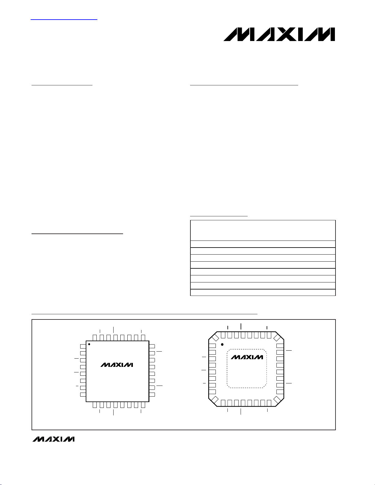
MAX9424
MAX9425
MAX9426
MAX9427
TQFP (5mm x 5mm)
TOP VIEW
32 28
293031
25
26
27
IN0
VGGOUT0
OUT0
IN0
VEEIN1
IN1
10
13
15
14
1611 12
9
IN3
V
GG
OUT3
IN2
V
EE
17
18
19
20
21
22
23
OUT1
24 V
GG
OUT1
V
EE
V
EE
OUT2
OUT2
V
GG
2
3
4
5
6
7
8V
CC
EN
CLK
SEL
1V
CC
SEL
CLK
EN
IN3
OUT3
IN2
32313029282726
IN0
IN0
V
GG
OUT0
OUT0
VEEIN1
25 IN1
9
1011121314
15
IN3
IN3
V
GG
OUT3
OUT3
V
EE
IN2
16
IN2
17
18
19
20
21
22
23
V
GG
NOTE: CORNER PINS ARE CONNECTED TO VGG.
OUT2
OUT2
V
EE
V
EE
OUT1
OUT1
8
7
6
5
4
3
2
V
CC
EN
EN
CLK
CLK
SEL
SEL
MAX9424
MAX9425
MAX9426
MAX9427
QFN
1V
CC
24 V
GG
TOP VIEW
*
*
*
*
Pin Configurations
Ordering Information
19-2390; Rev 0; 4/02
For pricing, delivery, and ordering information, please contact Maxim/Dallas Direct! at
1-888-629-4642, or visit Maxim’s website at www.maxim-ic.com.
*Future product—contact factory for availability.
PART
TEMP
RANGE
PIN-
OUTPUT
(OUT_,
OUT_)
MAX9424EHJ
32 TQFP
Open
MAX9424EGJ*
32 QFN
Open
MAX9425EHJ
32 TQFP
50Ω
MAX9425EGJ*
32 QFN
50Ω
MAX9426EHJ
32 TQFP
Open
MAX9426EGJ*
32 QFN
Open
MAX9427EHJ
32 TQFP
50Ω
MAX9427EGJ*
-40°C to +85°C
32 QFN
100Ω
50Ω
查询MAX9424供应商
PACKAGE
-40°C to +85°C
-40°C to +85°C
-40°C to +85°C
-40°C to +85°C
-40°C to +85°C
-40°C to +85°C
-40°C to +85°C
INPUT
(IN_,
IN_)
Open
Open
Open
Open
100Ω
100Ω
100Ω
Page 2
MAX9424–MAX9427
Lowest Jitter Quad PECL-to-ECL
Differential Translators
2 _______________________________________________________________________________________
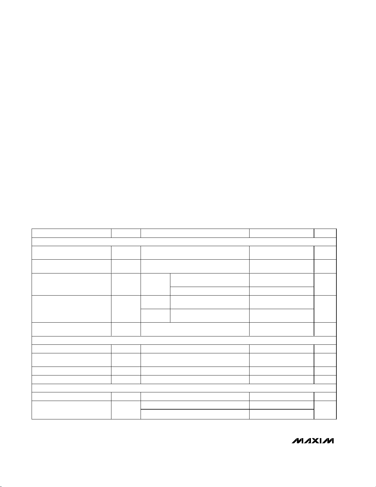
ABSOLUTE MAXIMUM RATINGS
DC ELECTRICAL CHARACTERISTICS
(VCC- VGG= 2.375V to 5.5V, VGG- VEE= 2.375V to 5.5V, MAX9424/MAX9426 outputs terminated with 50Ω to VGG- 2.0V,
MAX9425/MAX9427 not externally terminated, T
A
= -40°C to +85°C. Typical values are at VCC- VGG= 3.3V, VGG- VEE= 3.3V, V
IHD
= VCC- 0.9V, V
ILD
= VCC- 1.7V, TA= +25°C, unless otherwise noted.) (Notes 1, 2, and 3)
Stresses beyond those listed under “Absolute Maximum Ratings” may cause permanent damage to the device. These are stress ratings only, and functional
operation of the device at these or any other conditions beyond those indicated in the operational sections of the specifications is not implied. Exposure to
absolute maximum rating conditions for extended periods may affect device reliability.
VCCto VGG............................................................-0.3V to +6.0V
V
GG
to VEE.............................................................-0.3V to +6.0V
Input Pins to V
GG
........................................-0.3V to (V
CC
+ 0.3V)
Differential Input Voltage ..............................|V
CC
- VGG| or 3.0V,
whichever is less
Continuous Output Current .................................................50mA
Surge Output Current........................................................100mA
Continuous Power Dissipation (T
A
= +70°C)
32-Pin 5mm x 5mm TQFP
(derate 9.5mW/°C above +70°C).................................761mW
32-Pin 5mm x 5mm QFN
(derate 21.3mW/°C above +70°C)...................................1.7W
Junction-to-Ambient Thermal Resistance in Still Air
32-Pin 5mm x 5mm TQFP ........................................+105°C/W
32-Pin 5mm x 5mm QFN............................................+47°C/W
Junction-to-Ambient Thermal Resistance with
500LFPM Airflow
32-Pin 5mm x 5mm TQFP ..........................................+73°C/W
Junction-to-Case Thermal Resistance
32-Pin 5mm x 5mm TQFP ..........................................+25°C/W
32-Pin 5mm x 5mm QFN..............................................+2°C/W
Operating Temperature Range ...........................-40°C to +85°C
Junction Temperature......................................................+150°C
Storage Temperature Range .............................-65°C to +150°C
ESD Protection
Human Body Model (all input pins) ...............................±500V
Human Body Model (all output pins) ...............................±2kV
Soldering Temperature (10s) ...........................................+300°C
PARAMETER
CONDITIONS
UNITS
INPUTS (IN_, IN_, CLK, CLK, EN, EN, SEL, SEL)
Differential Input High Voltage V
IHD
Figure 1
V
GG
+
1.4
V
Differential Input Low Voltage V
ILD
Figure 1
VCC -
0.2
V
VCC - VGG < 3.0V 0.2
V
CC
-
Differential Input Voltage V
ID
Figure 1
V
CC
- VGG ≥ 3.0V 0.2 3.0
V
MAX9424/
EN, EN, SEL, SEL, IN_, IN_, CLK
or CLK = V
IHD
or V
ILD
-10 25
Input Current IIH, I
IL
MAX9426/
EN, EN, SEL, SEL, CLK, or CLK
= V
IHD
or V
ILD
-10 25
µA
Differential Input Resistance
(IN_, IN_)
R
IN
MAX9426/MAX9427 86
114 Ω
OUTPUTS (OUT_, OUT_)
Differential Output Voltage
Figure 1
mV
Output Common-Mode Voltage
V
OCM
Figure 1
V
GG
-
VGG -
VGG -
V
Output Impedance R
OUT
MAX9425/MAX9427 40 50 60 Ω
Internal Current Source I
SINK
MAX9425/MAX9427 6 8 10 mA
POWER SUPPLY
Positive Supply Current I
CC
(Note 4) 16 27 mA
MAX9424/MAX9426 (Note 4)
130
Negative Supply Current I
EE
MAX9425/MAX9427 (Note 4)
230
mA
SYMBOL
MIN TYP MAX
VOH - V
MAX9425
MAX9427
OL
V
GG
100
600 635
1.50
1.25
100
172
V
CC
V
GG
1.05
Page 3
MAX9424–MAX9427
Lowest Jitter Quad PECL-to-ECL
Differential Translators
_______________________________________________________________________________________ 3
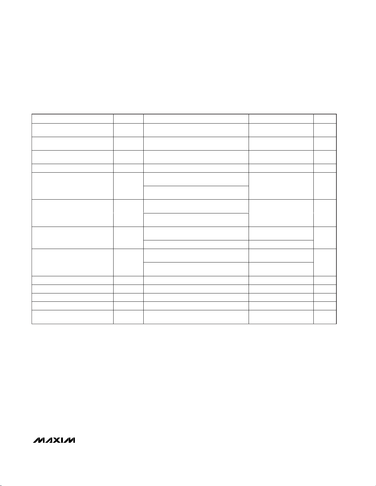
AC ELECTRICAL CHARACTERISTICS
(VCC- VGG= 2.375V to 5.5V, VGG- VEE= 2.375V to 5.5V, outputs terminated with 50Ω to VGG- 2.0V, EN = V
IHD
, EN = V
ILD
, f
CLK
≤
3.0GHz, f
IN
≤ 1.5GHz, input transition time = 125ps (20% to 80%), V
IHD
= VGG+ 1.4V to VCC, V
ILD
= VGGto VCC- 0.2V, V
IHD
- V
ILD
= 0.2V to smallest of |VCC- VGG| or 3.0V, TA= -40°C to +85°C, unless otherwise noted. Typical values are at VCC- VGG= 3.3V, V
GG
- VEE= 3.3V, V
IHD
= VCC- 0.9V, V
ILD
= VCC- 1.7V, TA= +25°C, unless otherwise noted.) (Notes 1 and 5)
PARAMETER
CONDITIONS
UNITS
IN_ to OUT_ Differential
Propagation Delay
t
PLH1
t
PHL1
Figure 3, SEL = high, asynchronous
operation
570 ps
CLK to OUT_ Differential
Propagation Delay
t
PLH2
t
PHL2
730 ps
OUT_ to OUT_ Skew t
SKD1
SEL = high, asynchronous operation
(Note 6)
38 90 ps
OUT_ to OUT_ Skew t
SKD2
10 70 ps
MAX9424/MAX9426, VOH - VOL ≥ 500mV,
SEL = low
Maximum Clock Frequency
)
MAX9425/MAX9427, VOH - VOL ≥ 300mV,
SEL = low
3.0 GHz
MAX9424/MAX9426, VOH - VOL ≥ 400mV,
SEL = high
Maximum Data Frequency
)
MAX9425/MAX9427, VOH - V
OL
≥ 250mV,
SEL = high
2.0 GHz
SEL = low, f
CLK
= 3.0GHz clock, fIN =
1.5GHz (Note 7)
0.8
Added Random Jitter t
RJ
SEL = high, fIN = 2.0GHz (Note 7) 0.3 0.8
ps
(RMS)
SEL = low, f
CLK
= 3.0GHz, IN_ = 3.0Gbps
2
23
- 1 PRBS pattern (Note 7)
27 80
Added Deterministic Jitter t
DJ
SEL = high, IN_ = 2.0Gbps 223 - 1 PRBS
pattern (Note 7)
20 80
ps
(P-P)
IN_ to CLK Setup Time t
S
Figure 4 80 ps
CLK to IN_ Hold Time t
H
Figure 4 80 ps
Output Rise Time t
R
Figure 3 89 120 ps
Output Fall Time t
F
Figure 3 87 120 ps
Propagation Delay Temperature
Coefficient
0.2 1
ps/°C
Note 1: Measurements are made with the device in thermal equilibrium.
Note 2: Current into a pin is defined as positive. Current out of a pin is defined as negative.
Note 3: DC parameters are production tested at +25°C. DC limits are guaranteed by design and characterization over the full
operating temperature range.
Note 4: All outputs open, all inputs biased differential high or low except V
CC
, VGG, and VEE.
Note 5: Guaranteed by design and characterization, and are not production tested. Limits are set to ±6 sigma.
Note 6: Measured between outputs of the same part at the signal crossing points for a same-edge transition.
Note 7: Device jitter added to the input signal.
SYMBOL
MIN TYP MAX
300 420
Figure 4, SEL = low, synchronous operation 460 580
SEL = low, synchronous operation (Note 6)
f
CLK(MAX
f
IN(MAX
0.24
∆tPD/∆T
Page 4
MAX9424–MAX9427
Lowest Jitter Quad PECL-to-ECL
Differential Translators
4 _______________________________________________________________________________________
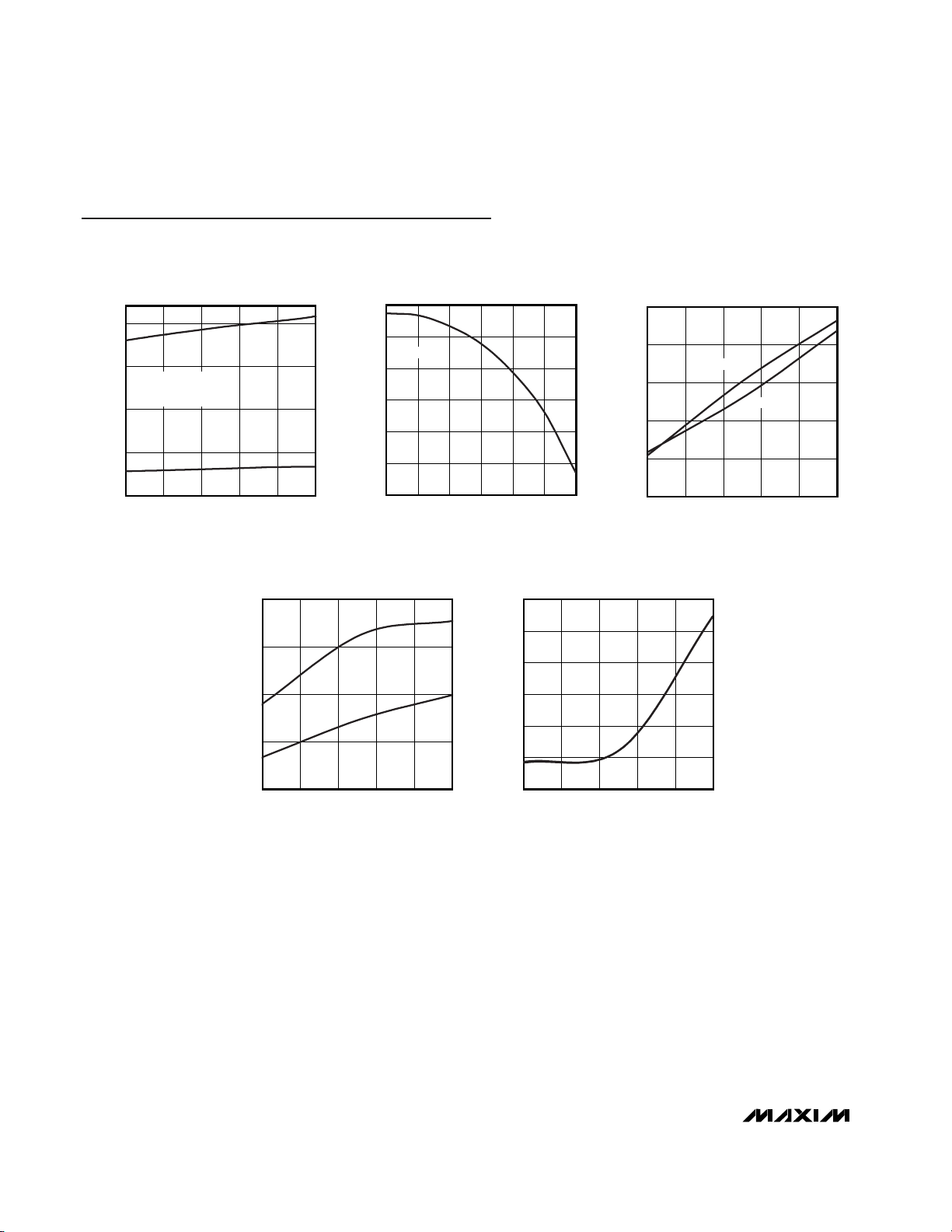
Typical Operating Characteristics
(MAX9424: VCC- VGG= 3.3V, VGG- VEE= 3.3V, outputs terminated with 50Ω to VGG- 2.0V, enabled, f
CLK
= 3.0GHz, fIN= 1.5GHz,
input transition time = 125ps (20% to 80%), V
IHD
= VCC- 0.9V, V
ILD
= VCC- 1.7V, TA= +25°C, unless otherwise noted.)
SUPPLY CURRENT vs. TEMPERATURE
MAX9424–MAX9427 toc01
TEMPERATURE (°C)
SUPPLY CURRENT (mA)
603510-15
25
50
75
100
0
-40 85
I
EE
I
CC
INPUTS BIASED
DIFFERENTIALLY HIGH OR
LOW, OUTPUTS OPEN
OUTPUT AMPLITUDE (VOH - VOL)
vs. IN_ FREQUENCY
MAX9424–MAX9427 toc02
IN_ FREQUENCY (GHz)
OUTPUT AMPLITUDE (mV)
2.52.01.51.00.5
400
450
500
550
600
650
350
03.0
SEL = HIGH
OUTPUT RISE/FALL TIME
vs. TEMPERATURE
MAX9424–MAX9427 toc03
TEMPERATURE (°C)
OUTPUT RISE/FALL TIME (ps)
603510-15
86
88
90
92
94
84
-40 85
RISE TIME
FALL TIME
IN-TO-OUT PROPAGATION DELAY
vs. TEMPERATURE
MAX9424–MAX9427 toc04
TEMPERATURE (°C)
IN-TO-OUT PROPAGATION DELAY (ps)
603510-15
390
400
410
420
380
-40 85
t
PHL1
t
PLH1
CLK-TO-OUT PROPAGATION DELAY
vs. TEMPERATURE
MAX9424–MAX9427 toc05
TEMPERATURE (°C)
CLK-TO-OUT PROPAGATION DELAY (ps)
603510-15
580
590
600
610
620
630
570
-40 85
t
PLH2
,
t
PHL2
Page 5

MAX9424–MAX9427
Lowest Jitter Quad PECL-to-ECL
Differential Translators
_______________________________________________________________________________________ 5
Pin Description
PIN NAME FUNCTION
1, 8 V
CC
Positive Supply Voltage. Bypass VCC to VGG with 0.1µF and 0.01µF ceramic capacitors. Place the
capacitors as close to the device as possible with the smaller value capacitor closest to the device.
2 SEL
Noninverting Differential Select Input. Setting SEL = 1 and SEL = 0 enables all four channels to
operate independently. Setting SEL = 0 and SEL = 1 enables all four channels to be synchronized to
CLK.
3 SEL Inverting Differential Select Input
4 CLK Noninverting Differential Clock Input
5 CLK Inverting Differential Clock Input
6EN
Noninverting Differential Output Enable Input. Setting EN = 1 and EN = 0 enables all four outputs.
Setting EN = 0 and EN = 1 disables all four outputs.
7 EN Inverting Differential Output Enable Input
9 IN3 Noninverting Differential Input 3
10 IN3 Inverting Differential Input 3
11, 17, 24,
30
V
GG
Ground Reference
12 OUT3 Inverting Differential Output 3
13 OUT3 Noninverting Differential Output 3
14, 20, 21,
27
V
EE
Negative Supply Voltage. Bypass from VEE to VGG with 0.1µF and 0.01µF ceramic capacitors. Place
the capacitors as close to the device as possible with the smaller value capacitor closest to the
device.
15 IN2 Noninverting Differential Input 2
16 IN2 Inverting Differential Input 2
18 OUT2 Inverting Differential Output 2
19 OUT2 Noninverting Differential Output 2
22 OUT1 Noninverting Differential Output 1
23 OUT1 Inverting Differential Output 1
25 IN1 Inverting Differential Input 1
26 IN1 Noninverting Differential Input 1
28 OUT0 Noninverting Differential Output 0
29 OUT0 Inverting Differential Output 0
31 IN0 Inverting Differential Input 0
32 IN0 Noninverting Differential Input 0
Page 6
MAX9424–MAX9427
Lowest Jitter Quad PECL-to-ECL
Differential Translators
6 _______________________________________________________________________________________
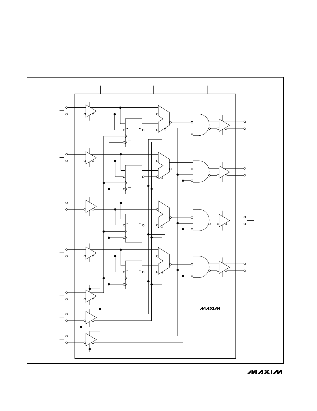
Functional Diagram
D
V
CC
V
CC
V
EE
V
GG
V
CC
V
EE
V
CC
V
EE
V
CC
V
EE
V
CC
V
EE
V
GG
V
CC
V
GG
V
CC
V
GG
V
CC
V
CC
V
GG
V
GG
Q
CK
D
Q
CK
1
28
29
32
1, 8
11, 17,
24, 30
14, 20,
21, 27
31
26
25
15
16
9
10
4
5
2
3
6
7
22
23
19
18
13
12
0
IN0
IN0
OUT0
OUT0
DQ
CK
D
Q
CK
1
0
IN1
IN1
OUT1
OUT1
DQ
CK
D
Q
CK
1
0
IN2
IN2
OUT2
OUT2
DQ
CK
D
Q
CK
1
0
IN3
IN3
CLK
CLK
SEL
SEL
EN
EN
OUT3
OUT3
MAX9424
MAX9425
MAX9426
MAX9427
Page 7

Detailed Description
The MAX9424–MAX9427 high-speed, low-skew PECL-toECL differential translators are designed for high-speed
data and clock driver applications. These devices translate up to four PECL signals to ECL signals.
The four channels can be operated synchronously with
an external clock, or in asynchronous mode, determined
by the state of the SEL input. An enable input provides
the ability to force all the outputs to a differential low state.
A variety of input and output terminations are offered
for maximum design flexibility. The MAX9424 has open
inputs and open-emitter outputs. The MAX9425 has
open inputs and 50Ω series outputs. The MAX9426 has
100Ω differential input impedance and open-emitter
outputs. The MAX9427 has 100Ω differential input
impedance and 50Ω series outputs.
Supply Voltages
These devices require a positive voltage supply (connect to VCC), a negative voltage supply (connect to
VEE), and a ground reference (connect to VGG). VCCis
independent of VEEand therefore the supply voltages
do not need to be symmetrical. The PECL input voltages are referenced to VCC, and the ECL output voltages are referenced to VGG.
Data Inputs and Outputs
The input and output structures are shown in Figure 2.
The open inputs of the MAX9424/MAX9425 require
external termination, whereas the MAX9426/MAX9427
have integrated 100Ω differential input termination
resistors between IN_ and IN_.
MAX9424–MAX9427
Lowest Jitter Quad PECL-to-ECL
Differential Translators
_______________________________________________________________________________________ 7
V
CC
V
ID
V
ID
= 0
V
IHD
(MAX) V
GG
V
EE
V
ILD
(MAX)
V
OH
- V
OL
V
OCM
V
OH
V
OL
V
GG
V
ID
V
ID
= 0
V
IHD
(MIN)
V
ILD
(MIN)
INPUT VOLTAGE DEFINITION
(PECL)
OUTPUT VOLTAGE DEFINITION
(ECL)
Figure 1. Input and Output Voltage Definitions
IN_
IN_
IN_
IN_
V
GG
OUT_
OUT_
V
GG
V
EE
OUT_
OUT_
50Ω
50Ω
8mA8mA
MAX9424/MAX9425 MAX9426/MAX9427
MAX9425/MAX9427
MAX9424/MAX9426
100kΩ
Figure 2. Input and Output Configurations
Page 8

MAX9424–MAX9427
The MAX9425/MAX9427 have internal 50Ω series-out-
put termination resistors and 8mA internal pulldown
current sources, removing the need for external termination. The MAX9424/MAX9426 have open-emitter outputs, which require external termination (see the Output
Termination section).
Enable
Setting EN = high and EN = low enables the device.
Alternatively, setting EN = low and EN = high forces the
outputs to a differential low; all changes on CLK, SEL,
and IN_ are ignored.
Asynchronous Operation
Setting SEL = high and SEL = low enables the four channels to operate independently. The clock signal is
ignored in this mode. When asynchronous mode is
selected, drive or bias the CLK and CLK inputs. Biasing
the clock inputs properly is shown in Figure 5. This prevents the unused clock inputs from toggling, which eliminates unnecessary switching noise.
Lowest Jitter Quad PECL-to-ECL
Differential Translators
8 _______________________________________________________________________________________
t
PLH1
t
PHL1
VOH - V
OL
V
IHD
- V
ILD
VOH - V
OL
VOH - V
OL
t
R
t
F
80%
20% 20%
80%
DIFFERENTIAL OUTPUT
WAVEFORM
IN_
IN_
OUT_
OUT_
OUT_ - OUT_
SEL = HIGH
EN = HIGH
Figure 3. IN to OUT Propagation Delay and Transition Timing Diagram
V
IHD
- V
ILD
V
IHD
- V
ILD
V
IHD
- V
ILD
CLK
CLK
IN_
IN_
OUT_
OUT_
t
H
t
S
t
H
t
PLH2
t
PHL2
SEL = LOW
EN = HIGH
Figure 4. CLK to OUT Propagation Delay Timing Diagram
Page 9

Synchronous Operation
Setting SEL = low and SEL = high enables all four
channels to operate in synchronous mode where the
buffered inputs are clocked out simultaneously on the
rising edge of the differential clock input (CLK and
CLK). To have the input signals clocked out on the
falling edge, swap the clock lines.
Differential Signal Input
The maximum input signal magnitude for each of the
devices is VCC- VGGor 3.0V, whichever is less. This
includes IN_, IN_, CLK, CLK, SEL, SEL, EN and EN.
Applications Information
Input Bias
Bias any unused inputs as shown in Figure 5. This
avoids noise coupling that can cause toggling of the
unused outputs.
Output Termination
Terminate the open-emitter outputs (MAX9424/
MAX9426) through 50Ω to VGG- 2V or use equivalent
Thevenin terminations. Terminate both outputs of a differential pair and use identical termination on each for
the lowest output-to-output skew. When a single-ended
signal is taken from a differential output, terminate both
outputs. For example, if OUT0 is used as a singleended output, terminate both OUT0 and OUT0.
Ensure that output currents do not exceed the current
limits as specified in the Absolute Maximum Ratings.
Under all operating conditions, the device’s total thermal limits should be observed.
Power-Supply Bypassing
Typically, VGGis directly connected to ground. Bypass
each VCCpin to VGGwith high-frequency surface-mount
ceramic 0.01µF capacitors. Place these capacitors as
close to the device as possible. Use the same bypass
capacitor configuration between each VEEpin and VGG.
In high-frequency, high-noise environments, add a 0.1µF
capacitor in parallel with each 0.01µF capacitor.
Use multiple vias when connecting the bypass capacitors to V
GG
(ground). This reduces trace inductance,
lowering power-supply bounce when drawing high
transient currents.
Circuit Board Traces
Circuit board trace layout is very important to maintain
the signal integrity of high-speed differential signals.
Maintaining integrity is accomplished in part by reducing signal reflections and skew, and increasing common-mode noise immunity.
Signal reflections are caused by discontinuities in the
50Ω characteristic impedance of the traces. Avoid discontinuities by maintaining the distance between differential traces, not using sharp corners, and using vias.
Maintaining distance between the traces also increases
common-mode noise immunity. Reducing signal skew
is accomplished by matching the electrical length of
the differential traces.
Chip Information
TRANSISTOR COUNT: 882
PROCESS: Bipolar
MAX9424–MAX9427
Lowest Jitter Quad PECL-to-ECL
Differential Translators
_______________________________________________________________________________________ 9
IN_
IN_
100
Ω
1k
Ω
V
CC
V
GG
1/4 MAX9424/MAX9425
OUT_
OUT_
IN_
IN_
1k
Ω
V
CC
V
GG
1/4 MAX9426/MAX9427
OUT_
OUT_
100
Ω
Figure 5. Input Bias Circuits for Unused Inputs
Page 10
MAX9424–MAX9427
Lowest Jitter Quad PECL-to-ECL
Differential Translators
10 ______________________________________________________________________________________
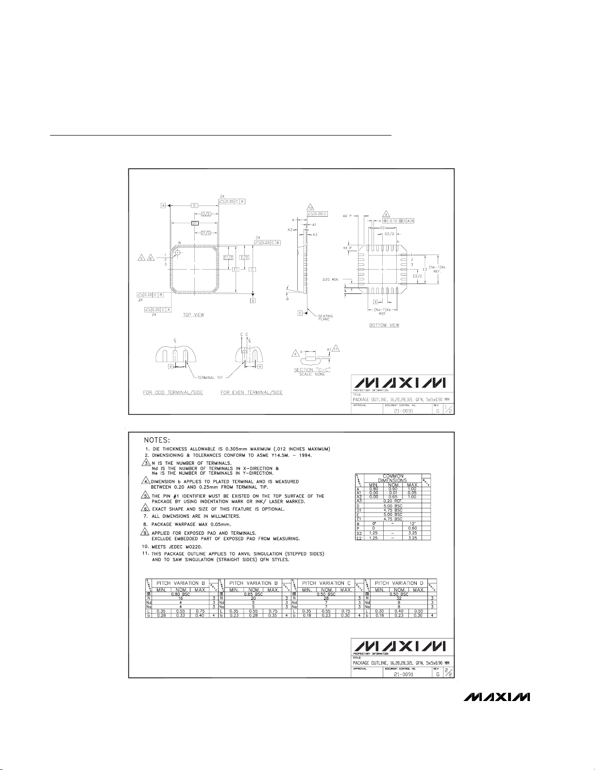
Package Information
(The package drawing(s) in this data sheet may not reflect the most current specifications. For the latest package outline information,
go to www.maxim-ic.com/packages.)
Page 11

MAX9424–MAX9427
Lowest Jitter Quad PECL-to-ECL
Differential Translators
Maxim cannot assume responsibility for use of any circuitry other than circuitry entirely embodied in a Maxim product. No circuit patent licenses are
implied. Maxim reserves the right to change the circuitry and specifications without notice at any time.
Maxim Integrated Products, 120 San Gabriel Drive, Sunnyvale, CA 94086 408-737-7600 ____________________ 11
© 2002 Maxim Integrated Products Printed USA is a registered trademark of Maxim Integrated Products.
Package Information (continued)
(The package drawing(s) in this data sheet may not reflect the most current specifications. For the latest package outline information,
go to www.maxim-ic.com/packages.)
32L TQFP, 5x5x01.0.EPS
 Loading...