

Page 1
General Description
The MAX9401/MAX9404 are extremely fast and lowskew quad ECL/PECL differential buffers/receivers for
data and clock signals. The four channels can be operated synchronously with an external clock, or in asynchronous mode, determined by the state of the SEL
input. An enable input provides the ability to force all
the outputs to a differential low state.
The MAX9401 has high-impedance (open) input and
the MAX9404 has an integrated 100Ω differential input
termination, which reduces external component count.
Both devices have double amplitude swing open emitter outputs suitable for driving long cables. The
MAX9401/MAX9404 operate over a VCC- VEE= +3.0V
to +5.5V supply range, and are specified for operation
from -40°C to +85°C. These devices are offered in
space-saving 32-pin 5mm x 5mm QFN exposed-paddle
(EP) and TQFP packages.
Applications
Data and Clock Driver and Buffer
Central Office Backplane Clock Distribution
DSLAM Backplane
Base Station
ATE
Features
♦ Differential Double-Swing ECL/PECL Outputs
♦ Input Compatible with LVECL/LVPECL
♦ Guaranteed 900mV Differential Output at 3.0GHz
Clock Rate
♦ 365ps Propagation Delay in Asynchronous Mode
♦ 10ps Channel-to-Channel Skew in Synchronous
Mode
♦ Integrated 100Ω Input Terminations (MAX9404)
♦ Compatible +3.3V/+5.0V Nominal Supplies
♦ Selectable Synchronous/Asynchronous
Operation
MAX9401/MAX9404
Quad ECL/PECL Differential
Buffers/Receivers
________________________________________________________________ Maxim Integrated Products 1
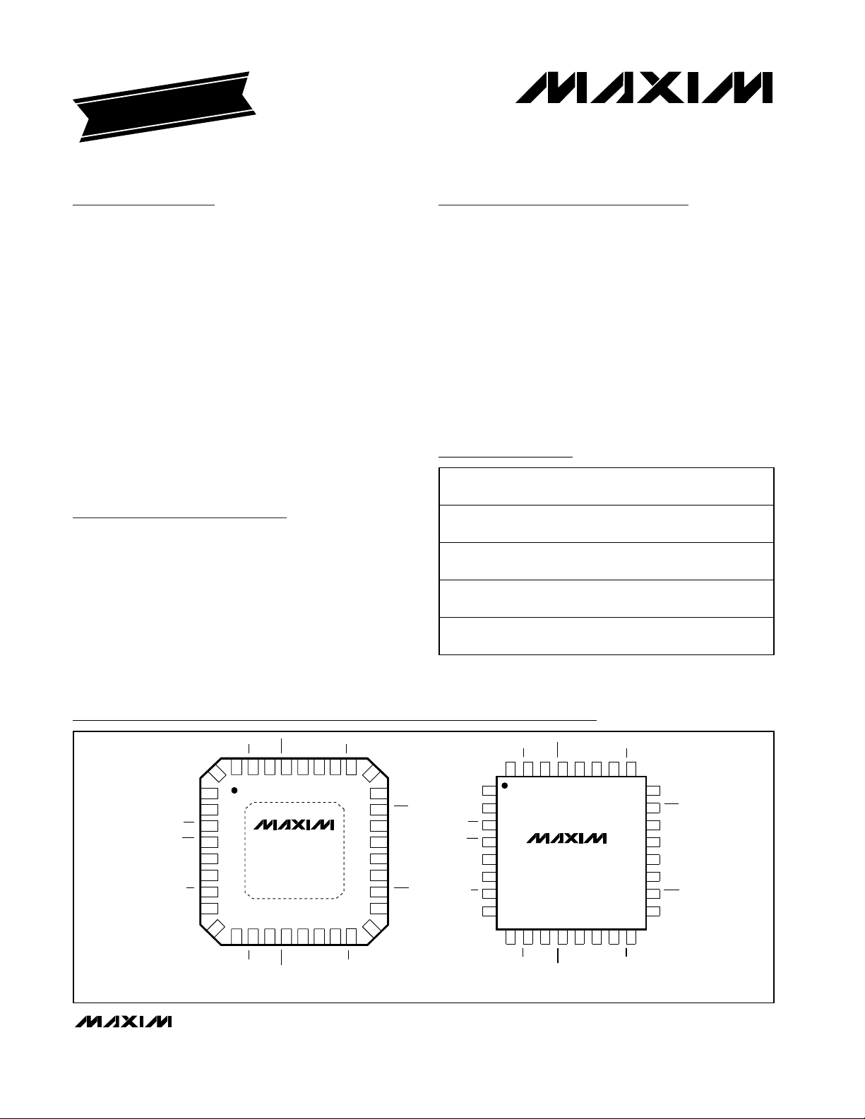
Pin Configurations
19-2245; Rev 0; 10/01
For pricing, delivery, and ordering information, please contact Maxim/Dallas Direct! at
1-888-629-4642, or visit Maxim’s website at www.maxim-ic.com.
EVALUATION KIT
AVAILABLE
*Future product—contact factory for availability.
**EP = Exposed paddle
Ordering Information
PART
TEMP.
PINPACKAGE
INPUT
IMPEDANCE
MAX9401EGJ*
-40°C to
32 QFN-EP**
Open
MAX9401EHJ
-40°C to
32 TQFP
Open
MAX9404EGJ*
-40°C to
32 QFN-EP**
100Ω
MAX9404EHJ
-40°C to
32 TQFP
100Ω
Functional Diagram appears at end of data sheet.
RANGE
+85°C
+85°C
+85°C
+85°C
(5mm x 5mm)
(5mm x 5mm)
(5mm x 5mm)
(5mm x 5mm)
TOP VIEW
**
1V
CC
SEL
2
SEL
3
CLK
4
CLK
5
EN
6
EN
7
V
8
CC
*
*EXPOSED PAD AND CORNER PINS ARE CONNECTED TO V
CC
OUT0
OUT0
OUT3
OUT3
VEEIN1
EE
V
IN0
IN0
V
32313029282726
MAX9401/
MAX9404
*
9
1011121314
CC
IN3
IN3
V
QFN-EP*
EE
25 IN1
24 V
CC
OUT1
23
OUT1
22
V
21
EE
V
20
EE
OUT2
19
OUT2
18
17
V
CC
*
15
16
IN2
IN2
VEEIN1
27
14
EE
V
IN1
26
25
24 V
CC
OUT1
23
OUT1
22
V
21
EE
V
20
EE
OUT2
19
OUT2
18
V
17
CC
15
1611 12
IN2
IN2
SEL
SEL
CLK
CLK
1V
CC
2
3
4
5
6
EN
7
EN
8V
CC
IN0
VCCOUT0
IN0
32 28
9
IN3
293031
MAX9401
MAX9404
10
CC
IN3
V
OUT3
TQFP
OUT0
13
OUT3
Page 2
MAX9401/MAX9404
Quad ECL/PECL Differential
Buffers/Receivers
2 _______________________________________________________________________________________
ABSOLUTE MAXIMUM RATINGS
Stresses beyond those listed under “Absolute Maximum Ratings” may cause permanent damage to the device. These are stress ratings only, and functional
operation of the device at these or any other conditions beyond those indicated in the operational sections of the specifications is not implied. Exposure to
absolute maximum rating conditions for extended periods may affect device reliability.
VCCto VEE.............................................................-0.3V to +6.0V
All Other Pins to V
EE
...................................-0.3V to (VCC+ 0.3V)
Differential Input Voltage….................................................±3.0V
Continuous Output Current .................................................70mA
Surge Output Current….. ..................................................100mA
Continuous Power Dissipation (T
A
= +70°C)
32-Pin 5mm x 5mm TQFP (derate 9.5mW/°C
above +70°C)..............................................................761mW
32-Pin 5mm x 5mm QFN-EP (derate 21.3mW/°C
above +70°C)..................................................................1.7W
Junction-to-Ambient Thermal Resistance in Still Air
32-Pin TQFP............................................................+105°C/W
32-Pin QFN-EP…. .....................................................+47°C/W
Junction-to-Ambient Thermal Resistance with
500LFPM Airflow
32-Pin TQFP..............................................................+73°C/W
Junction-to-Case Thermal Resistance
32-Pin TQFP..............................................................+25°C/W
32-Pin QFN-EP… ........................................................+2°C/W
Operating Temperature Range ...........................-40°C to +85°C
Junction Temperature......................................................+150°C
Storage Temperature Range .............................-65°C to +150°C
ESD Protection
Human Body Model (Inputs and Outputs).................>1.25kV
Soldering Temperature (10s) ...........................................+300°C
DC ELECTRICAL CHARACTERISTICS
(VCC- VEE= +3.0V to +5.5V, outputs terminated with 50Ω ±1% to VCC- 3.3V, inputs are driven, unless otherwise noted. Typical values are at V
CC
- VEE= +3.3V, V
IHD
= VCC- 0.9V, V
ILD
= VCC- 1.7V, TA= +25°C, unless otherwise noted.) (Notes 1, 2, 3)
INPUTS (IN_, IN_, CLK, CLK, EN, EN, SEL, SEL)
Differential Input High Voltage V
Differential Input Low Voltage V
Differential Input Voltage V
Input Current IIH, I
IN to IN Differential Input
Resistance
OUTPUTS (OUT_, OUT_)
Differential Output Voltage V
Output Common-Mode Voltage V
POWER SUPPLY
Supply Current I
PARAMETER SYMBOL CONDITIONS MIN TYP MAX UNITS
IHD
ILD
R
OH
OCM
EE
V
+
EE
Figure 3
Figure 3 V
ID
IN
Figure 3 0.2 3.0 V
MAX9401
IL
MAX9404
EN, EN, SEL, SEL, IN_, IN_,
CLK, or CLK = V
IHD
or V
ILD
EN, EN , SEL, SEL, CLK, or
CLK = V
IHD
or V
ILD
MAX9404 86 114 Ω
2.0
EE
-10 25
-10 25
V
CC
V
-
CC
0.2
- V OLFigure 3 1.2 1.4 V
Figure 3
-
V
CC
1.8
V
-
CC
1.4
(Note 4) 84 118 mA
V
V
µA
V
Page 3
MAX9401/MAX9404
Quad ECL/PECL Differential
Buffers/Receivers
_______________________________________________________________________________________ 3
Note 1: Measurements are made with the device in thermal equilibrium.
Note 2: Current into a pin is defined as positive. Current out of a pin is defined as negative. All voltages are referenced to V
EE
except VIDand VOD.
Note 3: DC parameters are production tested at T
A
= +25°C. DC limits are guaranteed by design and characterization over the full
operating range.
Note 4: Outputs are open. Inputs driven high or low.
Note 5: Guaranteed by design and characterization. Limits are set to ±6 sigma.
Note 6: Measured between outputs of the same part at the signal crossing points for a same-edge transition.
Note 7: Device jitter added to the input signal.
AC ELECTRICAL CHARACTERISTICS
(VCC- VEE= +3.0V to +5.5V, outputs terminated with 50Ω ±1% to VCC- 3.3V, outputs are enabled, input transition time = 125ps
(20% to 80%), f
CLK
= 3.0GHz, fIN= 1.5GHz, V
IHD
= VEE+2.0V to VCC, V
ILD
= VEEto VCC- 0.2V, V
IHD
- V
ILD
= 0.2 to 3.0V, unless oth-
erwise noted. Typical values are at V
CC
- VEE= +3.3V, V
IHD
= VCC- 0.9V, V
ILD
= VCC- 1.7V, TA= +25°C, unless otherwise noted.)
(Notes 1, 5)
)
(
)
p-p
PARAMETER SYMBOL CONDITIONS MIN TYP MAX UNITS
IN to OUT Differential
Propagation Delay
CLK to OUT Differential
Propagation Delay
IN to OUT Channel-to-Channel
Skew
CLK to OUT Channel-toChannel Skew
Maximum Clock Frequency f
Maximum Data Frequency f
Added Random Jitter (Note 7) t
Added Deterministic Jitter
(Note 7)
IN to CLK Setup Time t
CLK to IN Hold Time t
Output Rise Time t
Output Fall Time t
Propagation Delay Temperature
Coefficient
, t
t
P LH 1
P H L 1
t
, t
P LH 2
P H L 2
t
SKD1
t
SKD2
CLK(MAX
IN(MAX)
RJ
SEL = high, Figure 4 300 365 550 ps
SEL = low, Figure 5 580 620 758 ps
SEL = high (Note 6) 15 55 ps
SEL = low (Note 6) 10 40 ps
VOH - VOL ≥ 900mV, SEL = low 3.0 GHz
SEL = high, VOH - VOL ≥ 900mV 1.5 GHz
SEL = low, fIN = 1.5GHz, f
clock
= 3.0GHz,
CLK
1.4 2.5
SEL = high, fIN = 1.5GHz 0.9 2.7
SEL = low, f
23
-1 PRBS pattern
t
DJ
2
SEL = high, IN_ = 1.5Gbps, 223-1 PRBS
pattern
S
H
R
F
/∆T 1 ps/°C
∆t
PD
Figure 5 80 ps
Figure 5 80 ps
Figure 4 116 145 ps
Figure 4 115 145 ps
= 3.0GHz, IN_ = 1.5Gbps,
CLK
20 30
36 55
ps
RMS
ps
Page 4
MAX9401/MAX9404
Quad ECL/PECL Differential
Buffers/Receivers
4 _______________________________________________________________________________________
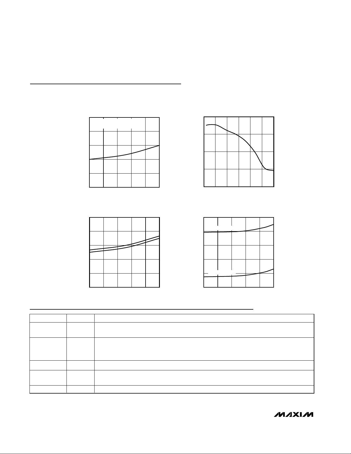
Typical Operating Characteristics
(Outputs terminated with 50Ω to VCC- 3.3V, VCC- VEE= +3.3V, V
IHD
= VCC- 0.9V, V
ILD
= VCC- 1.7V, output is enabled, SEL = high,
SEL = low, input transition time = 125ps (20% to 80%), f
CLK
= 3.0GHz, fIN= 1.5GHz, TA= +25°C, unless otherwise noted.)
70
76
88
82
94
100
-40 10-15 35 60 85
SUPPLY CURRENT vs. TEMPERATURE
MAX9401/04 toc01
TEMPERATURE (°C)
SUPPLY CURRENT (mA)
OUTPUTS ARE OPEN; INPUTS
ARE HIGH OR LOW
1.6
1.2
0.8
0.4
0
0 1.50.5 1.0 2.0 2.5 3.0
DIFFERENTIAL OUTPUT VOLTAGE
(V
OH
- VOL) vs. IN_ FREQUENCY
MAX9401/04 toc02
IN_ FREQUENCY (GHz)
DIFFERENTIAL OUTPUT VOLTAGE (mV)
100
106
118
112
124
130
-40 10-15 35 60 85
TRANSITION TIME vs. TEMPERATURE
MAX9401/04 toc03
TEMPERATURE (°C)
TRANSITION TIME (ps)
t
R
t
F
300
380
540
460
620
700
-40 10-15 35 60 85
PROPAGATION DELAY
vs. TEMPERATURE
MAX9401/04 toc04
TEMPERATURE (°C)
PROPAGATION DEALY (ps)
IN-TO-OUT DELAY
CLK-TO-OUT DELAY
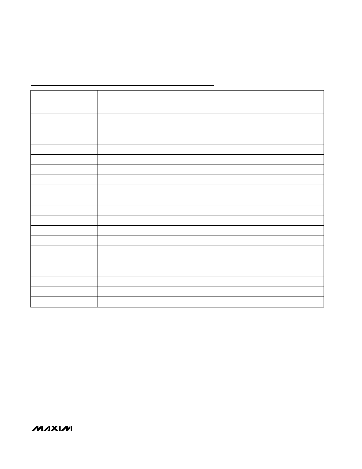
Pin Description
PIN NAME FUNCTION
1, 8, 11, 17,
24, 30
2 SEL
3 SEL Inverting Differential Select Input
4 CLK
5 CLK Noninverting Differential Clock Input
V
CC
Positive Supply Voltage. Bypass VCC to VEE with 0.1µF and 0.01µF ceramic capacitors. Place the
capacitors as close to the device as possible with the smaller value capacitor closest to the device.
Noninverting Differential Select Input. Setting SEL = high and SEL = low (differential high) enables
all four channels to operate asynchronously. Setting SEL = low and SEL = high (differential low)
enables all four channels to operate in synchronized mode.
Inverting Differential Clock Input. A rising edge on CLK (and falling on CLK) transfers data from the
inputs to the outputs when SEL = low.
Page 5
Detailed Description
The MAX9401/MAX9404 are extremely fast, low-skew
quad ECL/PECL buffers/receivers designed for highspeed data and clock driver applications. These
devices feature ultra-low propagation delay of 365ps
and channel-to-channel skew of 15ps in asynchronous
mode with 84mA supply current, making them ideal for
driving long cables and double termination applications
(Functional Diagram).
The four channels can be operated synchronously with
an external clock, or in asynchronous mode, determined by the state of the SEL input. An enable input
provides the ability to force all the outputs to a differential low state.
Data Input Termination
Figure 1 shows the input and output configuration of
the MAX9401/MAX9404. The MAX9401 has highimpedance inputs and requires external termination.
The MAX9404 has integrated 100Ω differential input
termination resistors across each of the four inputs (IN_
to IN_), reducing external component count.
Outputs
The MAX9401/MAX9404 have double-swing open-emitter outputs as shown in Figure 1. The double-amplitude
swing outputs can drive double-terminated links or long
MAX9401/MAX9404
Quad ECL/PECL Differential
Buffers/Receivers
_______________________________________________________________________________________ 5
*QFN-EP package only.
Pin Description (continued)
PIN NAME FUNCTION
6EN
7 EN Inverting Differential Output Enable Input
9 IN3 Noninverting Differential Input 3
10 IN3 Inverting Differential Input 3
12 OUT3 Inverting Differential Output 3
13 OUT3 Noninverting Differential Output 3
14, 20, 21, 27 V
15 IN2 Noninverting Differential Input 2
16 IN2 Inverting Differential Input 2
18 OUT2 Inverting Differential Output 2
19 OUT2 Noninverting Differential Output 2
22 OUT1 Noninverting Differential Output 1
23 OUT1 Inverting Differential Output 1
25 IN1 Inverting Differential Input 1
26 IN1 Noninverting Differential Input 1
EE
Noninverting Differential Output Enable Input. Setting EN = high and EN = low (differential high)
enables the outputs. Setting EN = low and EN = high (differential low) sets the outputs to logic low.
Negative Supply Voltage
28 OUT0 Noninverting Differential Output 0
29 OUT0 Inverting Differential Output 0
31 IN0 Inverting Differential Input 0
32 IN0 Noninverting Differential Input 0
— EP* Exposed Paddle. EP is electrically connected to VEE. Solder EP to PC board.
Page 6

MAX9401/MAX9404
cables. External termination is required. See the Output
Termination section.
Enable
Setting EN = high and EN = low enables the outputs.
Setting EN = low and EN = high forces the outputs to a
differential low when disabled. All changes on CLK,
SEL, and IN_ are ignored.
Asynchronous Operation
Setting SEL = high and SEL = low enables four channels to operate independently as a buffer/receiver
(CLK is ignored). In asynchronous mode, the CLK sig-
nal should be set to either logic low or high state to minimize noise coupling.
Synchronous Operation
Setting SEL = low and SEL = high enables all four
channels to operate in synchronous mode. In this
mode, buffered inputs are clocked into flip-flops simultaneously on every rising edge of the differential clock
input (CLK and CLK).
Differential Signal Input Limit
The maximum differential input signal magnitude is 3.0V.
Supply Voltages
For interfacing to differential PECL signals, the V
CC
range is from +3.0V to +5.5V (with VEEgrounded). For
interfacing to differential ECL, the VEErange is -3.0V to
-5.5V (with VCCgrounded). Output levels are referenced to VCCand are considered PECL or ECL,
depending on the level of the V
CC
supply.
Applications Information
Input Bias
Unused inputs should be biased to avoid noise coupling that might cause toggling at the unused outputs.
See Figure 2 for the biasing network.
Output Termination
Terminate the outputs through 50Ω to VCC- 3.3V or use
an equivalent Thevenin termination. Use identical terminations on each OUT for the lowest skew. When a single-ended signal is taken from a differential output,
terminate both outputs. For example, if OUT_ is used as
a single-ended output, terminate both OUT_ and OUT_.
Quad ECL/PECL Differential
Buffers/Receivers
6 _______________________________________________________________________________________
Figure 1. MAX9401/MAX9404 Input and Output Configurations
Figure 2. Input Bias Circuits for Unused Pins for MAX9401/MAX9404
IN_
IN_
MAX9401
MAX9401
MAX9404
IN_
IN_
MAX9404
V
CC
OUT_
OUT_
100Ω
V
CC
IN_
100Ω
IN_
1kΩ
MAX9401 MAX9404
V
EE
IN_
100Ω
IN_
1kΩ
V
CC
V
EE
Page 7
Ensure that the output currents do not exceed the current limits as specified in the Absolute Maximum
Ratings. Under all operating conditions, the device’s
total thermal limits should be observed.
Power-Supply Bypassing
Adequate power-supply bypassing is necessary to
maximize the performance and noise immunity. Bypass
VCCto VEEwith high-frequency surface-mount ceramic
0.1µF and 0.01µF capacitors as close to the device as
possible, with the 0.01µF capacitor closest to the
device pins. Use multiple bypass vias for connection to
minimize inductance.
Circuit Board Traces
Input and output trace characteristics affect the performance of the MAX9401/MAX9404. Connect each of the
inputs and outputs to a 50Ω characteristic impedance
trace. Avoid discontinuities in differential impedance
and maximize common-mode noise immunity by main-
MAX9401/MAX9404
Quad ECL/PECL Differential
Buffers/Receivers
_______________________________________________________________________________________ 7
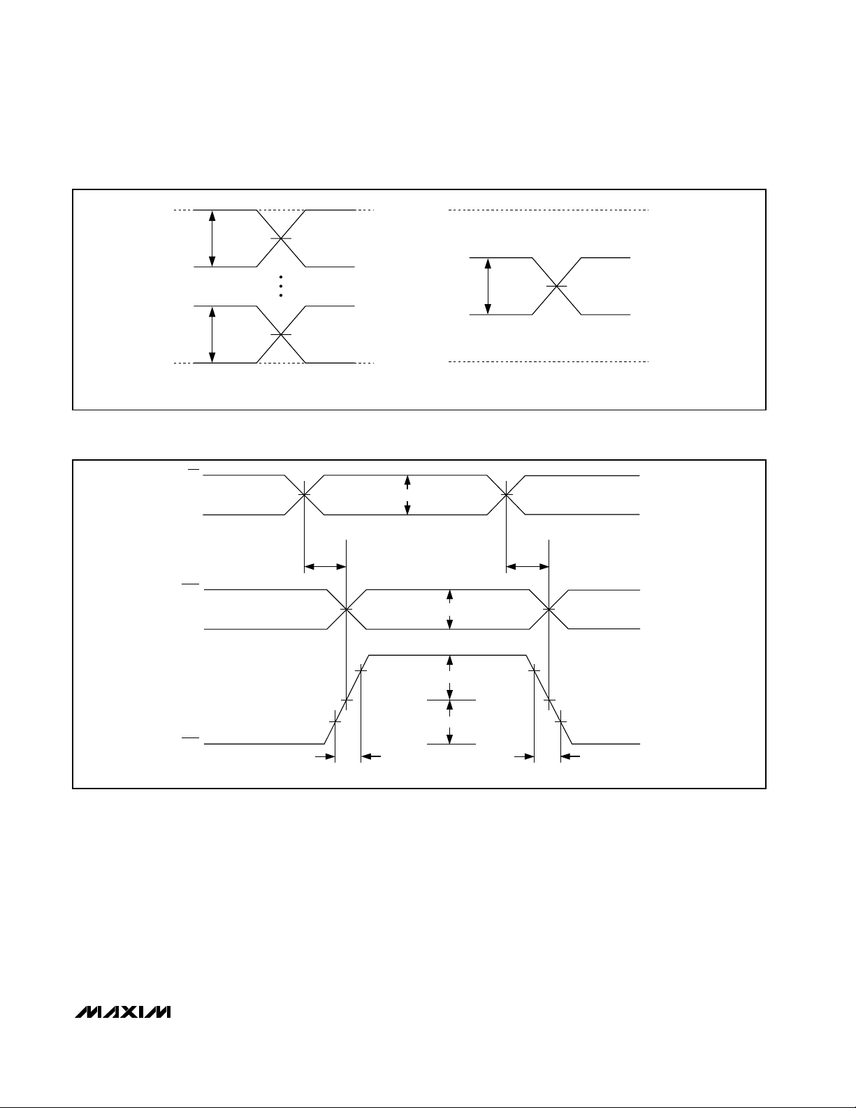
Figure 3. Input and Output Voltage Definitions
Figure 4. IN to OUT Propagation Delay Timing Diagram
V
CC
V
ID
V
ID
V
EE
INPUT VOLTAGE DEFINITION OUTPUT VOLTAGE DEFINITION
V
V
IN_
IN_
OUT_
OUT_
(MAX) V
V
IHD
= 0
ID
V
(MAX)
ILD
V
- V
OH
OL
V
(MIN)
IHD
= 0
ID
V
(MIN)
ILD
V
- V
IHD
ILD
t
PLH1
VOH - V
OL
t
PHL1
V
OCM
CC
V
OH
V
OL
V
EE
80%
20% 20%
t
R
OUT_ - OUT_
DIFFERENTIAL OUTPUT
WAVEFORM
VOH - V
VOH - V
OL
OL
80%
t
F
(SEL = HIGH, EN = HIGH)
Page 8
MAX9401/MAX9404
taining the distance between differential traces and
avoid sharp corners. Minimize the number of vias to
prevent impedance discontinuities. Reduce reflections
by maintaining the 50Ω characteristic impedance
through connectors and across cables. Minimize skew
by matching the electrical length of the traces.
Chip Information
TRANSISTOR COUNT: 748
PROCESS: Bipolar
Quad ECL/PECL Differential
Buffers/Receivers
8 _______________________________________________________________________________________
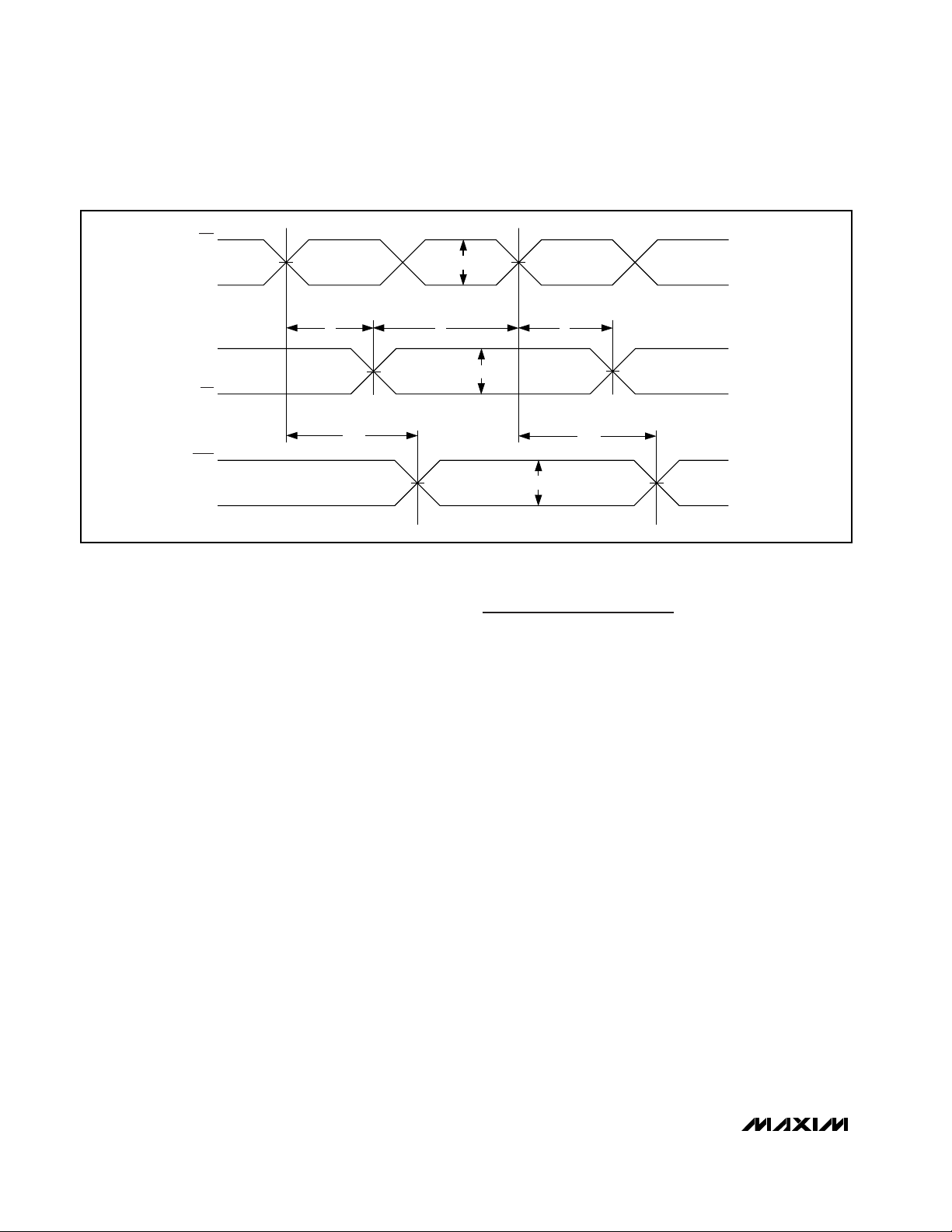
Figure 5. CLK to OUT Propagation Delay Timing Diagram
CLK
V
- V
IHD
ILD
CLK
t
H
IN_
IN_
t
PLH2
OUT_
OUT_
t
S
V
- V
IHD
ILD
VOH - V
OL
t
H
t
PHL2
(SEL = LOW, EN = HIGH)
Page 9

MAX9401/MAX9404
Quad ECL/PECL Differential
Buffers/Receivers
_______________________________________________________________________________________ 9
Functional Diagram
IN0
IN0
IN1
IN1
IN2
IN2
DQ
Q
D
CLK
CLK
D
Q
D
Q
CLK
CLK
D
Q
D
Q
CLK
CLK
1
0
1
0
1
0
OUT0
OUT0
OUT1
OUT1
OUT2
OUT2
IN3
IN3
CLK
CLK
SEL
SEL
1
D
Q
D
Q
CLK
CLK
EN
EN
0
OUT3
OUT3
Page 10
MAX9401/MAX9404
Quad ECL/PECL Differential
Buffers/Receivers
10 ______________________________________________________________________________________
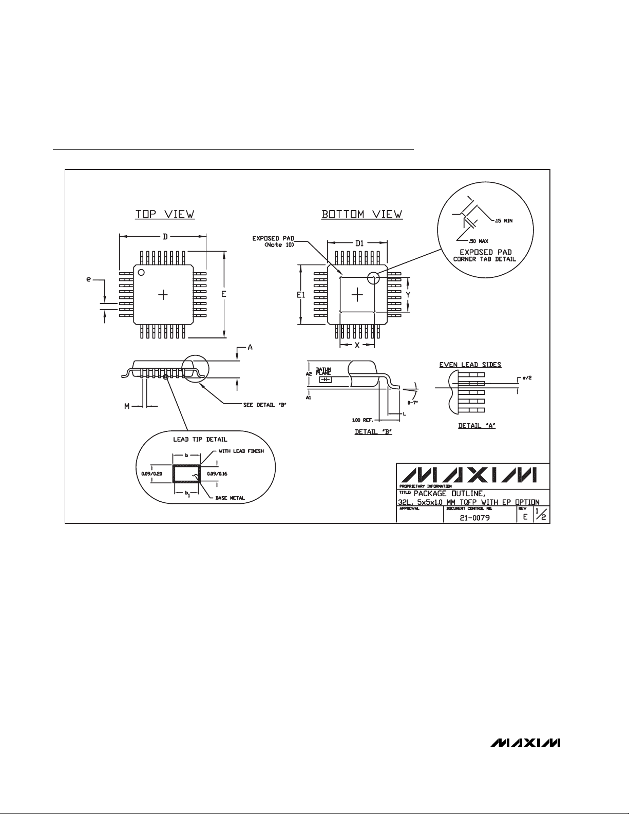
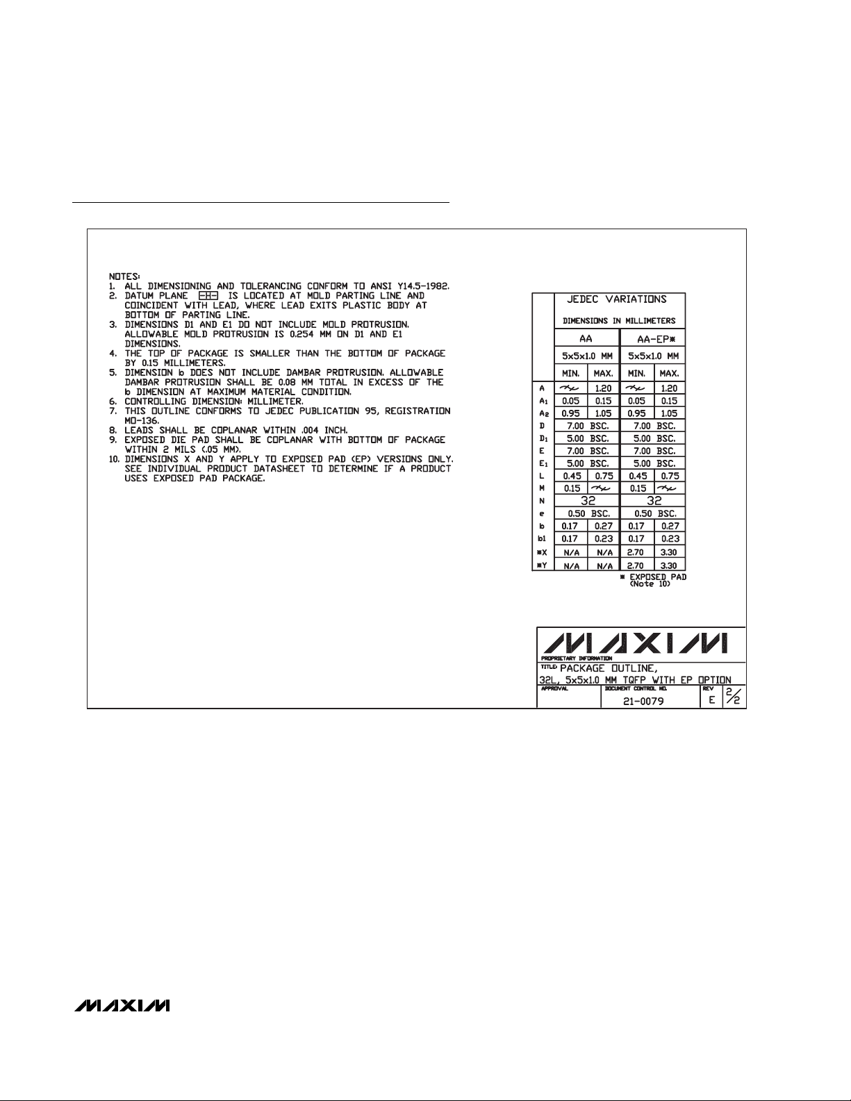
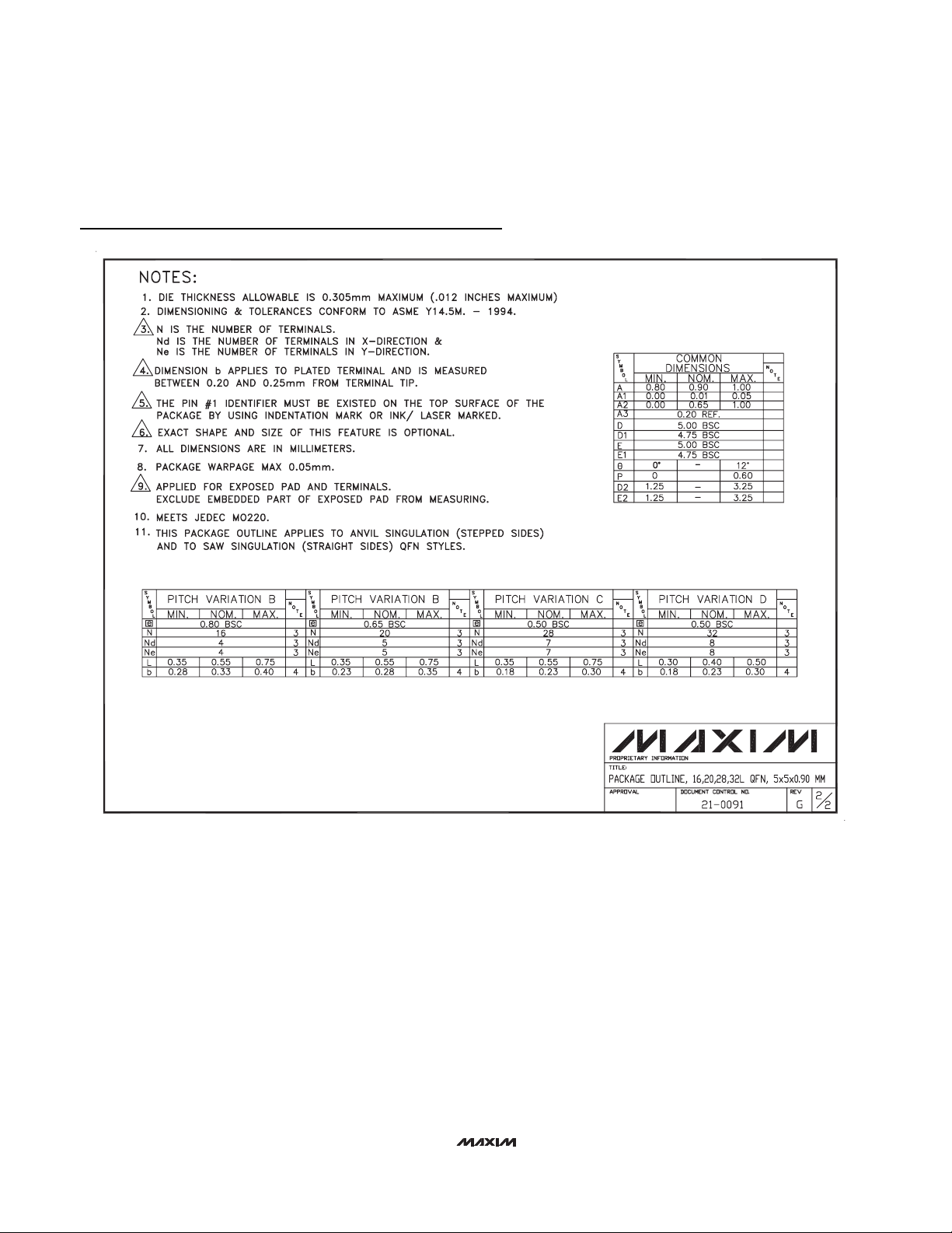
Package Information
32L,TQFP.EPS
Page 11
MAX9401/MAX9404
Quad ECL/PECL Differential
Buffers/Receivers
______________________________________________________________________________________ 11
Package Information (continued)
Page 12

MAX9401/MAX9404
Quad ECL/PECL Differential
Buffers/Receivers
12 ______________________________________________________________________________________
Package Information (continued)
Page 13
MAX9401/MAX9404
Quad ECL/PECL Differential
Buffers/Receivers
Maxim cannot assume responsibility for use of any circuitry other than circuitry entirely embodied in a Maxim product. No circuit patent licenses are
implied. Maxim reserves the right to change the circuitry and specifications without notice at any time.
Maxim Integrated Products, 120 San Gabriel Drive, Sunnyvale, CA 94086 408-737-7600 ____________________ 13
© 2001 Maxim Integrated Products Printed USA is a registered trademark of Maxim Integrated Products.
Package Information (continued)
 Loading...