

Page 1
General Description
The MAX9394/MAX9395 consist of a 2:1 multiplexer
and a 1:2 demultiplexer with loopback. The multiplexer
section (channel B) accepts two low-voltage differential
signaling (LVDS) inputs and generates a single LVDS
output. The demultiplexer section (channel A) accepts
a single LVDS input and generates two parallel LVDS
outputs. The MAX9394/MAX9395 feature a loopback
mode that connects the input of channel A to the output
of channel B and connects the selected input of channel B to the outputs of channel A.
Three LVCMOS/LVTTL logic inputs control the internal
connections between inputs and outputs, one for the
multiplexer portion of channel B (BSEL), and the other
two for loopback control of channels A and B (LB_SELA
and LB_SELB). Independent enable inputs for each differential output pair provide additional flexibility.
Fail-safe circuitry forces the outputs to a differential low
condition for undriven inputs or when the commonmode voltage exceeds the specified range. The
MAX9394 provides high-level input fail-safe detection
for HSTL, LVDS, and other GND-referenced differential
inputs. The MAX9395 provides low-level fail-safe detection for CML, LVPECL, and other VCC-referenced differential inputs.
Ultra low 91ps
P-P
(max) pseudorandom bit sequence
(PRBS) jitter ensures reliable communications in highspeed links that are highly sensitive to timing error,
especially those incorporating clock-and-data recovery,
or serializers and deserializers. The high-speed switching performance guarantees 1.5GHz operation and less
than 87ps (max) skew between channels.
LVDS inputs and outputs are compatible with the
TIA/EIA-644 LVDS standard. The LVDS outputs drive
100Ω loads. The MAX9394/MAX9395 are offered in a
32-pin TQFP package and operate over the extended
temperature range (-40°C to +85°C).
Applications
High-Speed Telecom/Datacom Equipment
Central Office Backplane Clock Distribution
DSLAM
Protection Switching
Fault-Tolerant Systems
Features
♦ Guaranteed 1.5GHz Operation with 250mV
Differential Output Swing
♦ Simultaneous Loopback Control
♦ 2ps
(RMS)
(max) Random Jitter
♦ AC Specifications Guaranteed for 150mV
Differential Input
♦ Signal Inputs Accept Any Differential Signaling
Standard
♦ LVDS Outputs for Clock or High-Speed Data
♦ High-Level Input Fail-Safe Detection (MAX9394)
♦ Low-Level Input Fail-Safe Detection (MAX9395)
♦ 3.0V to 3.6V Supply Voltage Range
♦ LVCMOS/LVTTL Logic Inputs
MAX9394/MAX9395
2:1 Multiplexers and 1:2 Demultiplexers with
Loopback
________________________________________________________________ Maxim Integrated Products 1
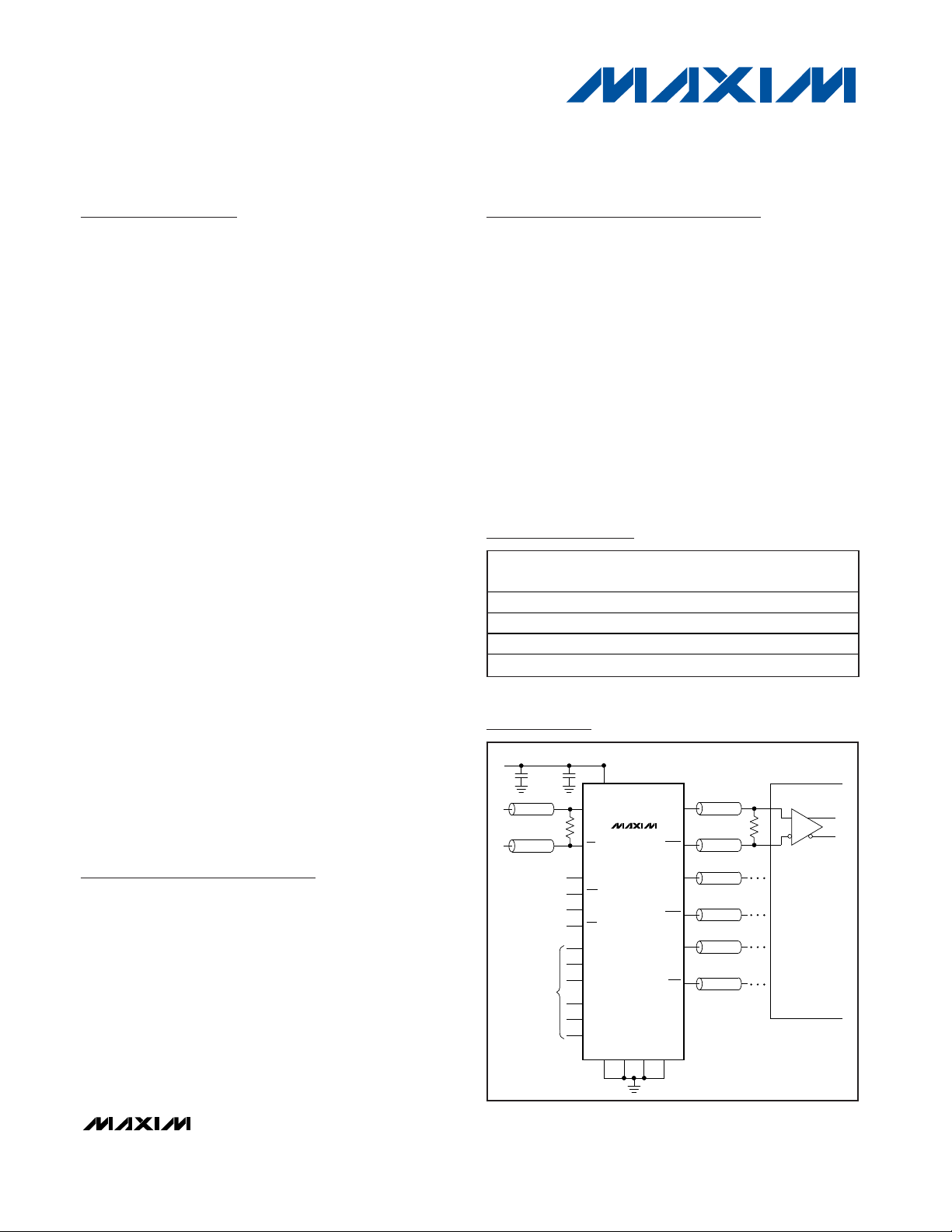
Ordering Information
0.1μF 0.01μF
3.0V TO
3.6V
OUTA0
OUTA0
LVDS
RECEIVER
INA
INA
ENA0
ENA1
ENB
GNDGND GNDGND
OUTA1
OUTA1
OUTB
OUTB
LVCMOS/LVTTL
LOGIC INPUTS
LB_SELA
LB_SELB
BSEL
INB0
INB0
100Ω
Z0 = 50Ω
Z0 = 50Ω
MAX9394
MAX9395
V
CC
INB1
INB1
Z0 = 50Ω
Z0 = 50Ω
100Ω
Z0 = 50Ω
Z0 = 50Ω
Z0 = 50Ω
Z0 = 50Ω
Typical Operating Circuit
19-2878; Rev 1; 5/07
For pricing, delivery, and ordering information, please contact Maxim/Dallas Direct! at
1-888-629-4642, or visit Maxim’s website at www.maxim-ic.com.
PART TEMP RANGE
PINPACKAGE
PKG
CODE
MAX9394EHJ
32 TQFP
H32-1
MAX9394EHJ+
32 TQFP
H32-1
MAX9395EHJ
32 TQFP
H32-1
MAX9395EHJ+
32 TQFP
H32-1
Pin Configurations and Functional Diagram appear at end
of data sheet.
+Denotes a lead-free package.
-40°C to +85°C
-40°C to +85°C
-40°C to +85°C
-40°C to +85°C
Page 2
MAX9394/MAX9395
2:1 Multiplexers and 1:2 Demultiplexers with
Loopback
2 _______________________________________________________________________________________
ABSOLUTE MAXIMUM RATINGS
Stresses beyond those listed under “Absolute Maximum Ratings” may cause permanent damage to the device. These are stress ratings only, and functional
operation of the device at these or any other conditions beyond those indicated in the operational sections of the specifications is not implied. Exposure to
absolute maximum rating conditions for extended periods may affect device reliability.
VCCto GND...........................................................-0.3V to +4.1V
IN_ _,
IN_ _, OUT_ _, OUT_ _, EN_ _, _SEL, LB_SEL_
to GND........................................................-0.3V to (V
CC
+ 0.3V)
IN_ _ to IN_ _..........................................................................±3V
Short-Circuit Duration (OUT_ _, OUT_ _) ...................Continuous
Continuous Power Dissipation (T
A
= +70°C)
32-Pin TQFP (derate 13.1mW/°C above +70°C)........1047mW
Junction-to-Ambient Thermal Resistance in Still Air
32-Pin TQFP............................................................+76.4°C/W
Operating Temperature Range ...........................-40°C to +85°C
Junction Temperature......................................................+150°C
Storage Temperature Range .............................-65°C to +150°C
ESD Protection (Human Body Model)
(IN_ _, IN_ _, OUT_ _, OUT_ _, EN_ _, SEL_, LB_SEL_) ..±2kV
Soldering Temperature (10s) ...........................................+300°C
DC ELECTRICAL CHARACTERISTICS
(VCC= 3.0V to 3.6V, RL= 100Ω ±1%, EN_ _ = VCC, VCM= +0.05V to (VCC- 0.6V) (MAX9394), VCM= +0.06V to (VCC- 0.05V)
(MAX9395), T
A
= -40°C to +85°C, unless otherwise noted. Typical values are at VCC= 3.3V, |VID| = 0.2V, VCM= 1.2V, TA= +25°C.)
(Notes 1, 2, and 3)
PARAMETER
CONDITIONS
UNITS
LVCMOS/LVTTL INPUTS (EN_ _, BSEL, LB_SEL_)
Input High Voltage V
IH
2.0
V
Input Low Voltage V
IL
0 0.8 V
Input High Current I
IH
VIN = 2.0V to V
CC
020µA
Input Low Current I
IL
VIN = 0V to 0.8V 0 10 µA
DIFFERENTIAL INPUTS (IN_ _, IN_ _)
Differential Input Voltage V
ID
V
ILD
>
0V and V
IHD
<
VCC, Figure 1 0.1 3.0 V
MAX9394
VCC -
0.6
Input Common-Mode Range V
CM
MAX9395 0.6
V
CC
-
V
MAX9394 |VID|
<
3.0V -75 10
Input Current
I
IN_ _
,
I
IN_ _ MAX9395 |V
ID
|
<
3.0V -10 100
µA
LVDS OUTPUTS (OUT_ _, OUT_ _)
Differential Output Voltage V
OD
RL = 100Ω, Figure 2 250
450 mV
Change in Magnitude of V
OD
Between Complementary Output
States
ΔV
OD
Figure 2 1.0 50 mV
Offset Common-Mode Voltage V
OS
Figure 2
V
Change in Magnitude of V
OS
Between Complementary Output
States
ΔV
OS
Figure 2 1.0 50 mV
SYM B O L
MIN TYP MAX
0.05
1.125 1.25 1.375
350
V
CC
0.05
Page 3
MAX9394/MAX9395
2:1 Multiplexers and 1:2 Demultiplexers with
Loopback
_______________________________________________________________________________________ 3
PARAMETER
SYM B O L
CONDITIONS
MIN
TYP
MAX
UNITS
30 40
Output Short-Circuit Current
(Output(s) Shorted to GND)
|I
OS
|
V
ID
= ±100mV
(Note 4)
V
OUT_ _
=
V
OUT_ _
= 0V
17 24
mA
Output Short-Circuit Current
(Outputs Shorted Together)
|I
OSB
|
512mA
SUPPLY CURRENT
RL = 100Ω, EN_ _ = V
CC
53 65
Supply Current I
CC
RL = 100Ω, EN_ _ = VCC, switching at
670MHz (1.34Gbps)
53 65
mA
Note 1: Measurements obtained with the device in thermal equilibrium. All voltages referenced to GND except VID, VOD, and ΔVOD.
Note 2: Current into the device defined as positive. Current out of the device defined as negative.
Note 3: DC parameters production tested at T
A
= +25°C and guaranteed by design and characterization for TA= -40°C to +85°C.
Note 4: Current through either output.
Note 5: Guaranteed by design and characterization. Limits set at ±6 sigma.
Note 6: t
SKEW
is the magnitude difference of differential propagation delays for the same output over the same condtions. t
SKEW
=
|t
PHL
- t
PLH
|.
Note 7: Measured between outputs of the same device at the signal crossing points for a same-edge transition under the same con-
ditions. Does not apply to loopback mode.
Note 8: Device jitter added to the differential input signal.
DC ELECTRICAL CHARACTERISTICS (continued)
(VCC= 3.0V to 3.6V, RL= 100Ω ±1%, EN_ _ = VCC, VCM= 0.05V to (VCC- 0.6V) (MAX9394), VCM= 0.06V to (VCC- 0.05V)
(MAX9395), T
A
= -40°C to +85°C, unless otherwise noted. Typical values are at VCC= 3.3V, |VID| = 0.2V, VCM= 1.2V, TA= +25°C.)
(Notes 1, 2, and 3)
AC ELECTRICAL CHARACTERISTICS
(VCC= 3.0V to 3.6V, fIN< 1.34GHz, t
R_IN
= t
F_IN
= 125ps, RL= 100Ω ±1%, |VID| ≥ 150mV, VCM= 0.075V to (VCC- 0.6V) (MAX9394
only), V
CM
= 0.6V to (VCC- 0.075V) (MAX9395 only), EN_ _ = VCC, TA= -40°C to +85°C, unless otherwise noted. Typical values are
at V
CC
= 3.3V, |VID| = 0.2V, VCM= 1.2V, fIN= 1.34GHz, TA= +25°C.) (Note 5)
PARAMETER
SYM B O L
CONDITIONS
MIN
TYP
MAX
UNITS
SEL to Switched Output
Figure 3 1.1 ns
Disable Time to Differential
Output Low
t
PHD
Figure 4 1.7 ns
Enable Time to Differential Output
High
t
PDH
Figure 4 1.7 ns
Switching Frequency f
MAX
VOD
>
250mV 1.5 2.2 GHz
Low-to-High Propagation Delay t
PLH
Figures 1, 5
ps
High-to-Low Propagation Delay t
PHL
Figures 1, 5
ps
Pulse Skew |t
PLH
– t
PHL
|t
SKEW
Figures 1, 5 (Note 6)
86 ps
Output Channel-to-Channel Skew
t
CCS
Figure 6 (Note 7) 16 87 ps
Output Low-to-High Transition
Time (20% to 80%)
t
R
f
IN_ _
= 100MHz, Figures 1, 5
ps
Output High-to-Low Transition
Time (80% to 20%)
t
F
f
IN_ _
= 100MHz, Figures 1, 5
ps
Added Random Jitter t
RJ
f
IN_ _
= 1.34GHz, clock pattern (Note 8) 2
ps
(RMS)
Added Deterministic Jitter t
DJ
1.34Gbps, 223 - 1 PRBS (Note 8) 60 91
ps
P-P
V
VID = ±100mV, V
OUT_ _
OUT_ _
= V
or V
OUT_ _
OUT_ _
(Note 4)
= 0V
t
SWITCH
340 567 720
340 562 720
112 154 187
112 152 187
12.4
Page 4
MAX9394/MAX9395
2:1 Multiplexers and 1:2 Demultiplexers with
Loopback
4 _______________________________________________________________________________________
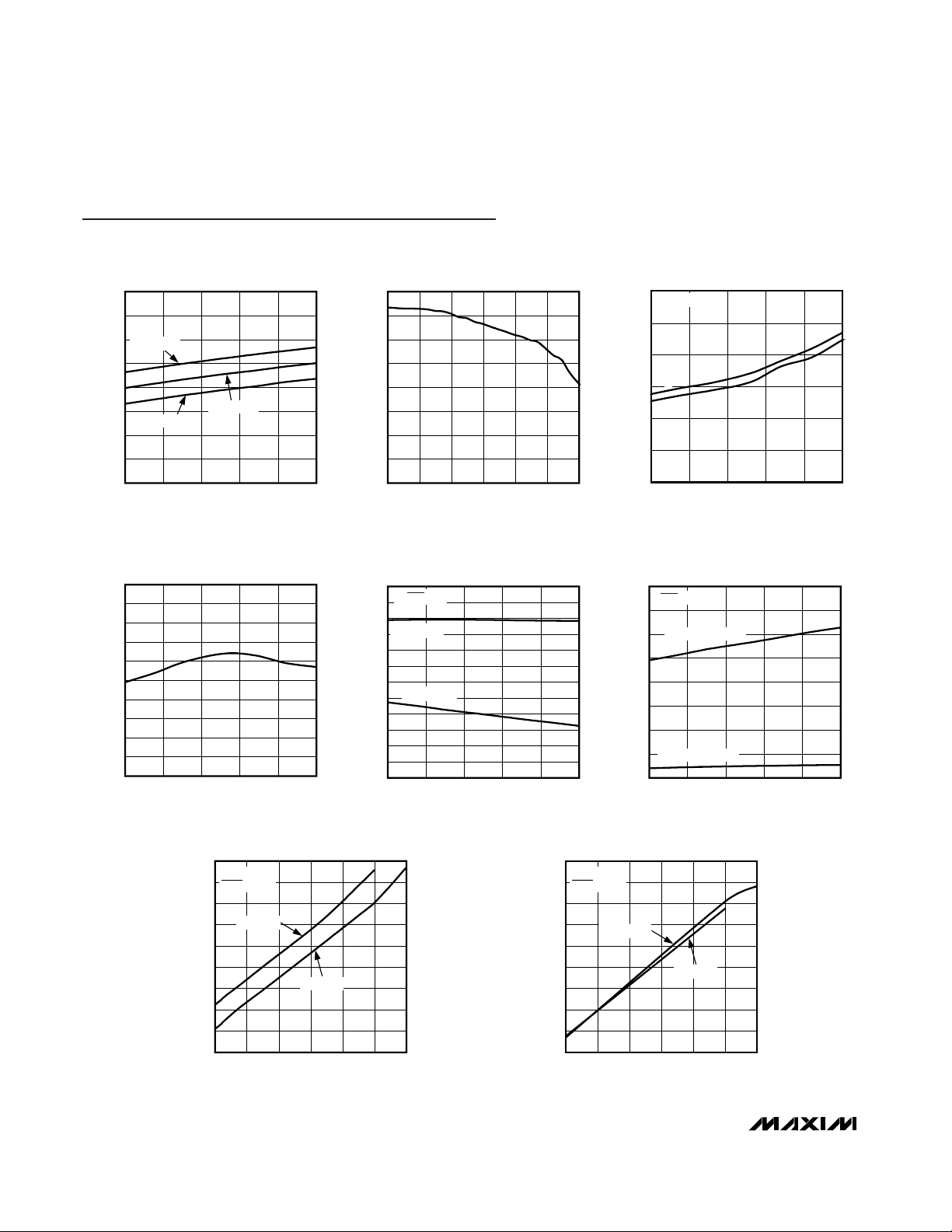
Typical Operating Characteristics
(VCC= 3.3V, |VID| = 0.2V, VCM= +1.2V, TA= +25°C, fIN= 1.34GHz, Figure 5.)
SUPPLY CURRENT vs. TEMPERATURE
MAX9394/95 toc01
TEMPERATURE (°C)
SUPPLY CURRENT (mA)
6035-15 10
35
40
45
50
55
60
65
70
30
-40 85
VCC = 3.3V
VCC = 3.6V
VCC = 3.0V
OUTPUT AMPLITUDE vs. FREQUENCY
MAX9394/95 toc02
FREQUENCY (GHz)
OUTPUT AMPLITUDE (mV)
2.00.4 1.2 1.60.8
50
100
150
200
250
300
350
400
0
0 2.4
OUTPUT RISE/FALL TIME
vs. TEMPERATURE
MAX9394/95 toc03
TEMPERATURE (°C)
RISE/FALL TIME (ps)
603510-15
130
140
150
160
170
180
120
-40 85
t
R
t
F
fIN = 100MHz
PROPAGATION DELAY
vs. TEMPERATURE
MAX9394/95 toc04
TEMPERATURE (°C)
PROPAGATION DELAY (ps)
603510-15
510
520
530
540
550
560
570
580
590
600
500
-40 85
MAX9394 DIFFERENTIAL INPUT CURRENT
vs. TEMPERATURE
MAX9394/95 toc05
TEMPERATURE (°C)
INPUT CURRENT (μA)
603510-15
-45
-40
-35
-30
-25
-20
-15
-10
-5
0
5
10
-50
-40 85
V
IN_ _
= 3.0V
V
IN_ _
= 0.1V
V
IN_ _
= 0V
MAX9395 DIFFERENTIAL INPUT CURRENT
vs. TEMPERATURE
MAX9394/95 toc06
TEMPERATURE (°C)
INPUT CURRENT (μA)
6035-15 10
10
20
30
40
50
60
70
80
0
-40 85
V
IN_ _
= V
CC
V
IN_ _
= (VCC - 0.1V)
V
IN_ _
= (VCC - 3.0V)
MAX9394
DIFFERENTIAL INPUT CURRENT vs. V
IHD
MAX9394/95 toc07
V
IHD
(V)
INPUT CURRENT (μA)
3.02.40.6 1.2 1.8
-35
-30
-25
-20
-15
-10
-5
0
5
-40
0 3.6
IN_ _ OR
IN_ _ = GND
VCC = 3V
VCC = 3.6V
MAX9395
DIFFERENTIAL INPUT CURRENT vs. V
ILD
MAX9394/95 toc08
V
ILD
(V)
INPUT CURRENT (μA)
3.02.40.6 1.2 1.8
0
10
20
30
40
50
60
70
80
-10
0 3.6
IN_ _ OR
IN_ _ = V
CC
VCC = 3.6V
VCC = 3V
Page 5
MAX9394/MAX9395
2:1 Multiplexers and 1:2 Demultiplexers with
Loopback
_______________________________________________________________________________________ 5
Pin Description
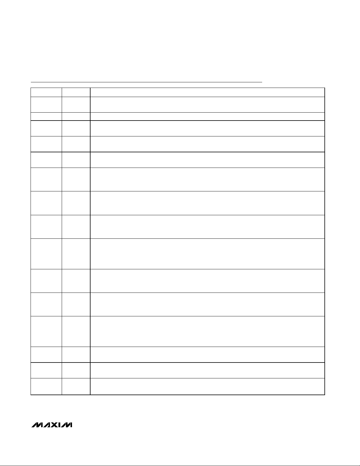
PIN NAME FUNCTION
1, 2, 3, 30,
31, 32
N.C. No Connection. Not internally connected.
4, 9, 20, 25
GND Ground
5 ENB
Channel B Output Enable. Drive ENB high to enable the LVDS outputs for channel B. An internal 435kΩ
resistor to GND pulls ENB low when unconnected.
6 OUTB
Channel B LVDS Noninverting Output. Connect a 100Ω termination resistor between OUTB and OUTB at
the receiver inputs to ensure proper operation.
7 OUTB
Channel B LVDS Inverting Output. Connect a 100Ω termination resistor between OUTB and OUTB at the
receiver inputs to ensure proper operation.
8, 13, 24,
29
V
CC
Power-Supply Input. Bypass each VCC to GND with a 0.1µF and 0.01µF ceramic capacitor. Install both
bypass capacitors as close to the device as possible, with the 0.01µF capacitor closest to the device.
10 INB0
LVDS/HSTL (MAX9394) or LVPECL/CML (MAX9395) Inverting Input. An internal 128kΩ pullup resistor to
V
CC
pulls the input high when unconnected (MAX9394). An internal 68kΩ resistor to GND pulls the input
low when unconnected (MAX9395).
11 INB0
LVDS/HSTL (MAX9394) or LVPECL/CML (MAX9395) Noninverting Input. An internal 128kΩ pullup
resistor to VCC pulls the input high when unconnected (MAX9394). An internal 68kΩ resistor to GND
pulls the input low when unconnected (MAX9395).
12
Loopback Select for Channel B Output. Connect LB_SELB to GND or leave unconnected to reproduce
the INB_ (INB_) differential inputs at OUTB (OUTB). Connect LB_SELB to V
CC
to loop back the INA (INA)
differential inputs to OUTB (OUTB). An internal 435kΩ resistor to GND pulls LB_SELB low when
unconnected.
14 INB1
LVDS/HSTL (MAX9394) or LVPECL/CML (MAX9395) Inverting Input. An internal 128kΩ pullup resistor to
V
CC
pulls the input high when unconnected (MAX9394). An internal 68kΩ resistor to GND pulls the input
low when unconnected (MAX9395).
15 INB1
LVDS/HSTL (MAX9394) or LVPECL/CML (MAX9395) Noninverting Input. An internal 128kΩ pullup
resistor to VCC pulls the input high when unconnected (MAX9394). An internal 68kΩ resistor to GND
pulls the input low when unconnected (MAX9395).
16 BSEL
Channel B Multiplexer Control Input. Selects the differential input to reproduce at the B channel
differential output. Connect BSEL to GND or leave unconnected to select the INB0 (INB0) set of inputs.
Connect BSEL to V
CC
to select the INB1 (INB1) set of inputs. An internal 435kΩ resistor to GND pulls
BSEL low when unconnected.
17 ENA1
Channel A1 Output Enable. Drive ENA1 high to enable the A1 LVDS outputs. An internal 435kΩ resistor
to GND pulls the ENA1 low when unconnected.
18
Channel A1 LVDS Inverting Output. Connect a 100Ω termination resistor between OUTA1 and OUTA1 at
the receiver inputs to ensure proper operation.
19
Channel A1 LVDS Noninverting Output. Connect a 100Ω termination resistor between OUTA1 and
OUTA1 at the receiver inputs to ensure proper operation.
LB_SELB
OUTA1
OUTA1
Page 6

MAX9394/MAX9395
2:1 Multiplexers and 1:2 Demultiplexers with
Loopback
6 _______________________________________________________________________________________
Pin Description (continued)
PIN
FUNCTION
21 ENA0
Channel A0 Output Enable. Drive ENA0 high to enable the A0 LVDS outputs. An internal 435kΩ resistor
to GND pulls ENA0 low when unconnected.
22
Channel A0 LVDS Inverting Output. Connect a 100Ω termination resistor between OUTA0 and OUTA0 at
the receiver inputs to ensure proper operation.
23
Channel A0 LVDS Noninverting Output. Connect a 100Ω termination resistor between OUTA0 and
OUTA0 at the receiver inputs to ensure proper operation.
26 INA
LVDS/HSTL (MAX9394) or LVPECL/CML (MAX9395) Noninverting Input. An internal 128kΩ pullup
resistor to V
CC
pulls the input high when unconnected (MAX9394). An internal 68kΩ resistor to GND
pulls the input low when unconnected (MAX9395).
27 INA
LVDS/HSTL (MAX9394) or LVPECL/CML (MAX9395) Inverting Input. An internal 128kΩ pullup resistor to
VCC pulls the input high when unconnected (MAX9394). An internal 68kΩ resistor to GND pulls the input
low when unconnected (MAX9395).
28
Loopback Select for Channel A Output. Connect LB_SELA to GND or leave unconnected to reproduce
the INA (INA) differential inputs at OUTA_ (OUTA_). Connect LB_SELA to V
CC
to loop back the INB_
(INB_) differential inputs to OUTA_ (OUTA_). An internal 435kΩ resistor to GND pulls LB_SELA low when
unconnected.
NAME
OUTA0
OUTA0
LB_SELA
Page 7

MAX9394/MAX9395
2:1 Multiplexers and 1:2 Demultiplexers with
Loopback
_______________________________________________________________________________________ 7
t
PHL
t
PLH
80%
20%
20%
80%
50% V
OD
= 0V
V
OD
= 0V
V
ID
= 0V
V
OD
= 0V
V
OD
= 0V
V
ID
= 0V
50%
V
ID
= V
IN_ _
- V
IN_ _
VOD = V
OUT_ _
- V
OUT_ _
V
IN_ _
V
IHD
V
ILD
V
IN_ _
V
OUT_ _
V
OUT_ _
t
F
t
R
Figure 1. Output Transition Time and Propagation Delay Timing
Diagram
VID = V
IN_ _
- V
IN_ _
ΔVOD = ⎪VOD - VOD*⎪ RL = 100Ω ±1%
ΔV
OS
= ⎪VOS - VOS*⎪
V
OD
AND V
OS
ARE MEASURED WITH VID = +100mV.
V
OD
* AND VOS* ARE MEASURED WITH VID = -100mV.
IN_ _
IN_ _
R
L
/2
RL/2
V
OD
OUT_ _
OUT_ _
MAX9394/MAX9395
EN_ _ = HIGH
V
OS
Figure 2. Test Circuit for VODand V
OS
V
IHD
V
ILD
V
IHD
V
ILD
V
IH
V
IL
t
SWITCH
t
SWITCH
INB0
INB0
INB1
INB1
V
ID
= 0V
V
ID
= 0V
BSEL
1.5V
INB1
OUT_ _
OUT_ _
EN_0 = EN_1 = HIGH
V
ID
= V
IN_ _
- V
IN_ _
INB0
INB0
1.5V
VOD = 0V
V
OD
= 0V
Figure 3. Input to Rising/Falling Edge Select and Mux Switch Timing Diagram
Page 8

MAX9394/MAX9395
2:1 Multiplexers and 1:2 Demultiplexers with
Loopback
8 _______________________________________________________________________________________
VID = V
IN_ _
- V
IN_ _
0V
3V
1.5V
1.5V
V
EN_ _
t
PHD
t
PHD
t
PDH
t
PDH
50%
50%
50%
50%
V
OUT_ _
WHEN VID = +100mV
V
OUT_ _
WHEN VID = -100mV
C
L
PULSE
GENERATOR
IN_ _
IN_ _
R
L
/2
RL/2
50Ω
OUT_ _
OUT_ _
1.25V
C
L
MAX9394/MAX9395
V
OUT_ _
WHEN VID = -100mV
V
OUT_ _
WHEN VID = +100mV
EN_ _
R
L
= 100Ω ±1%
C
L
= 1.0pF
Figure 4. Output Active-to-Disable and Disable-to-Active Test Circuit and Timing Diagram
LB_SELA
0
LB
PULSE
GENERATOR
OUTA0
OUTA0
OUTA1
OUTA1
C
L
R
L
R
L
INA
INA
50Ω
C
L
50Ω
C
L
C
L
MAX9394
MAX9395
ENA0 = ENA1 = HIGH
1 CHANNEL SHOWN.
FROM
CHANNEL B
R
L
= 100Ω ±1%
C
L
= 1.0pF
Figure 5. Output Transition Time, Propagation Delay, and Output Channel-to-Channel Skew Test Circuit
Page 9

Detailed Description
The LVDS interface standard provides a signaling
method for point-to-point communication over a controlled-impedance medium as defined by the ANSI
TIA/EIA-644 standard. LVDS utilizes a lower voltage
swing than other communication standards, achieving
higher data rates with reduced power consumption,
while reducing EMI emissions and system susceptibility
to noise.
The MAX9394/MAX9395 high-speed, low-power 2:1
multiplexers and 1:2 demultiplexers with loopback provide signal redundancy switching in telecom and storage applications. These devices select one of two
remote signal sources for local input and buffer a single
local output signal to two remote receivers.
The multiplexer section (channel B) accepts two differential inputs and generates a single LVDS output. The
demultiplexer section (channel A) accepts a single differential input and generates two parallel LVDS outputs. The
MAX9394/MAX9395 feature a loopback mode that connects the input of channel A to the output of channel B
and connects the selected input of channel B to the outputs of channel A. LB_SELA and LB_SELB provide independent loopback control for each channel.
Three LVCMOS/LVTTL logic inputs control the internal
connections between inputs and outputs, one for the
multiplexer portion of channel B (BSEL), and the other
two for loopback control of channels A and B (LB_SELA
and LB_SELB). Independent enable inputs for each differential output pair provide additional flexibility.
Input Fail-Safe
The differential inputs of the MAX9394/MAX9395 possess internal fail-safe protection. Fail-safe circuitry
forces the outputs to a differential-low condition for
undriven inputs or when the common-mode voltage
exceeds the specified range. The MAX9394 provides
high-level input fail-safe detection for LVDS, HSTL, and
other GND-referenced differential inputs. The MAX9395
provides low-level input fail-safe detection for LVPECL,
CML, and other V
CC
-referenced differential inputs.
Select Function
BSEL selects the differential input pair to transmit
through OUTB (OUTB) for LB_SELB = GND or through
OUTA_ (OUTA_) for LB_SELA = VCC. LB_SEL_ controls
the loopback function for each channel. Connect
LB_SEL_ to GND to select the normal inputs for each
channel. Connect LB_SEL_ to VCCto enable the loopback function. The loopback function routes the input of
channel A to the output of channel B, and the inputs of
channel B to the outputs of channel A. See Tables 1
and 2 for a summary of the input/output routing
between channels.
Enable Function
The EN_ _ logic inputs enable and disable each set of
differential outputs. Connect EN_ 0 to VCCto enable the
OUT_0/OUT_0 differential output pair. Connect EN_0 to
GND to disable the OUT_0/OUT_0 differential output
pair. The differential output pairs assert to a differential
low condition when disabled.
Applications Information
Differential Inputs
The MAX9394/MAX9395 inputs accept any differential
signaling standard within the specified common-mode
voltage range. The fail-safe feature detects commonmode input signal levels and generates a differential
output low condition for undriven inputs or when the
common-mode voltage exceeds the specified range
(VCM≥ VCC- 0.6V, MAX9394; VCM≤ 0.6V, MAX9395).
Leave unused inputs unconnected or connect to V
CC
for the MAX9394 or to GND for the MAX9395.
MAX9394/MAX9395
2:1 Multiplexers and 1:2 Demultiplexers with
Loopback
_______________________________________________________________________________________ 9
VOD = V
OUT_ _
- V
OUT_ _
VOD = 0V
t
CCS
VOD = 0V
V
OD
= 0V VOD = 0V
t
CCS
V
OUTA0
V
OUTA0
V
OUTA1
V
OUTA1
Figure 6. Output Channel-to-Channel Skew
Page 10

MAX9394/MAX9395
Differential Outputs
The output common-mode voltage is not properly
established if the LVDS output is higher than 0.6V when
the supply voltage is ramping up at power-on. This
condition can occur when an LVDS output drives an
LVDS input on the same chip. To avoid this situation for
the MAX9394/MAX9395, connect a 10kΩ resistor from
the noninverting output (OUT_) to ground, and connect
a 10kΩ resistor from the inverting output (OUT_) to
ground. These pulldown resistors keep the output
below 0.6V when the supply is ramping up (Figure 7).
Power-Supply Bypassing
Bypass each VCCto GND with high-frequency surfacemount ceramic 0.1µF and 0.01µF capacitors in parallel
as close to the device as possible. Install the 0.01µF
capacitor closest to the device.
Differential Traces
Input and output trace characteristics affect the performance of the MAX9394/MAX9395. Connect each input
and output to a 50Ω characteristic impedance trace.
Maintain the distance between differential traces and
eliminate sharp corners to avoid discontinuities in differential impedance and maximize common-mode
noise immunity. Minimize the number of vias on the differential input and output traces to prevent impedance
discontinuities. Reduce reflections by maintaining the
50Ω characteristic impedance through connectors and
across cables. Minimize skew by matching the electrical length of the traces.
Output Termination
Terminate LVDS outputs with a 100Ω resistor between
the differential outputs at the receiver inputs. LVDS outputs require 100Ω termination for proper operation.
Ensure that the output currents do not exceed the current limits specified in the Absolute Maximum Ratings.
Observe the total thermal limits of the MAX9394/
MAX9395 under all operating conditions.
Cables and Connectors
Use matched differential impedance for transmission
media. Use cables and connectors with matched differential impedance to minimize impedance discontinuities. Avoid the use of unbalanced cables.
Balanced cables such as twisted pair offer superior
signal quality and tend to generate less EMI due to
canceling effects.
Board Layout
Use a four-layer printed circuit (PC) board providing
separate signal, power, and ground planes for highspeed signaling applications. Bypass VCCto GND as
close to the device as possible. Install termination
resistors as close to receiver inputs as possible. Match
the electrical length of the differential traces to minimize
signal skew.
2:1 Multiplexers and 1:2 Demultiplexers with
Loopback
10 ______________________________________________________________________________________
LB_SEL_ OUT_ _
GND or open Normal inputs selected.
V
CC
Loopback inputs selected.
Table 2. Loopback Select Truth Table
LOGIC INPUTS DIFFERENTIAL OUTPUTS
LB_SELA LB_SELB BSEL OUTA_ / OUTA_ OUTB / OUTB
0 0 0 INA selected INB0 selected
0 0 1 INA selected INB1 selected
0 1 X INA selected INA selected
1 0 0 INB0 selected INB0 selected
1 0 1 INB1 selected INB1 selected
1 1 0 INB0 selected INA selected
1 1 1 INB1 selected INA selected
Table 1. Input Select Truth Table
X = Don’t care.
100Ω DIFFERENTIAL
TRANSMISSION LINE
100Ω
TERMINATION
RESISTOR
10kΩ
GND
10kΩ
OUT_
OUT_
MAX9394
MAX9395
Figure 7. Pulldown Resistor Configuration for LVDS Outputs
Page 11

MAX9394/MAX9395
2:1 Multiplexers and 1:2 Demultiplexers with
Loopback
______________________________________________________________________________________ 11
0
LB
LB
0
OUTA1
ENA1
ENA0
LB_SELA
BSEL
OUTA1
OUTA0
OUTA0
INA
INA
MAX9394
MAX9395
INB0
INB0
INB1
INB1
ENB
LB_SELB
OUTB
OUTB
1
0
Functional Diagram
Page 12

MAX9394/MAX9395
2:1 Multiplexers and 1:2 Demultiplexers with
Loopback
12 ______________________________________________________________________________________
Chip Information
TRANSISTOR COUNT: 1565
PROCESS: BIPOLAR
TOP VIEW
MAX9394
MAX9395
TQFP
32 28
293031
25
26
27
N.C.
N.C.
VCCLB_SELA
N.C.
INA
INA
GND
10
13
15
14
1611 12
9
GND
INB0
INB0
LB_SELB
V
CC
INB1
INB1
BSEL
17
18
19
20
21
22
23
OUTA0
24 V
CC
OUTA0
ENA0
GND
OUTA1
OUTA1
ENA1
2
3
4
5
6
7
8V
CC
OUTB
OUTB
GND
N.C.
N.C.
1N.C.
ENB
+
Pin Configurations
Page 13

MAX9394/MAX9395
2:1 Multiplexers and 1:2 Demultiplexers with
Loopback
______________________________________________________________________________________ 13
Package Information
(The package drawing(s) in this data sheet may not reflect the most current specifications. For the latest package outline information,
go to www.maxim-ic.com/packages.)
32L TQFP, 5x5x01.0.EPS
B
1
2
21-0110
PACKAGE OUTLINE, 32L TQFP, 5x5x1.0mm
Page 14

MAX9394/MAX9395
2:1 Multiplexers and 1:2 Demultiplexers with
Loopback
Maxim cannot assume responsibility for use of any circuitry other than circuitry entirely embodied in a Maxim product. No circuit patent licenses are
implied. Maxim reserves the right to change the circuitry and specifications without notice at any time.
14 ____________________Maxim Integrated Products, 120 San Gabriel Drive, Sunnyvale, CA 94086 408-737-7600
© 2007 Maxim Integrated Products is a registered trademark of Maxim Integrated Products, Inc.
Package Information (continued)
(The package drawing(s) in this data sheet may not reflect the most current specifications. For the latest package outline information,
go to www.maxim-ic.com/packages.)
B
2
2
21-0110
PACKAGE OUTLINE, 32L TQFP, 5x5x1.0mm
Revision History
All pages changed at Rev 1
 Loading...