

Page 1
General Description
The MAX9389 is a fully differential, high-speed, low-jitter,
8-to-1 ECL/PECL multiplexer (mux) with dual output
buffers. The device is designed for clock and data distribution applications, and features extremely low propagation delay (310ps typ) and output-to-output skew
(30ps max).
Three single-ended select inputs, SEL0, SEL1, and SEL2,
control the mux function. The mux select inputs are compatible with ECL/PECL logic, and are internally referenced to the on-chip reference output (V
BB1
, V
BB2
),
nominally VCC- 1.425V. The select inputs accept signals
between VCCand VEE. Internal pulldowns to VEEensure
a low default condition if the select inputs are left open.
The differential inputs D_, D_ can be configured to
accept a single-ended signal when the unused complementary input is connected to the on-chip reference
output (V
BB1
, V
BB2
). All the differential inputs have
internal bias and clamping circuits that ensure a low
output state when the inputs are left open.
The MAX9389 operates with a wide supply range V
CC
VEEof 2.375V to 5.5V. The device is offered in 32-pin
TQFP and thin QFN packages, and operates over the
-40°C to +85°C extended temperature range.
Applications
High-Speed Telecom and Datacom Applications
Central-Office Backplane Clock Distribution
DSLAM/DLC
Features
♦ 310ps Propagation Delay
♦ Guaranteed 2.7GHz Operating Frequency
♦ 0.3ps
RMS
Random Jitter
♦ <30ps Output-to-Output Skew
♦ -2.375V to -5.5V Supplies for Differential
LVECL/ECL
♦ +2.375V to +5.5V Supplies for Differential
LVPECL/PECL
♦ Outputs Low for Open Inputs
♦ Dual Output Buffers
♦ >2kV ESD Protection (Human Body Model)
MAX9389
Differential 8:1 ECL/PECL Multiplexer with
Dual Output Buffers
________________________________________________________________ Maxim Integrated Products 1
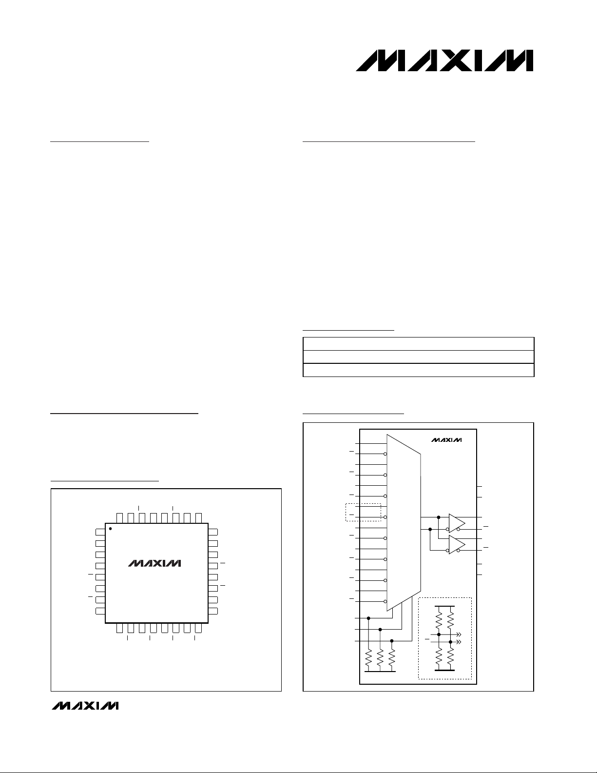
Pin Configurations
Ordering Information
V
BB1
V
BB2
V
CC
V
EE
V
CC
V
EE
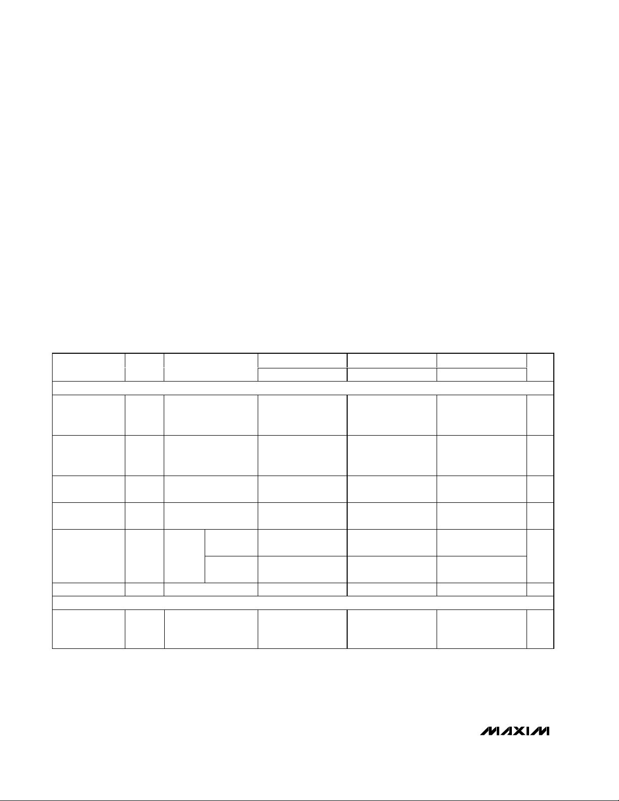
MUX
8:1
180kΩ
180kΩ165kΩ 180kΩ
232kΩ
D0
D0
D1
D1
D2
D2
D3
D3
D4
SEL0
SEL1
SEL2
D4
Q0
Q0
Q1
Q1
D_
D_
MAX9389
V
EE
D5
D5
D6
D6
D7
D7
Functional Diagram
19-2688; Rev 0; 1/03
For pricing, delivery, and ordering information, please contact Maxim/Dallas Direct! at
1-888-629-4642, or visit Maxim’s website at www.maxim-ic.com.
Pin Configurations continued at end of data sheet.
*Future product—contact factory for availability.
PART TEMP RANGE PIN-PACKAGE
MAX9389EHJ -40°C to +85°C 32 TQFP
MAX9389ETJ* -40°C to +85°C 32 Thin QFN
TOP VIEW
CC
V
BB2
V
BB1
D0
D0
D1
D1
CC
EE
Q0Q0VCCQ1
V
32 28
MAX9389
10
9
D2D3D2D4D3D5D4
TQFP
1V
2
3
4
5
6
7
8V
293031
Q1
VCCSEL2
26
25
27
24 SEL1
SEL0
23
V
22
CC
D7
14
13
21
15
D7
20
D6
19
D6
18
V
17
EE
1611 12
D5
Page 2
MAX9389
Differential 8:1 ECL/PECL Multiplexer with
Dual Output Buffers
2 _______________________________________________________________________________________
ABSOLUTE MAXIMUM RATINGS
DC ELECTRICAL CHARACTERISTICS
(VCC- VEE= 2.375V to 5.5V, outputs loaded with 50Ω±1% to VCC- 2V. Typical values are at VCC- VEE= 3.3V, V
IHD
= VCC- 1V,
V
ILD
= VCC- 1.5V, unless otherwise noted.) (Notes 1–4)
Stresses beyond those listed under “Absolute Maximum Ratings” may cause permanent damage to the device. These are stress ratings only, and functional
operation of the device at these or any other conditions beyond those indicated in the operational sections of the specifications is not implied. Exposure to
absolute maximum rating conditions for extended periods may affect device reliability.
VCC- V
EE
..............................................................-0.3V to +6.0V
Inputs (D_, D_, SEL_) to V
EE
......................-0.3V to (V
CC
+ 0.3V)
D_ to D_...............................................................................±3.0V
Continuous Output Current .................................................50mA
Surge Output Current........................................................100mA
V
BB
_ Sink/Source Current ..............................................±600µA
Continuous Power Dissipation (T
A
= +70°C)
32-Lead TQFP (derate 13.1mW/°C above +70°C) ...1047mW
θ
JA
in Still Air..........................................................+76°C/W
θ
JC
.........................................................................+25°C/W
32-Lead QFN (derate 21.3mW/°C above +70°C) .....1702mW
θ
JA
in Still Air..........................................................+47°C/W
θ
JC
...........................................................................+2°C/W
Operating Temperature Range ...........................-40°C to +85°C
Junction Temperature......................................................+150°C
Storage Temperature Range .............................-65°C to +150°C
ESD Protection
Human Body Model (D_, D_, Q_, Q_, SEL_, V
BB
_) .............≥2kV
Soldering Temperature (10s) ...........................................+300°C
PARAMETER SYMBOL CONDITIONS
INPUT (D_, D_, SEL_)
Single-Ended
Input High
Voltage
MIN TYP MAX MIN TYP MAX MIN TYP MAX
V
V
BB_
IH
unused input, Figure 1
connected to the
V
CC
1.225
-
-40°C +25°C +85°C
VCC -
V
0.880
CC
1.225
-
VCC -
0.880
V
CC
1.225
-
VCC -
0.880
UNITS
V
Single-Ended
Input Low
Voltage
Differential Input
High Voltage
Differential Input
Low Voltage
Differential Input
V
Voltage
Input Current I
OUTPUT (Q_, Q_)
Single-Ended
Output High
Voltage
V
V
V
IHD
V
V
V
connected to the
BB_
IL
unused input, Figure 1
Figure 1
IHD
Figure 1 V
ILD
V
3.0V
V
ILD
Figure 1
3.0V
V
IN
IH, VIL, VIHD, VILD
Figure 2
OH
CC
CC
- VEE <
- VEE ≥
VCC -
1.945
V
EE
1.2
EE
0.095
+
V
CC
1.625
V
CC
V
CC
0.095
V
CC
V
EE
-
-
-
VCC -
1.945
V
EE
1.2
V
EE
0.095
V
-
VCC -
CC
1.625
1.945
+
V
CC
V
CC
0.095
V
CC
V
EE
-
-
V
EE
1.2
V
EE
0.095
+
V
CC
1.625
V
CC
V
CC
0.095
V
CC
V
EE
-
-
-
0.095 3.000 0.095 3.000 0.095 3.000
-60 +60 -60 +60 -60 +60 µA
V
CC
1.145
-
V
CC
0.895
-
V
CC
1.145
-
V
CC
0.895
-
V
CC
1.145
-
V
-
CC
0.895
V
V
V
V
V
Page 3
MAX9389
Differential 8:1 ECL/PECL Multiplexer with
Dual Output Buffers
_______________________________________________________________________________________ 3
DC ELECTRICAL CHARACTERISTICS (continued)
(VCC- VEE= 2.375V to 5.5V, outputs loaded with 50Ω±1% to VCC- 2V. Typical values are at VCC- VEE= 3.3V, V
IHD
= VCC- 1V,
V
ILD
= VCC- 1.5V, unless otherwise noted.) (Notes 1–4)
AC ELECTRICAL CHARACTERISTICS
(VCC- VEE= 2.375V to 5.5V, outputs loaded with 50Ω±1% to VCC- 2V, V
IHD
- V
ILD
= 0.15V to 1V, fIN≤ 2.5GHz, input duty cycle = 50%,
input transition time = 125ps (20% to 80%). Typical values are at V
CC
- VEE= 3.3V, V
IHD
= VCC- 1V, V
ILD
= VCC- 1.5V, fIN= 622 MHz,
input duty cycle = 50%, input transition time = 125ps (20% to 80%.)) (Note 7)
PARAMETER SYMBOL CONDITIONS
Single-Ended
Output Low
V
OL
Figure 2
Voltage
Differential
Output Voltage
V
OH
V
Figure 2 650 830 650 840 650 840 mV
OL
-40°C +25°C +85°C
MIN TYP MAX MIN TYP MAX MIN TYP MAX
V
CC
1.945
-
V
CC
1.695
-
V
CC
1.945
-
V
CC
1.695
-
V
CC
1.945
-
REFERENCE OUTPUT (VBB_ )
Reference
Voltage Output
V
V
BB1
BB2
I
+ I
BB1
(Note 5)
= ±0.5mA
BB2
V
CC
1.525
-
V
CC
1.425
-
V
CC
1.325
-
V
CC
1.525
-
V
CC
1.425
-
V
CC
1.325
-
V
CC
1.525
-
V
CC
1.425
POWER SUPPLY
Supply Current I
(Note 6) 50 70 53 70 55 70 mA
EE
PARAMETER SYMBOL CONDITIONS
Differential Inputto-Output Delay
SEL_-to-Output
Delay
t
PLHD
t
PHLD
t
PLH2
t
PHL2
,
Figure 2 216 301 370 237 310 416 255 329 456 ps
Figure 4, input
,
transition time = 500ps
(20% to 80%) (Note 8)
MIN TYP MAX MIN TYP MAX MIN TYP MAX
-40°C +25°C +85°C
1.34 2 1.25 2 1.44 2 ns
-
V
CC
1.695
V
CC
1.325
UNITS
V
V
UNITS
Output-to-Output
Skew
Input-to-Output
Skew
Part-to-Part
Skew
Added Random
Jitter (Note 12)
Added
Deterministic
Jitter (Note 12)
t
SKOO
t
t
SKPP
Figure 5 (Note 9) 15 15 30 ps
Figure 6 (Note 10) 50 50 55 ps
SKIO
(Note 11) 125 150 160 ps
Clock
t
RJ
pattern
PRBS
T
DJ
2
fIN = 156MHz 0.3 1.15 0.3 1.15 0.3 1.15
fIN = 622MHz 0.3 1.15 0.3 1.15 0.3 1.15
f
= 2.5GHz 0.3 1.15 0.3 1.15 0.3 1.15
IN
fIN = 156Mbps 33 95 33 95 33 95
23
- 1
f
= 622Mbps 21 61 21 61 21 61
IN
ps
ps
RMS
P-P
Page 4

MAX9389
Differential 8:1 ECL/PECL Multiplexer with
Dual Output Buffers
4 _______________________________________________________________________________________
AC ELECTRICAL CHARACTERISTICS (continued)
(VCC- VEE= 2.375V to 5.5V, outputs loaded with 50Ω±1% to VCC- 2V, V
IHD
- V
ILD
= 0.15V to 1V, fIN≤ 2.5GHz, input duty cycle = 50%,
input transition time = 125ps (20% to 80%). Typical values are at V
CC
- VEE= 3.3V, V
IHD
= VCC- 1V, V
ILD
= VCC- 1.5V, fIN= 622 MHz,
input duty cycle = 50%, input transition time = 125ps (20% to 80%.)) (Note 7)
Note 1: Measurements are made with the device in thermal equilibrium.
Note 2: Current into an I/O pin is defined as positive. Current out of an I/O pin is defined as negative.
Note 3: DC parameters production tested at T
A
= +25°C and guaranteed by design over the full operating temperature range.
Note 4: Single-ended data input operation using V
BB
_ is limited to (VCC- VEE) ≥ 3.0V.
Note 5: Use V
BB_
only for inputs that are on the same device as the V
BB_
reference.
Note 6: All pins open except V
CC
and VEE.
Note 7: Guaranteed by design and characterization. Limits are set at ±6 sigma.
Note 8: Measured from the 50% point of the input signal with the 50% point equal to V
BB
, to the 50% point of the output signal.
Note 9: Measured between outputs of the same part at the signal crossing points for a same-edge transition.
Note 10:Measured between input-to-output paths of the same part at the signal crossing points for a same-edge transition of the
differential input signal.
Note 11:Measured between outputs of different parts at the signal crossing points under identical conditions for a same-edge
transition.
Note 12:Device jitter added to the differential input signal.
SUPPLY CURRENT vs. TEMPERATURE
MAX9389 toc01
TEMPERATURE (°C)
SUPPLY CURRENT (mA)
6035-15 10
42.5
45.0
47.5
50.0
52.5
55.0
57.5
60.0
40.0
-40 85
ALL PINS ARE OPEN EXCEPT VCC AND V
EE
DIFFERENTIAL OUTPUT VOLTAGE (VOH - VOL)
vs. FREQUENCY
MAX9389 toc02
FREQUENCY (GHz)
DIFFERENTIAL OUTPUT VOLTAGE (mV)
2.52.01.51.00.5
300
400
500
600
700
800
900
200
0 3.0
OUTPUT RISE/FALL TIME
vs. TEMPERATURE
MAX9389 toc03
RISE/FALL TIME (ps)
100
110
120
130
140
150
90
TEMPERATURE (°C)
603510-15-40
RISE
FALL
85
Typical Operating Characteristics
(VCC- VEE= 3.3V, V
IHD
= VCC- 1V, V
ILD
= VCC- 1.5V, outputs loaded with 50Ω±1% to VCC- 2V, f
IN
= 622MHz, input duty cycle = 50%,
input transition time = 125ps (20% to 80%), unless otherwise noted.)
PARAMETER SYMBOL CONDITIONS
Switching
Frequency
Select Toggle
Frequency
f
MAX
f
VOH - VOL ≥ 300mV,
Figure 2
VOH - VOL ≥ 300mV,
SEL
Figure 4
MIN TYP MAX MIN TYP MAX MIN TYP MAX
2.7 2.7 2.7 GHz
100 100 100 MHz
-40°C +25°C +85°C
Output Rise and
Fall Time
t
, tFFigure 2 67 105 138 74 117 155 81 128 165 ps
R
(20% to 80%)
UNITS
Page 5

MAX9389
Differential 8:1 ECL/PECL Multiplexer with
Dual Output Buffers
_______________________________________________________________________________________ 5
Typical Operating Characteristics (continued)
(VCC- VEE= 3.3V, V
IHD
= VCC- 1V, V
ILD
= VCC- 1.5V, outputs loaded with 50Ω±1% to VCC- 2V, f
IN
= 622MHz, input duty cycle = 50%,
input transition time = 125ps (20% to 80%), unless otherwise noted.)
Pin Description
PIN NAME FUNCTION
1, 8, 22,
26, 29
2V
PROPAGATION DELAY vs. HIGH VOLTAGE
OF DIFFERENTIAL INPUT (V
340
324
308
292
PROPAGATION DELAY (ps)
276
260
1.2 3.3
V
CC
Positive Supply Input. Bypass each VCC to VEE with 0.1µF and 0.01µF ceramic capacitors. Place the
capacitors as close to the device as possible with the smaller value capacitor closest to the device.
V
V
(V)
IHD
Reference Output Voltage 2. Connect to the inverting or noninverting data input to provide a
BB2
reference for single-ended operation. When used, bypass V
capacitor. Otherwise leave open.
)
IHD
- V
= 150mV
IHD
ILD
MAX9389 toc04
3.02.72.42.11.81.5
PROPAGATION DELAY vs. TEMPERATURE
350
330
310
290
PROPAGATION DELAY (ps)
270
250
-40
t
PHL
t
PLH
TEMPERATURE (°C)
BB2
MAX9389 toc05
603510-15
85
to VCC with a 0.01µF ceramic
Reference Output Voltage 1. Connect to the inverting or noninverting data input to provide a
3V
BB1
reference for single-ended operation. When used, bypass V
to VCC with a 0.01µF ceramic
BB1
capacitor. Otherwise leave open.
4 D0 Noninverting Differential Input 0. Internal 232kΩ to VCC and 180kΩ to VEE.
5 D0 Inverting Differential Input 0. Internal 180kΩ to VCC and 180kΩ to VEE.
6 D1 Noninverting Differential Input 1. Internal 232kΩ to VCC and 180kΩ to VEE.
7 D1 Inverting Differential Input 1. Internal 180kΩ to VCC and 180kΩ to VEE.
9 D2 Noninverting Differential Input 2. Internal 232kΩ to VCC and 180kΩ to VEE.
10 D2 Inverting Differential Input 2. Internal 180kΩ to VCC and 180kΩ to VEE.
11 D3 Noninverting Differential Input 3. Internal 232kΩ to VCC and 180kΩ to VEE.
12 D3 Inverting Differential Input 3. Internal 180kΩ to VCC and 180kΩ to VEE.
13 D4 Noninverting Differential Input 4. Internal 232kΩ to V
and 180kΩ to VEE.
CC
14 D4 Inverting Differential Input 4. Internal 180kΩ to VCC and 180kΩ to VEE.
15 D5 Noninverting Differential Input 5. Internal 232kΩ to VCC and 180kΩ to VEE.
16 D5 Inverting Differential Input 5. Internal 180kΩ to VCC and 180kΩ to VEE.
17, 32 V
EE
Negative Supply Input
18 D6 Noninverting Differential Input 6. Internal 232kΩ to VCC and 180kΩ to VEE.
19 D6 Inverting Differential Input 6. Internal 180kΩ to VCC and 180kΩ to VEE.
Page 6

MAX9389
Differential 8:1 ECL/PECL Multiplexer with
Dual Output Buffers
6 _______________________________________________________________________________________
Pin Description (continued)
Figure 1. Input Definitions
Figure 2. Differential Input-to-Output Propagation Delay Timing
Diagram
Figure 3. Single-Ended Input-to-Output Propagation Delay
Timing Diagram
Figure 4. Select Input (SEL0) to Output (Q_, Q_) Delay Timing
Diagram
PIN NAME FUNCTION
20 D7 Noninverting Differential Input 7. Internal 232kΩ to VCC and 180kΩ to VEE.
21 D7 Inverting Differential Input 7. Internal 180kΩ to VCC and 180kΩ to VEE.
23 SEL0 Select Logic Input 0. Internal 165kΩ pulldown to VEE.
24 SEL1 Select Logic Input 1. Internal 165kΩ pulldown to VEE.
25 SEL2 Select Logic Input 2. Internal 165kΩ pulldown to VEE.
27 Q1 Inverting Output 1. Typically terminate with 50Ω resistor to VCC - 2V.
28 Q1 Noninverting Output 1. Typically terminate with 50Ω resistor to VCC - 2V.
30 Q0 Inverting Output 0. Typically terminate with 50Ω resistor to VCC - 2V.
31 Q0 Noninverting Output 0. Typically terminate with 50Ω resistor to VCC - 2V.
— EP Exposed Pad (QFN Package Only). Connect to VEE.
V
CC
V
- V
IHD
ILD
- V
V
IHD
ILD
V
EE
DIFFERENTIAL INPUT VOLTAGE DEFINITION
V
D_
V
- V
IHD
V
V
IHD
V
ILD
V
IHD
V
ILD
CC
(MAX)
(MAX)
V
BB
(MIN)
(MIN)
V
EE
SINGLE-ENDED INPUT VOLTAGE DEFINITION
V
IH
V
IL
D_
Q_
Q_
DIFFERENTIAL OUTPUT
WAVEFORM
Q_ - Q_
20%
t
PLHD
80%
ILD
t
PHLD
VOH - V
OL
VOH - V
OL
VOH - V
OL
t
R
80%
t
F
IHD
V
ILD
V
OH
V
OL
0V (DIFFERENTIAL)
20%
D_, D1
V
- V
IHD
ILD
D_, D1
SEL_ = VIL OR OPEN
SELO
Q_
Q_
t
PLH2
VOH - V
OL
D_ WHEN D_ = V
D_ WHEN D_ = V
BB
OR
BB
Q_
Q_
t
PLH1
VOH - V
V
BB
V
BB
t
PHL1
OL
V
IH
V
IL
V
OH
V
OL
t
V
PHL2
V
IHD
V
ILD
V
IH
BB
V
IL
V
OH
V
OL
Page 7

Detailed Description
The MAX9389 is a fully differential, high-speed, low-jitter
8-to-1 ECL/PECL mux with dual output buffers. The
device is designed for clock and data distribution applications, and features extremely low propagation delay
(310ps typ) and output-to-output skew (30ps max).
Three single-ended select inputs, SEL0, SEL1, and
SEL2, control the mux function (see Table 1). The mux
select inputs are compatible with ECL/PECL logic, and
are internally referenced to the on-chip reference output
(V
BB1
, V
BB2
), nominally VCC- 1.425V. The select inputs
accept signals between VCCand VEE. Internal 165kΩ
pulldowns to VEEensure a low default condition if the
select inputs are left open. Leaving SEL0, SEL1, and
SEL2 open selects the D0, D0 inputs by default.
The differential inputs D_, D_ can be configured to
accept a single-ended signal when the unused complementary input is connected to the on-chip reference
voltage (V
BB1
, V
BB2).
Voltage reference outputs V
BB1
and V
BB2
provide the reference voltage needed for single-ended operations. A single-ended input of at least
VBB_ ±100mV or a differential input of at least 100mV
switches the outputs to the VOHand VOLlevels specified in the DC Electrical Characteristics table. The maximum magnitude of the differential input from D_ to D_ is
±3.0V. This limit also applies to the difference between a
single-ended input and any reference voltage input.
*Default output when SEL0, SEL1, and SEL2 are left open.
Single-Ended Operation
The recommended supply voltage for single-ended
operation is 3.0V to 3.8V. The differential inputs (D_,
D_) can be configured to accept single-ended inputs
when operating at supply voltages greater than 2.725V.
In single-ended mode operation, the unused complementary input needs to be connected to the on-chip
reference voltage, V
BB1
or V
BB2
, as a reference. For
example, the differential D_, D_ inputs are converted to
a noninverting, single-ended input by connecting V
BB1
or V
BB2
to D_ and connecting the single-ended input to
D_. Similarly, an inverting input is obtained by connecting V
BB1
or V
BB2
to D_ and connecting the single-
ended input to D_. The single-ended input can be
driven to VCCor VEEor with a single-ended
LVPECL/LVECL signal.
MAX9389
Differential 8:1 ECL/PECL Multiplexer with
Dual Output Buffers
_______________________________________________________________________________________ 7
Figure 5. Output-to-Output Skew (t
SKOO
) Definition
Figure 6. Input-to-Output Skew (t
SKIO
) Definition
Table 1. Mux Select Input Truth Table
Q0
Q0
Q1
Q1
t
SKOO
t
SKOO
D0
D0
Q0
Q0
*t
t
PLHD
D1–D7
D1–D7
Q0
Q0
t
** t
PLHD
= | t
* - t
t
SKIO
PLHD
DATA
OUTPUT
D0* L or open L or open L or open
D1 H L or open L or open
D2 L or open H L or open
D3 H H L or open
D4 L or open L or open H
D5 H L or open H
D6 L or open H H
D7 H H H
** | OR | t
PLHD
SEL0 SEL1 SEL2
PHLD
* - t
PHLD
** |
PHLD
PHLD
*
**
Page 8

MAX9389
In single-ended operation, ensure that the supply voltage (VCC-VEE) is greater than 2.725V. The input high
minimum level must be at least (VEE+ 1.2V) or higher
for proper operation. The reference voltage VBBmust
be at least (VEE+ 1.2V) because it becomes the highlevel input when a single-ended input swings below it.
The minimum VBBoutput for the MAX9389 is (VCC-
1.525V). Substituting the minimum VBBoutput for (V
BB
= VEE+ 1.2V) results in a minimum supply (V
CC
- VEE)
of 2.725V. Rounding up to standard supplies gives the
recommended single-ended operating supply ranges
(VCC- VEE) of 3.0V to 5.5V.
When using the VBBreference output, bypass it with a
0.01µF ceramic capacitor to VCC. If VBBis not being
used, leave it unconnected. The VBBreference can
source or sink a total of 0.5mA (shared between V
BB1
and V
BB2
), which is sufficient to drive eight inputs.
Applications Information
Output Termination
Terminate each output with a 50Ω to VCC- 2V or use an
equivalent Thevenin termination. Terminate each Q_
and Q_ output with identical termination for minimal dis-
tortion. When a single-ended signal is taken from the
differential output, terminate both Q_ and Q_.
Ensure that the output current does not exceed the current limits specified in the Absolute Maximum Ratings
table. Under all operating conditions, the device’s total
thermal limits should not be exceeded.
Supply Bypassing
Bypass each VCCto V
EE
with high-frequency surfacemount ceramic 0.1µF and 0.01µF capacitors. For PECL,
bypass each VCCto VEE. For ECL, bypass each VEEto
VCC. Place the capacitors as close to the device as possible with the 0.01µF capacitor closest to the device pins.
Use multiple vias when connecting the bypass capacitors
to ground. When using the V
BB1
or V
BB2
reference outputs, bypass each one with a 0.01µF ceramic capacitor
to VCC. If the V
BB1
or V
BB2
reference outputs are not
used, they can be left open.
Traces
Circuit board trace layout is very important to maintain the
signal integrity of high-speed differential signals.
Maintaining integrity is accomplished in part by reducing
signal reflections and skew, and increasing commonmode noise immunity.
Signal reflections are caused by discontinuities in the
50Ω characteristic impedance of the traces. Avoid
discontinuities by maintaining the distance between
differential traces, not using sharp corners or using
vias. Maintaining distance between the traces also
increases common-mode noise immunity. Reducing
signal skew is accomplished by matching the electrical
length of the differential traces.
Chip Information
TRANSISTOR COUNT: 716
PROCESS: Bipolar
Differential 8:1 ECL/PECL Multiplexer with
Dual Output Buffers
8 _______________________________________________________________________________________
Pin Configurations (continued)
TOP VIEW
CC
V
BB2
V
BB1
D0
D0
D1
D1
V
CC
NOTE: VEE IS CONNECTED
TO THE UNDERSIDE
METAL SLUG.
EE
Q0Q0VCCQ1
V
32313029282726
1V
2
3
4
5
6
7
8
9
1011121314
D2
D2
MAX9389
D3
D3
D4
THIN QFN
CC
Q1
V
25 SEL2
24 SEL1
SEL0
23
V
22
CC
21
D7
20
D7
19
D6
D6
18
17
V
EE
16D5
15
D4
D5
Page 9

MAX9389
Differential 8:1 ECL/PECL Multiplexer with
Dual Output Buffers
_______________________________________________________________________________________ 9
Package Information
(The package drawing(s) in this data sheet may not reflect the most current specifications. For the latest package outline information,
go to www.maxim-ic.com/packages.)
32L TQFP, 5x5x01.0.EPS
Page 10

MAX9389
Differential 8:1 ECL/PECL Multiplexer with
Dual Output Buffers
Maxim cannot assume responsibility for use of any circuitry other than circuitry entirely embodied in a Maxim product. No circuit patent licenses are
implied. Maxim reserves the right to change the circuitry and specifications without notice at any time.
10 ____________________Maxim Integrated Products, 120 San Gabriel Drive, Sunnyvale, CA 94086 408-737-7600
© 2003 Maxim Integrated Products Printed USA is a registered trademark of Maxim Integrated Products.
Package Information (continued)
(The package drawing(s) in this data sheet may not reflect the most current specifications. For the latest package outline information,
go to www.maxim-ic.com/packages.)
D2
k
e
(ND-1) X e
L
b
0.10 M
PIN # 1 I.D.
0.35x45
E2/2
L
C A B
QFN THIN.EPS
C
E2
L
k
CC
L
C
L
D2/2
PIN # 1
I.D.
D
0.15 C A
D/2
0.15
C B
E/2
E
(NE-1) X e
DETAIL A
0.10
C
A
0.08 C
C
A3
A1
COMMON DIMENSIONS
NOTES:
1. DIMENSIONING & TOLERANCING CONFORM TO ASME Y14.5M-1994.
2. ALL DIMENSIONS ARE IN MILLIMETERS. ANGLES ARE IN DEGREES.
3. N IS THE TOTAL NUMBER OF TERMINALS.
4. THE TERMINAL #1 IDENTIFIER AND TERMINAL NUMBERING CONVENTION SHALL CONFORM TO JESD 95-1
SPP-012. DETAILS OF TERMINAL #1 IDENTIFIER ARE OPTIONAL, BUT MUST BE LOCATED WITHIN THE
ZONE INDICATED. THE TERMINAL #1 IDENTIFIER MAY BE EITHER A MOLD OR MARKED FEATURE.
5. DIMENSION b APPLIES TO METALLIZED TERMINAL AND IS MEASURED BETWEEN 0.25 mm AND 0.30 mm
FROM TERMINAL TIP.
6. ND AND NE REFER TO THE NUMBER OF TERMINALS ON EACH D AND E SIDE RESPECTIVELY.
7. DEPOPULATION IS POSSIBLE IN A SYMMETRICAL FASHION.
8. COPLANARITY APPLIES TO THE EXPOSED HEAT SINK SLUG AS WELL AS THE TERMINALS.
9. DRAWING CONFORMS TO JEDEC MO220.
10. WARPAGE SHALL NOT EXCEED 0.10 mm.
L
e e
PROPRIETARY INFORMATION
TITLE:
PACKAGE OUTLINE
16, 20, 28, 32L, QFN THIN, 5x5x0.8 mm
APPROVAL
EXPOSED PAD VARIATIONS
PROPRIETARY INFORMATION
TITLE:
PACKAGE OUTLINE
16, 20, 28, 32L, QFN THIN, 5x5x0.8 mm
DOCUMENT CONTROL NO.
21-0140
21-0140
L
REV.
1
C
2
REV.DOCUMENT CONTROL NO.APPROVAL
2
C
2
 Loading...