

Page 1
General Description
The MAX9384 fully differential dual 2:1 multiplexer
(mux) features extremely low propagation delay (560ps
max) and output-to-output skew (40ps max). The
device is ideal for clock and data multiplexing applications. The two 2:1 muxes are controlled individually or
simultaneously through mux select inputs COM_SEL,
SEL0, and SEL1. The mux select inputs are compatible
with ECL/PECL logic, and are referenced to on-chip
outputs V
BB0
and V
BB1
, nominally VCC- 1.33V.
The differential inputs D, D can be configured to accept
a single-ended signal when the unused complementary
input is connected to the on-chip supply output VBBas
a reference voltage. All the differential inputs have bias
and clamp circuits that force the outputs to a low
default when the inputs are left open or at VEE. The single-ended mux select inputs have pulldowns to VEE,
providing low default inputs when the select inputs are
left open.
The device operates with a wide supply range (VCCVEE) of +3.0V to +5.5V for PECL or -3.0V to -5.5V for
ECL, and is pin compatible with the MC100LVEL56 and
MC100EL56. The MAX9384 is offered in a 20-pin wide
SO package, and is specified for operation from -40°C
to +85°C.
Applications
High-Speed Telecom, Datacom Applications
Central-Office Backplane Clock Distribution
Access Multiplexers (DSLAM/DLC)
Features
♦ 40ps
P-P
Deterministic Jitter
♦ 440ps Differential Propagation Delay
♦ 12ps Output-to-Output Skew
♦ Individual and Common Select
♦ +3.0V to +5.5V Supplies for Differential
LVPECL/PECL
♦ -3.0V to -5.5V Supplies for Differential LVECL/ECL
♦ Outputs Low for Inputs Open or at V
EE
♦ >2kV ESD Protection (Human Body Model)
♦ Pin Compatible with MC100LVEL56 and
MC100EL56
MAX9384
ECL/PECL Dual Differential 2:1 Multiplexer
________________________________________________________________ Maxim Integrated Products 1
Ordering Information
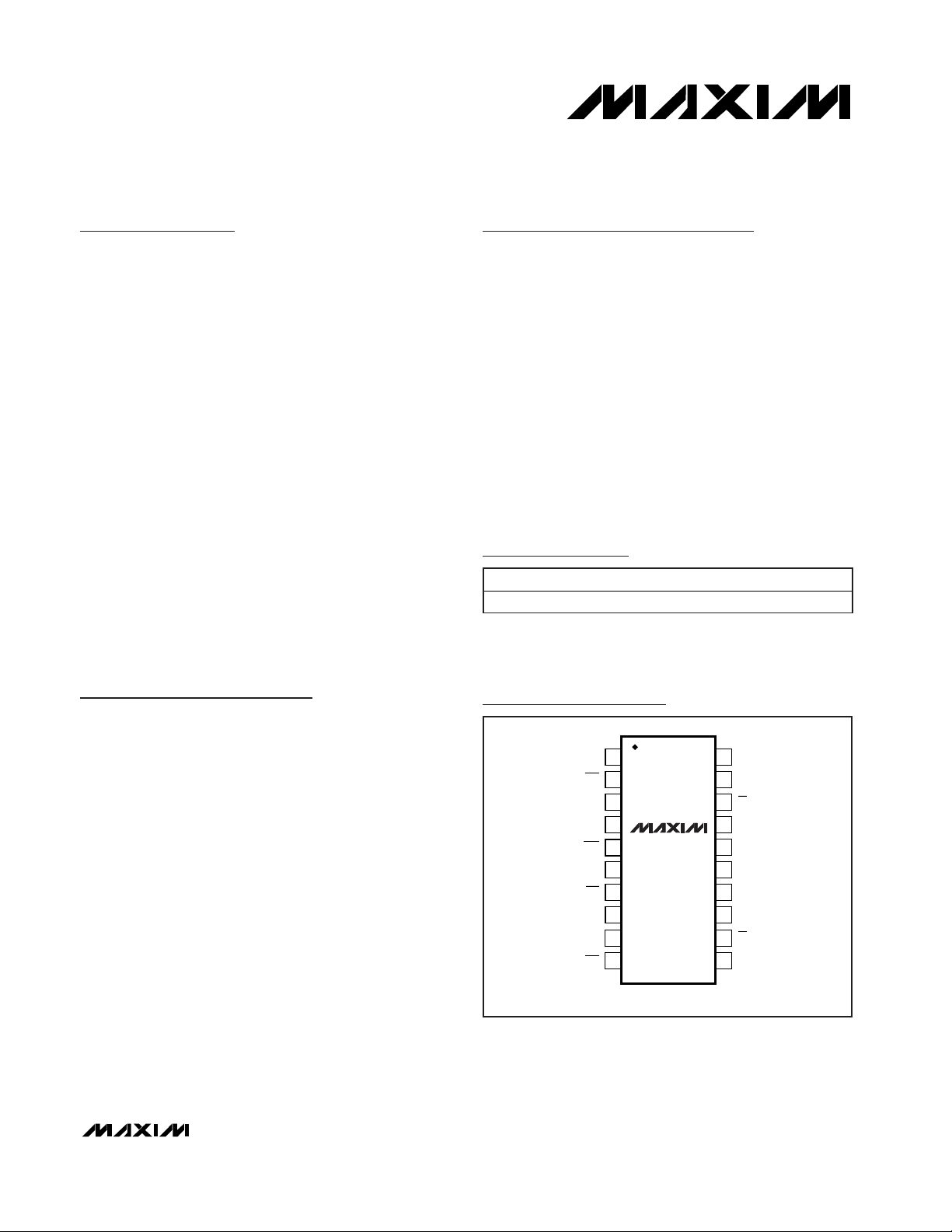
20
19
18
17
16
15
14
13
1
2
3
4
5
6
7
8
V
CC
SEL0D0b
V
BB0
V
BB1
D0a
TOP VIEW
COM_SEL
SEL1
V
CC
Q1
D1a
D1b
12
11
9
10 V
EE
MAX9384
SO
DOa
DOb
D1a
D1b
Q1
Q0
Q0
Pin Configuration
19-2484; Rev 0; 7/02
For pricing, delivery, and ordering information, please contact Maxim/Dallas Direct! at
1-888-629-4642, or visit Maxim’s website at www.maxim-ic.com.
Functional Diagram appears at end of data sheet.
PART TEMP RANGE PIN-PACKAGE
MAX9384EWP -40°C to +85°C 20 Wide SO
Page 2
MAX9384
ECL/PECL Dual Differential 2:1 Multiplexer
2 _______________________________________________________________________________________
ABSOLUTE MAXIMUM RATINGS
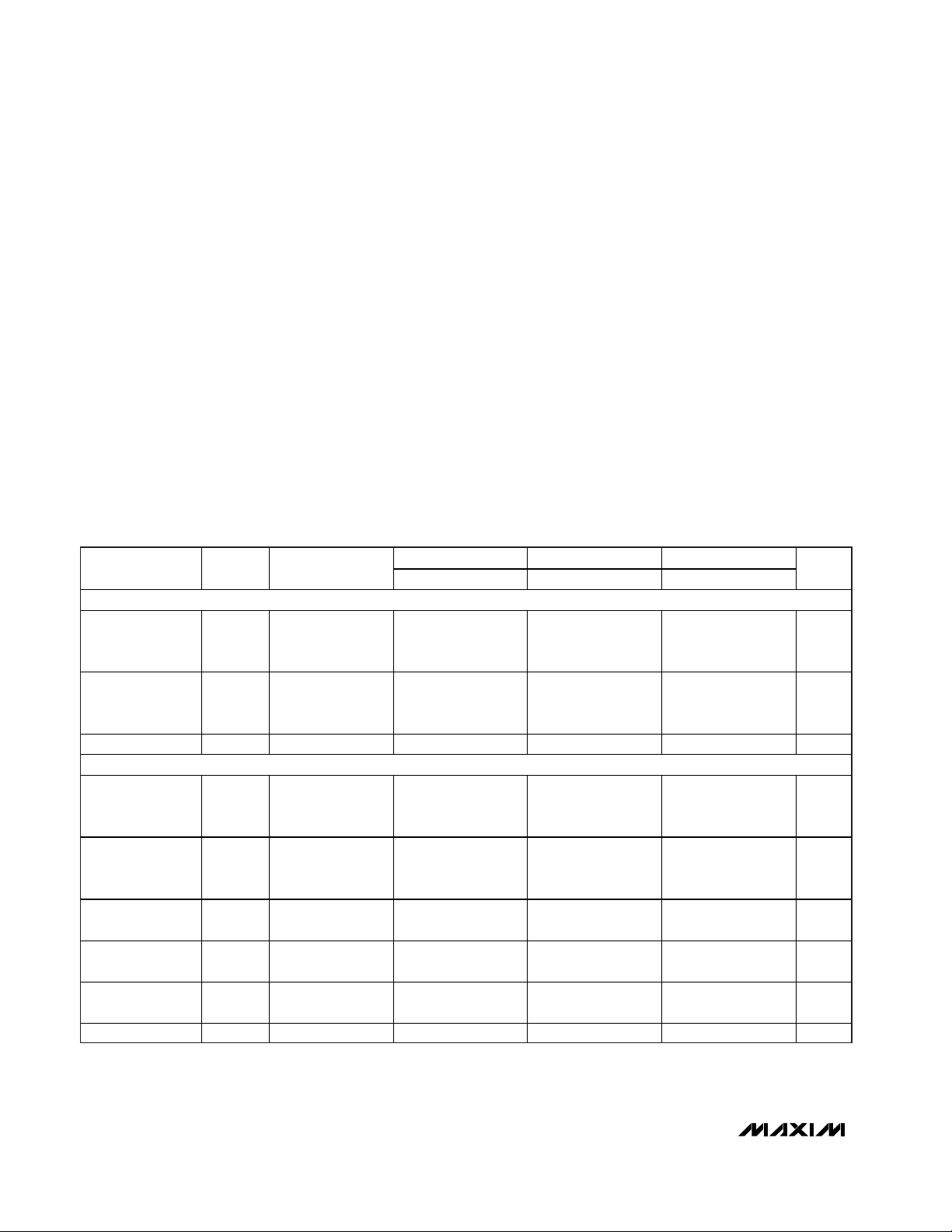
DC ELECTRICAL CHARACTERISTICS
(VCC- VEE= 3.0V to 5.5V, outputs loaded with 50Ω ±1% to VCC- 2V. Typical values are at VCC- VEE= 3.3V, V
IHD
= VCC- 1V, V
ILD
=
V
CC
- 1.5V, unless otherwise noted.) (Notes 1, 2, 3)
Stresses beyond those listed under “Absolute Maximum Ratings” may cause permanent damage to the device. These are stress ratings only, and functional
operation of the device at these or any other conditions beyond those indicated in the operational sections of the specifications is not implied. Exposure to
absolute maximum rating conditions for extended periods may affect device reliability.
VCC- VEE.................................................................-0.3V to 6.0V
Inputs (D_, D_, SEL_, COM_SEL) to V
EE
....-0.3V to (VCC+ 0.3V)
D_ to D_ ..............................................................................±3.0V
Continuous Output Current .................................................50mA
Surge Output Current........................................................100mA
V
BB
Sink/Source Current ...............................................±0.65mA
Junction-to-Ambient Thermal Resistance in Still Air
20-Lead Wide SO ....................................................+100°C/W
Junction-to-Ambient Thermal Resistance with
500LFPM Airflow
20-Lead Wide SO ......................................................+58°C/W
Junction-to-Case Thermal Resistance
20-Lead Wide SO ......................................................+20°C/W
Continuous Power Dissipation (T
A
= +70°C)
20-Lead Wide SO
(derate 10mW/°C above +70°C)..................................800mW
Operating Temperature Range ...........................-40°C to +85°C
Junction Temperature......................................................+150°C
Storage Temperature Range .............................-65°C to +150°C
ESD Protection
Human Body Model
(D_, D_, Q_, Q_, SEL_, COM_SEL) .................................≥ 2kV
Soldering Temperature (10s) ...........................................+300°C
-40°C +25°C +85°C
PARAMETER
SYMBOL
CONDITIONS
UNITS
SINGLE-ENDED INPUT SEL_, COM_SEL
Input High
Voltage
V
IH
Internally
referenced to
V
BB
, Figure 1
V
CC
-
VCC -
VCC -
V
Input Low
Voltage
V
IL
Internally
referenced to
V
BB
, Figure 1
V
CC
-
VCC -
VCC -
VCC -
VCC -
VCC -
V
Input Current I
IN
VIH, V
IL
µA
DIFFERENTIAL INPUT (D_, D_)
Single-Ended
Input High
Voltage
V
IH
VBB connected to
the unused input,
Figure 1
V
CC
-
VCC -
VCC -
V
Single-Ended
Input Low
Voltage
V
IL
VBB connected to
the unused input,
Figure 1
V
CC
-
VCC -
VCC -
VCC -
VCC -
VCC -
V
High Voltage of
Differential Input
V
IHD
Figure 1
V
EE
+
VEE +
VEE +
V
Low Voltage of
Differential Input
V
ILD
Figure 1
VCC -
VCC -
VCC -
V
Differential Input
Voltage
V
IHD
-
V
ILD
Figure 1
V
Input Current I
IN
µA
MIN TYP MAX MIN TYP MAX MIN TYP MAX
VIH, VIL, V
V
1.165
1.810
-10 +50 -10 +50 -10 +50
1.165
1.810
1.3
V
EE
CC
1.475
V
CC
1.475
V
CC
0.095
1.165
1.810
1.165
1.810
1.2
V
EE
0.095 3.0 0.095 3.0 0.095 3.0
IHD
, V
-100 +100 -100 +100 -100 +100
ILD
V
CC
1.475
V
CC
1.475
V
CC
0.095
1.165
1.810
1.165
1.810
1.2
V
EE
V
CC
1.475
V
CC
1.475
V
CC
0.095
Page 3
MAX9384
ECL/PECL Dual Differential 2:1 Multiplexer
_______________________________________________________________________________________ 3
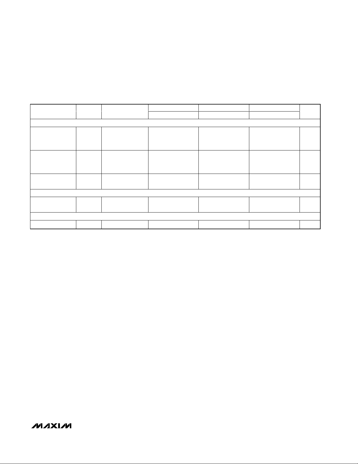
DC ELECTRICAL CHARACTERISTICS (continued)
(VCC- VEE= 3.0V to 5.5V, outputs loaded with 50Ω ±1% to VCC- 2V. Typical values are at VCC- VEE= 3.3V, V
IHD
= VCC- 1V, V
ILD
=
V
CC
- 1.5V, unless otherwise noted.) (Notes 1, 2, 3)
-40°C +25°C +85°C
PARAMETER
SYMBOL
CONDITIONS
UNITS
OUTPUT (Q_, Q_)
Single-Ended
Output High
Voltage
V
OH
Figure 2
V
CC
-
VCC -
VCC -
VCC -
VCC -
VCC -
VCC -
VCC -
VCC -
V
Single-Ended
Output Low
Voltage
V
OL
Figure 2
V
CC
-
VCC -
VCC -
VCC -
VCC -
VCC -
VCC -
VCC -
VCC -
V
Differential
Output Voltage
VOH -
V
OL
Figure 2
mV
REFERENCE OUTPUT (VBB)
Reference
Voltage Output
V
BB
IBB = ±0.5mA
(Note 4)
VCC -
VCC -
VCC -
VCC -
VCC -
VCC -
VCC -
VCC -
VCC -
V
SUPPLY
Supply Current I
EE
(Note 5)
mA
MIN TYP MAX MIN TYP MAX MIN TYP MAX
1.085
0.998
0.880
1.025
0.947
0.880
1.025
1.830
1.707
1.555
1.810
1.685
1.620
1.810
600 640 660
1.38
1.322
1.26
1.38
1.330
15 24 17 24 19 24
1.26
1.38
0.929
1.690
1.335
0.880
1.620
1.26
Page 4

MAX9384
ECL/PECL Dual Differential 2:1 Multiplexer
4 _______________________________________________________________________________________
Note 1: Measurements are made with the device in thermal equilibrium.
Note 2: Current into a pin is defined as positive. Current out of a pin is defined as negative.
Note 3: DC parameters production tested at T
A
= +25°C and guaranteed by design over the full operating temperature range.
Note 4: Use V
BB
only for inputs that are on the same device as the VBBreference.
Note 5: All pins open except V
CC
and VEE.
Note 6: Guaranteed by design and characterization. Limits are set at ±6 sigma.
Note 7: Test conditions are V
IH
= VCC- 1.11V and VIL= VCC- 1.53V.
Note 8: Measured between outputs of the same part at the signal crossing points for a same-edge transition. Differential input signal.
Note 9: Device jitter added to the input signal. Differential input signal.
-40°C +25°C +85°C
PARAMETER
CONDITIONS
UNITS
Differential
Input-to-Output
Delay
t
PLHD
,
t
PHLD
Figure 2
ps
Single-Ended
Input-to-Output
Delay
t
PLH1
,
t
PHL1
Figure 3 (Note 7)
ps
SEL_ and
COM_SEL to
Output Delay
t
PLH2
,
t
PHL2
Figure 4 (Note 7)
ps
Output-to-Output
Skew
(Note 8)
ps
Added Random
Jitter
t
RJ
fIN = 500MHz
(Note 9)
ps
(RMS
)
Added
Deterministic
Jitter
t
DJ
1.0Gbps 223 - 1
PRBS pattern
(Note 9)
ps
(P-P)
Switching
Frequency
f
MAX
VOH - VOL ≥
300mV, Figure 2
GHz
Output Rise and
Fall Time
(20% to 80%)
t
R
, t
F
Figure 2
ps
AC ELECTRICAL CHARACTERISTICS
(VCC- VEE= 3.0V to 5.5V, outputs loaded with 50Ω ±1% to VCC- 2V, V
IHD
- V
ILD
= 0.15V to 1V, fIN≤ 500MHz, input duty cycle = 50%,
input transition time = 125ps (20% to 80%). Typical values are at V
CC
- VEE= 3.3V, V
IHD
= VCC- 1V, V
ILD
= VCC- 1.5V, unless other-
wise noted.) (Note 6)
SYMBOL
MIN TYP MAX MIN TYP MAX MIN TYP MAX
340 540 350 550 360 560
290 540 310 560 330 580
310 730 320 740 330 750
t
SKOO
1.5 1.5 1.5
200 310 440 200 310 440 200 310 440
12 40 12 40 12 40
0.3 0.8 0.4 0.8 0.5 0.8
40 70 40 70 40 70
Page 5

MAX9384
ECL/PECL Dual Differential 2:1 Multiplexer
_______________________________________________________________________________________ 5
DIFFERENTIAL OUTPUT EYE PATTERN AT
500Mbps, PRBS 2
23
- 1, NRZ DATA PATTERN
MAX9384 toc02
300ps/div
Q_ - Q_
200mV/div
DIFFERENTIAL OUTPUT EYE PATTERN AT
1Gbps, PRBS 2
23
- 1, NRZ DATA PATTERN
MAX9384 toc01
200ps/div
Q_ - Q_
200mV/div
SUPPLY CURRENT (IEE)
vs. TEMPERATURE
MAX9384 toc03
TEMPERATURE (°C)
SUPPLY CURRENT (mA)
603510-15
12.5
15.0
17.5
20.0
22.5
25.0
10.0
-40 85
OUTPUT AMPLITUDE (VOH - VOL)
vs. FREQUENCY
MAX9384 toc04
FREQUENCY (MHz)
DIFFERENTIAL OUTPUT VOLTAGE
140012001000800600400200
400
500
600
700
800
300
0 1600
V
ILD
= 0.5V
TRANSITION TIME
vs. TEMPERATURE
MAX9384 toc05
TEMPERATURE (°C)
TRANSITION TIME (ps)
603510-15
275
300
325
350
250
-40 85
t
R
t
F
DIFFERENTIAL PROPAGATION DELAY
vs. TEMPERATURE
MAX9384 toc06
TEMPERATURE (°C)
TRANSITION TIME (ps)
603510-15
325
375
425
475
275
-40 85
t
PLHD
t
PHLD
Typical Operating Characteristics
(VCC- VEE= 3.3V, V
IHD
= VCC- 1V, V
ILD
= VCC- 1.5V, COM_SEL = low, SEL_ = low, outputs loaded with 50Ω ±1% to VCC- 2V, f
IN
= 500MHz, input duty cycle = 50%, input transition time = 125ps (20% to 80%), unless otherwise noted.)
Page 6

MAX9384
ECL/PECL Dual Differential 2:1 Multiplexer
6 _______________________________________________________________________________________
Pin Description
PIN NAME FUNCTION
1 D0a Noninverting Differential Input a for MUX 0. Internal 120kΩ pulldown to VEE.
2 D0a Inverting Differential Input a for MUX 0. Internal 120kΩ pulldown to VEE and 120kΩ pullup to VCC.
3V
BB0
Reference Output Voltage. Connect to the inverting or noninverting clock input to provide a reference for
single-ended operation. When used, bypass V
BB0
to VCC with a 0.01µF ceramic capacitor. Otherwise
leave open. V
BB0
is internally connected to V
BB1.
4 D0b Noninverting Differential Input b for MUX 0. Internal 120kΩ pulldown to VEE.
5 D0b Inverting Differential Input b for MUX 0. Internal 120kΩ pulldown to VEE and 120kΩ pullup to VCC.
6 D1a Noninverting Differential Input a for MUX 1. Internal 120kΩ pulldown to VEE.
7 D1a Inverting Differential Input a for MUX 1. Internal 120kΩ pulldown to V
EE
and 120kΩ pullup to VCC.
8V
BB1
Reference Output Voltage. Connect to the inverting or noninverting clock input to provide a reference for
single-ended operation. When used, bypass V
BB1
to VCC with a 0.01µF ceramic capacitor. Otherwise
leave open. V
BB1
is internally connected to V
BB0.
9 D1b Noninverting Differential Input b for MUX 1. Internal 120kΩ pulldown to VEE.
10 D1b Inverting Differential Input b for MUX 1. Internal 120kΩ pulldown to VEE and 120kΩ pullup to VCC.
11 V
EE
Negative Supply Voltage
12 Q1 Inverting Output for MUX 1. Typically terminate with 50Ω resistor to VCC - 2V.
13 Q1 Noninverting Output for MUX 1. Typically terminate with 50Ω resistor to VCC - 2V.
14, 20 V
CC
Positive Supply Voltage. Bypass each VCC to VEE with 0.1µF and 0.01µF ceramic capacitors. Place the
capacitors as close to the device as possible with the smaller value capacitor closest to the device.
15 SEL1 Select Logic Input for MUX 1. Internal 210kΩ pulldown to VEE.
16
Common Select Logic Input. Internal 210kΩ pulldown to VEE.
17 SEL0 Select Logic Input for MUX 0. Internal 210kΩ pulldown to VEE.
18 Q0 Inverting Output for MUX 0. Typically terminate with 50Ω resistor to VCC - 2V.
19 Q0 Noninverting Output for MUX 0. Typically terminate with 50Ω resistor to VCC - 2V.
Figure 1. Input Definitions
COM_SEL
V
CC
V
- V
IHD
ILD
V
V
IHD
ILD
(MAX)
(MAX)
V
CC
V
BB
(MIN)
V
V
- V
IHD
ILD
IHD
V
(MIN)
V
EE
DIFFERENTIAL INPUT VOLTAGE DEFINITION
ILD
V
EE
SINGLE-ENDED INPUT VOLTAGE DEFINITION
V
IH
V
IL
Page 7

MAX9384
ECL/PECL Dual Differential 2:1 Multiplexer
_______________________________________________________________________________________ 7
20%
80%
DIFFERENTIAL OUTPUT WAVEFORM
0V (DIFFERENTIAL)
20%
80%
V
IHD
V
ILD
V
OH
V
OL
D_
D_
Q_
Q_
V
IHD
- V
ILD
VOH - V
OL
VOH - V
OL
VOH - V
OL
t
PLHD
t
PHLD
t
R
t
F
Q_ - Q_
Figure 2. Differential Input-to-Output Propagation Delay Timing Diagram
D_ WHEN D_ = V
BB
D_ WHEN D_ = V
BB
OR
Q_
Q_
V
BB
V
IH
V
IL
V
OH
V
OL
V
BB
t
PLH1
t
PHL1
VOH - V
OL
Figure 3. Single-Ended Input-to-Output Propagation Delay Timing Delay
Page 8

MAX9384
Detailed Description
The MAX9384 dual differential 2:1 multiplexer features
extremely low propagation delay (560ps max) and outputto-output skew (40ps max). These features make the
device ideal for clock and data multiplexing applications.
The two differential muxes are controlled individually or
simultaneously through select control inputs, SEL0, SEL1,
and COM_SEL (see Table 1). The select control inputs
are referenced to VBB(nominally VCC- 1.33V) and are
internally pulled down to VEEthrough 210kΩ resistors. By
default, the select inputs are low when left open.
The differential inputs D_, D_ can be configured to
accept a single-ended signal when the unused complementary input is connected to the on-chip reference voltage VBB. The reference output voltage, pins V
BB0
and
V
BB1
, provides the input reference voltage for singleended operation for each mux. A single-ended input of
at least V
BB_
±95mV or a differential input of at least
95mV switches the outputs to the VOHand VOLlevels
specified in the DC Electrical Characteristics. The maximum magnitude of the differential input from D_ to D_ is
±3.0V. Specifications for the high and low voltages of a
differential input (V
IHD
and V
ILD
) and the differential input
voltage (V
IHD
- V
ILD
) apply simultaneously.
The device operates over a wide supply range (VCCV
EE
) of +3.0V to +5.5V for PECL or -3.0V to -5.5V for
ECL, and is pin compatible with the MC100LVEL56 and
MC100EL56.
Single-Ended Operation
A single-ended input can be driven to VCCand VEEor
by a single-ended LVPECL/LVECL signal. D_, D_ are
differential inputs but can be configured to accept single-ended inputs. This is accomplished by connecting
the on-chip reference voltage, V
BB_
, to an unused com-
plementary input as a reference. For example, the differential D0a, D0a input is converted to a noninverting,
single-ended input by connecting V
BB0
to D0a and
connecting the single-ended input to D0a. Similarly, an
inverting input is obtained by connecting V
BB0
to D0a
and connecting the single-ended input to D0a.
When using the V
BB_
reference output, bypass it with a
0.01µF ceramic capacitor to VCC. If not used, leave it
open. The V
BB_
reference can source or sink 0.5mA,
which is sufficient to drive two inputs.
ECL/PECL Dual Differential 2:1 Multiplexer
8 _______________________________________________________________________________________
V
IHD
V
ILD
V
IH
V
IL
V
OH
V
OL
V
BB
D_a AND D_b
D_a AND D_b
V
IHD
- V
ILD
SEL_ WHEN COM_SEL = LOW
OR
COM_SEL WHEN SEL_ = LOW
Q_
Q_
t
PLH2
t
PHL2
VOH - V
OL
Figure 4. Select Inputs (COM_SEL, SEL_) to Output (Q_, Q_) Delay Timing Diagram
CONTROL INPUT DATA INPUT
COM_SEL SEL_ D_ , D_
L or open b
*
L or open
Ha
HX a
Table 1. Input Select Truth Table
*Default input when COM_SEL and SEL_ are left open.
Page 9

Applications Information
Output Termination
Terminate the outputs through 50Ω to VCC- 2V or use
equivalent Thevenin terminations. Terminate each Q_
and Q_ output with identical termination on each for
minimal distortion. When a single-ended signal is taken
from the differential output, terminate both Q_ and Q_.
Ensure that output currents do not exceed the current
limits as specified in the Absolute Maximum Ratings
table. Under all operating conditions, the device’s total
thermal limits should be observed.
Supply Bypassing
Bypass each VCCto VEEwith high-frequency surfacemount ceramic 0.1µF and 0.01µF capacitors. Place the
capacitors as close to the device as possible, with the
0.01µF capacitor closest to the device pins.
Use multiple vias when connecting the bypass capacitors to ground. When using the V
BB0
or V
BB1
reference
outputs, bypass each one with a 0.01µF ceramic
capacitor to VCC. If the V
BB0
or V
BB1
reference outputs
are not used, they can be left open.
Traces
Circuit board trace layout is very important to maintain
the signal integrity of high-speed differential signals.
Maintaining integrity is accomplished in part by reducing signal reflections and skew, and increasing common-mode noise immunity.
Signal reflections are caused by discontinuities in the
50Ω characteristic impedance of the traces. Avoid discontinuities by maintaining the distance between differential traces, not using sharp corners or using vias.
Maintaining distance between the traces also increases
common-mode noise immunity. Reducing signal skew
is accomplished by matching the electrical length of
the differential traces.
Chip Information
TRANSISTOR COUNT: 485
PROCESS: Bipolar
MAX9384
ECL/PECL Dual Differential 2:1 Multiplexer
_______________________________________________________________________________________ 9
Functional Diagram
Q0
Q0
MUX 0
D0a
D0a
D0b
D0b
120kΩ
120kΩ
V
CC
V
EE
Q1
Q1
MUX 1
D1a
D1a
D1b
D1b
120kΩ
120kΩ
V
CC
V
EE
SEL0
COM_SEL
SEL1
V
EE
210kΩ
MAX9384
Page 10

MAX9384
ECL/PECL Dual Differential 2:1 Multiplexer
Maxim cannot assume responsibility for use of any circuitry other than circuitry entirely embodied in a Maxim product. No circuit patent licenses are
implied. Maxim reserves the right to change the circuitry and specifications without notice at any time.
10 ____________________Maxim Integrated Products, 120 San Gabriel Drive, Sunnyvale, CA 94086 408-737-7600
© 2002 Maxim Integrated Products Printed USA is a registered trademark of Maxim Integrated Products.
Package Information
(The package drawing(s) in this data sheet may not reflect the most current specifications. For the latest package outline information,
go to www.maxim-ic.com/packages.)
SOICW.EPS
 Loading...