

Page 1
General Description
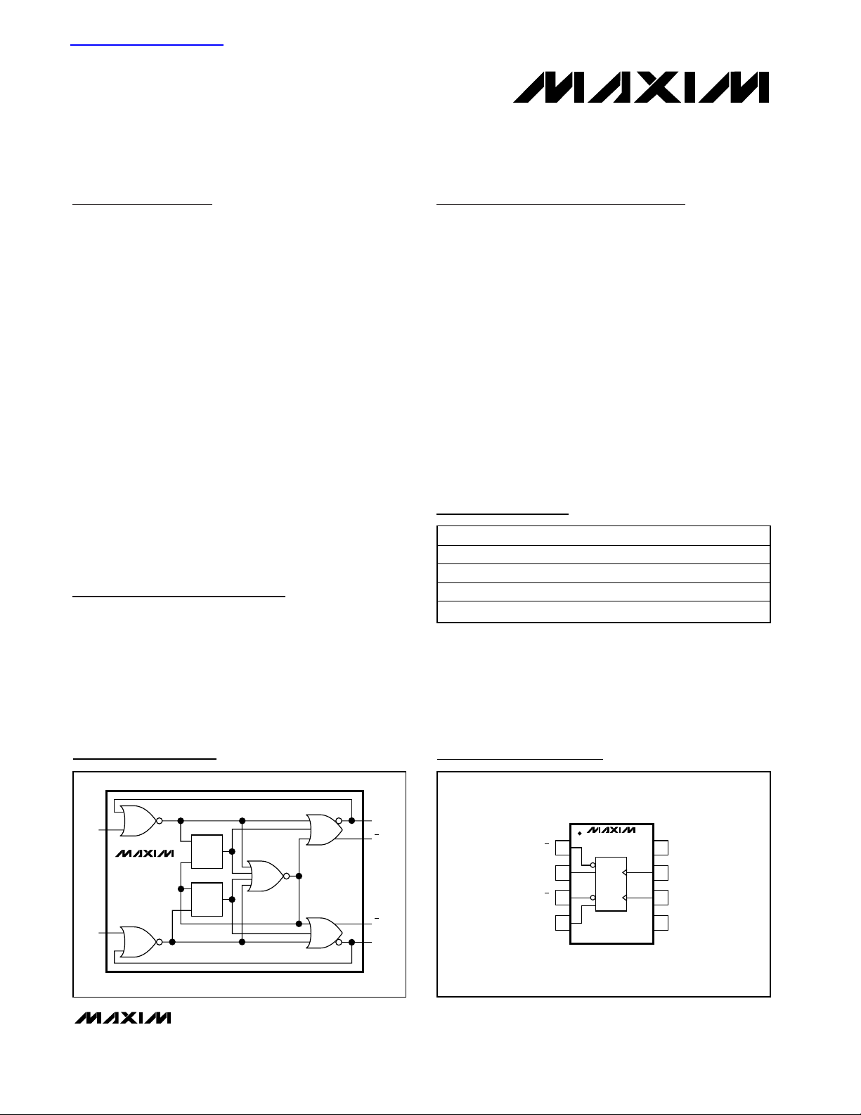
The MAX9382/MAX9383 are high-speed PECL/ECL
phase-frequency detectors designed for use in highbandwidth phase-locked loop (PLL) applications. The
devices compare a single-ended reference (R) and a
VCO (V) input and produce pulse streams on differential up (U) and down (D) outputs. When integrated, the
difference of the output pulse streams provides a control voltage proportional to input phase or frequency difference. Guaranteed minimum short pulse duration
completely eliminates minimum phase difference
requirements during the lock condition, maximizing
loop jitter performance.
The MAX9382/MAX9383 feature low propagation and
reset delay, making them ideal for high-frequency clock
synchronization use. The MAX9382 uses 100K logic
levels, has a supply voltage range of VCC- VEE= 4.2V
to 5.5V, and is pin compatible with Motorola’s
MCK12140. The MAX9383 uses 10H logic levels with a
supply voltage range of VCC- VEE= 4.75V to 5.5V and
is pin compatible with the MCH12140.
The MAX9382/MAX9383 are available in industry-standard 8-pin SO and space-saving 8-pin µMAX packages.
Applications
Precision Clock Distribution
Central Office
DSLAM
DLC
Base Station
ATE
Features
♦ Guaranteed Minimum Pulse Width Eliminates
Dead Band
♦ 450MHz Typical Bandwidth with up to ±π Phase
Detection
♦ 75kΩ Internal Input Pulldown Resistors
♦ 44mA Typical Supply Current
♦ ±2kV ESD Protection (Human Body Model)
♦ Pin Compatible with MCK12140 and MCH12140
♦ Available in 8-Pin µMAX and SO Packages
MAX9382/MAX9383
ECL/PECL Phase-Frequency Detectors
________________________________________________________________ Maxim Integrated Products 1
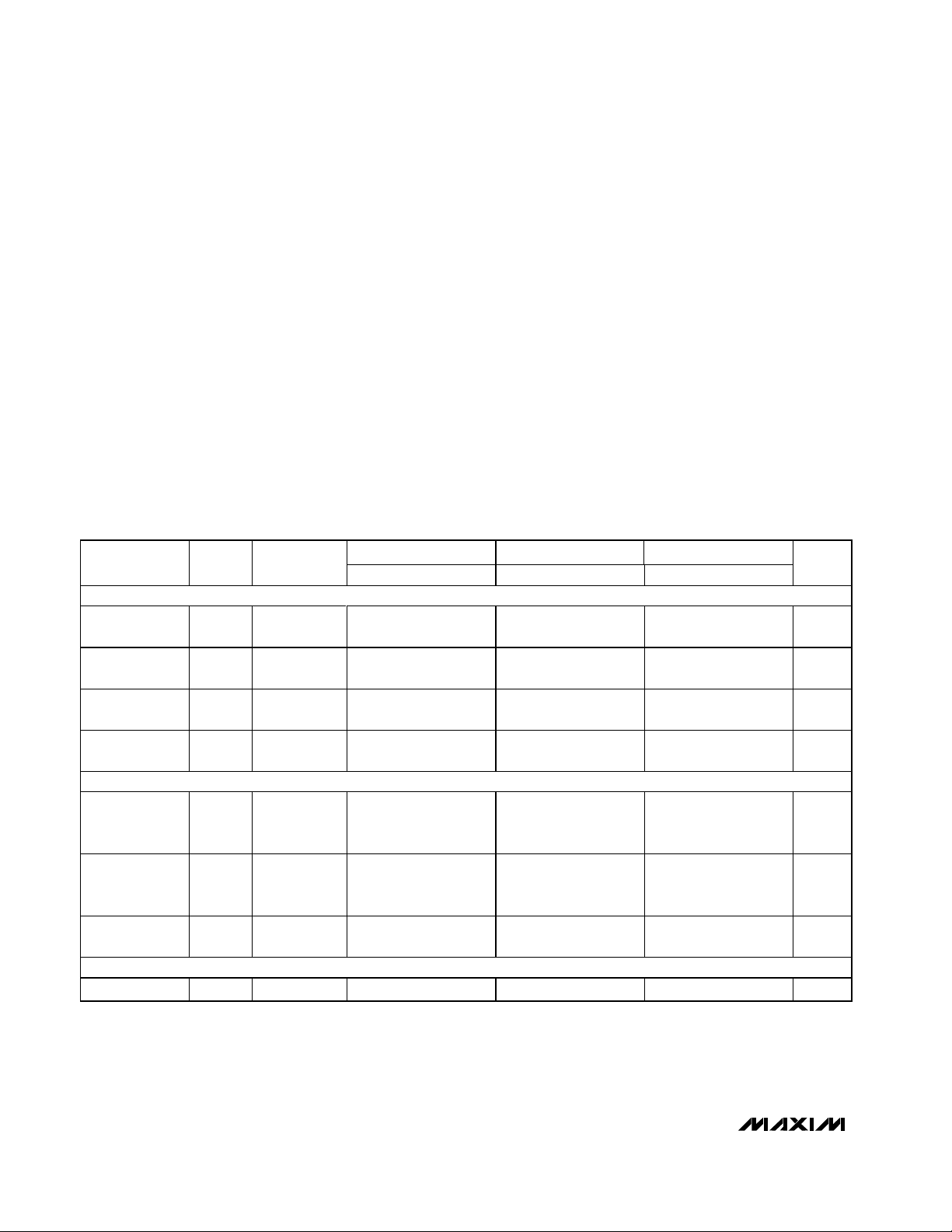
Pin Configuration
Ordering Information
19-2234; Rev 1; 11/02
*Future product—contact factory for availability.
For pricing, delivery, and ordering information, please contact Maxim/Dallas Direct! at
1-888-629-4642, or visit Maxim’s website at www.maxim-ic.com.
Functional Diagram
查询MAX9382供应商
PART TEMP RANGE PIN-PACKAGE
MAX9382EUA* -40°C to +85°C 8 µMAX
MAX9382ESA -40°C to +85°C 8 SO
MAX9383EUA* -40°C to +85°C 8 µMAX
MAX9383ESA -40°C to +85°C 8 SO
TOP VIEW
R
MAX9382
MAX9383
V
R
Q
S
S
Q
R
U
U
D
D
U
1
2
D
3
4
D
MAX9382
MAX9383
µMAX/SO
87V
6
5
CC
RU
V
V
EE
Page 2
MAX9382/MAX9383
ECL/PECL Phase-Frequency Detectors
2 _______________________________________________________________________________________
ABSOLUTE MAXIMUM RATINGS
MAX9382 DC ELECTRICAL CHARACTERISTICS
(VCC- VEE= 4.2V to 5.5V. Outputs loaded with 50Ω ±1% to VCC- 2V, unless otherwise noted. Typical values at VCC- VEE= 4.5V.)
(Notes 1, 2, 3)
Stresses beyond those listed under “Absolute Maximum Ratings” may cause permanent damage to the device. These are stress ratings only, and functional
operation of the device at these or any other conditions beyond those indicated in the operational sections of the specifications is not implied. Exposure to
absolute maximum rating conditions for extended periods may affect device reliability.
VCC- VEE............................................................................+6.0V
Inputs (R, V).................................................(V
CC
) to (VEE- 0.3V)
Continuous Output Current .................................................50mA
Surge Output Current........................................................100mA
Junction-to-Ambient Thermal Resistance in Still Air*
8-Pin µMAX ..............................................................+221°C/W
8-Pin SO ..................................................................+170°C/W
Junction-to-Ambient Thermal Resistance with*
500LFPM Airflow
8-Pin µMAX ..............................................................+155°C/W
8-Pin SO.....................................................................+99°C/W
Junction-to-Case Thermal Resistance
8-Pin µMAX ...............................................................+39°C/W
8-Pin SO....................................................................+40°C/W
Operating Temperature Range ...........................-40°C to +85°C
Junction Temperature......................................................+150°C
Storage Temperature Range .............................-65°C to +150°C
ESD Protection
Human Body Model (R, V, U, U, D, D)............................±2kV
Soldering Temperature (10s) .......................................... +300°C
*Ratings are for single-layer board.
PARAMETER
INPUTS (R, V)
Input High
Voltage
Input Low
Voltage
Input High
Current
Input Low
Current
OUTPUTS (U, U, D, D)
Single-Ended
Output High
Voltage
SYMBOL
V
IH
V
IL
I
IH
I
IL
V
OH
CONDITIONS
VIN = V
IHMAX
VIN = V
ILMIN
VIN = VIH or
V
IL
VCC -
1.165
VCC -
1.810
VCC -
1.085
-40°C
MIN TYP MAX MIN TYP MAX MIN TYP MAX
0.5 0.5 0.5 µA
VCC -
0.990
VCC -
1.165
VCC -
1.810
VCC -
1.035
+85°C
VCC -
0.940
VCC -
0.880
VCC -
1.475
VCC -
0.880
+25°C
VCC -
0.880
VCC -
1.475
VCC -
0.880
VCC -
1.165
VCC -
1.810
150 150 150 µA
VCC -
1.035
VCC -
0.960
VCC -
0.880
VCC -
1. 475
VCC -
0.880
UNITS
V
V
V
Single-Ended
Output Low
Voltage
Differential
Output Voltage
POWER SUPPLY
Supply Current I
V
VOH -
V
EE
VIN = VIH or
OL
V
IL
VIN = VIH or
V
OL
IL
(Note 4) 43 56 44 56 45 58 mA
VCC -
1.890
VCC -
1.810
585 820 585 810 585 800 mV
VCC -
1.555
VCC -
1.850
VCC -
1.770
VCC -
1.620
VCC -
1.810
VCC -
1.730
VCC -
1.600
V
Page 3
MAX9382/MAX9383
ECL/PECL Phase-Frequency Detectors
_______________________________________________________________________________________ 3
MAX9383 DC ELECTRICAL CHARACTERISTICS
(VCC- VEE= 4.75V to 5.5V. Outputs loaded with 50Ω ±1% to VCC- 2V, unless otherwise noted. Typical values at VCC- VEE= 5.2V.)
(Notes 1, 2, 3)
MAX9382/MAX9383 AC ELECTRICAL CHARACTERISTICS
(Over specified DC input parameters, f = 100MHz, outputs loaded with 50Ω ±1% to VCC- 2V, unless otherwise noted.) (Note 5)
PARAMETER SYMBOL CONDITIONS
INPUTS (R, V)
Input High
Voltage
Input Low
Voltage
Input High
Current
Input Low
Current
OUTPUTS (U, U, D, D)
Single-Ended
Output High
Voltage
Single-Ended
Output Low
Voltage
Differential
Output Voltage
POWER SUPPLY
Supply Current I
V
IH
V
IL
I
IH
I
IL
V
OH
V
OL
VOH -
V
OL
EE
VIN = V
IHMAX
VIN = V
ILMIN
VIN = VIH or
V
IL
VIN = VIH or
V
IL
VIN = VIH or
V
IL
(Note 4) 37 52 38 52 39 52 mA
VCC -
1.230
VCC -
1.950
0.5 0.5 0.5 µA
VCC -
1.115
VCC -
1.990
650 822 650 817 650 803 mV
-40°C +25°C +85°C
MIN TYP MAX MIN TYP MAX MIN TYP MAX
VCC -
1.010
VCC -
1.832
VCC -
0.890
VCC -
1.500
150 150 150 µA
VCC -
0.890
VCC -
1.650
VCC -
1.130
VCC -
1.950
VCC -
0.980
VCC -
1.950
VCC -
0.924
VCC -
1.740
VCC -
0.810
VCC -
1. 480
VCC -
0.810
VCC -
1.630
VCC -
1.060
VCC -
1.950
VCC -
0.945
VCC -
1.950
VCC -
0.900
VCC -
1.700
VCC -
0.720
VCC -
1.480
VCC -
0.720
VCC -
1.595
UNITS
V
V
V
V
PARAMETER SYMBOL CONDITIONS
R Input to U
Output Delay
V Input to D
Output Delay
R Input to D
Output Delay
V Input to U
Output Delay
Minimum Pulse
Duration
t
PRU
t
PVD
t
PRD
t
PVU
t
Pmin
Figure 1 575 650 750 590 660 780 635 720 830 ps
Figure 1 575 650 750 590 660 780 635 720 830 ps
Figure 1 945 1120 1320 960 1110 1360 1005 1150 1360 ps
Figure 1 945 1120 1320 960 1110 1360 1005 1150 1360 ps
Figure 1 370 470 370 450 370 430 ps
MIN TYP MAX MIN TYP MAX MIN TYP MAX
-40°C +25°C +85°C
UNITS
Page 4

MAX9382/MAX9383
ECL/PECL Phase-Frequency Detectors
4 _______________________________________________________________________________________
Note 1: Measurements are made with the device in thermal equilibrium.
Note 2: Current into a pin is defined as positive. Current out of a pin is defined as negative.
Note 3: DC parameters are production tested at +85°C. DC limits are guaranteed by design and characterization over the full oper-
ating temperature range.
Note 4: All pins open except V
CC
and VEE.
Note 5: Guaranteed by design and characterization. Limits are set to ±6 sigma.
Note 6: Phase offset is defined as the difference in propagation delay timing between the two input paths. It is measured between
the U and D outputs at the differential crosspoint with a rising edge simultaneously applied at the R and V inputs.
Note 7: Device jitter added to the input signal.
MAX9382/MAX9383 AC ELECTRICAL CHARACTERISTICS (continued)
(Over specified DC input parameters, f = 100MHz, outputs loaded with 50Ω ±1% to VCC- 2V, unless otherwise noted.) (Note 5)
PARAMETER SYMBOL CONDITIONS
MIN TYP MAX MIN TYP MAX MIN TYP MAX
-40°C +25°C +85°C
UNITS
RJ
, t
F
±π usable
phase
difference
range
= 200MHz,
V
IN
50% duty
cycle (Note 6)
VIN = 400MHz,
50% duty
cycle (Note 7)
20% to 80%,
Figure 2
400 450 400 450 400 450
30 70 28 60 28 60
0.2 1.0 0.2 1.0 0.2 1.0
80 160 100 180 110 190 ps
Maximum
Operating
Frequency
Phase Offset
Added Random
Jitter
Output Rise/ Fall
Time
f
t
R
MAX
t
MHz
ps
ps
(RMS)
Page 5

MAX9382/MAX9383
ECL/PECL Phase-Frequency Detectors
_______________________________________________________________________________________ 5
Typical Operating Characteristics
(VCC- VEE= +4.5V (MAX9382) or VCC- VEE= +5.2V (MAX9383), VIH= VCC- 1.00V, VIL= VCC- 1.60V, fR= fV= 100MHz, outputs
loaded with 50Ω to V
CC
- 2V, TA= +25°C, unless otherwise noted.)
SUPPLY CURRENT vs. TEMPERATURE
45.0
42.5
40.0
37.5
35.0
SUPPLY CURRENT (mA)
32.5
30.0
-40 35-15 10 60
550
525
500
475
150
MAX9382
MAX9383
TEMPERATURE (°C)
MAX9382/83 toc01
85
125
100
TRANSITION TIME (ps)
75
50
OUTPUT SHORT-PULSE DURATION
vs. TEMPERATURE
MAX9382
TRANSITION TIME vs. TEMPERATURE
MAX9382
RISE TIME
FALL TIME
-40 10-15 35 60 85
TEMPERATURE (°C)
750
MAX9382/83 toc04
725
700
675
200
MAX9382/83 toc02
175
150
TRANSITION TIME (ps)
125
100
PROPAGATION DELAY
vs. TEMPERATURE
t
OR t
PRU
PVD
MAX9383
TRANSITION TIME vs. TEMPERATURE
MAX9383
RISE TIME
FALL TIME
-40 10-15 35 60 80
TEMPERATURE (°C)
MAX9382/83 toc05
MAX9382/83 toc03
450
425
OUTPUT SHORT-PULSE DURATION (ps)
400
-40 10-15 35 60 80
TEMPERATURE (°C)
DIFFERENTIAL OUTPUT VOLTAGE
vs. FREQUENCY
830
820
MAX9383
810
MAX9382
800
790
780
DIFFERENTIAL OUTPUT VOLTAGE (V)
770
0 2000
FREQUENCY (MHz)
MAX9383
15001000500
MAX9382/83 toc06
650
PROPAGATION DELAY (ps)
MAX9382
625
600
-15
-40 35
10 60
TEMPERATURE (°C)
OUTPUT PHASE ERROR
vs. INPUT PHASE DIFFERENCE
50
40
30
20
OUTPUT PHASE ERROR (ps)
10
0
-4 0-2 2 4
INPUT PHASE DIFFERENCE (ns)
85
MAX9382/83 toc07
Page 6

MAX9382/MAX9383
Detailed Description
The MAX9382/MAX9383 are high-speed phase or frequency detectors. The MAX9382 is compatible with 100K
logic and has a power-supply range of VCC- V
EE
= 4.2V
to 5.5V. The MAX9383 is compatible with 10H logic with a
power-supply range of VCC- VEE= 4.75V to 5.5V. Both
devices are specified to function from -40°C to +85°C.
Each device is symmetrical; the R and V input functions
may be swapped, together with the U and D output
functions, and the inputs and outputs relabeled.
Because of this device symmetry, a necessary condition for correct phase measurement operation is that
the U and D outputs must both be high (state 0 condition) when the rising edge of the leading input is
received. This condition is automatically generated
when the two inputs are at different frequencies.
Phase Detection
The MAX9382/MAX9383 are intended for use in highbandwidth PLL applications. These devices compare a
single-ended VCO input (V) to a single-ended reference input (R) to determine the phase or frequency
relationship between V and R. The device differential
outputs U, U and D, D provide pulse trains with duty
cycle proportional to the phase or frequency difference
between R and V. These outputs are the up and down
signals required to control the system VCO. Figure 1
shows typical waveforms when V leads R and V lags R.
Subtracting and integrating these two outputs provide
the necessary VCO control signal. Figure 3 shows the
device transfer function obtained. The detector can
detect phase differences up to ±2π. The application
frequency and the characteristics of the device internal
reset circuits determine the usable input phase difference range.
Frequency Detection
Figure 4 is the state diagram for the MAX9382/
MAX9383. With the two inputs at the same frequency,
and input R leading input V, the device toggles
between states 0 and 2. Similarly, if input R lags input
V, the device toggles between states 0 and 1. With the
two inputs at different frequencies, the output becomes
a function of the frequency difference. The normalized
ideal transfer function is given by:
and
Output Pulses
When inputs R and V are at the same phase and frequency, outputs U, U and D, D produce a stream of
minimum duration pulses that occur at the rising edges
of the input waveforms. This is the lock condition. If
either input starts to lead the other in phase, the width
of pulses on the corresponding output (U for R input, D
for V input) increases in proportion to the phase difference. In a PLL implementation, these outputs direct the
ECL/PECL Phase-Frequency Detectors
6 _______________________________________________________________________________________
Pin Description
PIN NAME FUNCTION
1 U
2U
3 D
4D
5VEENegative Supply
6 V Single-Ended VCO Input
7 R Single-Ended Reference Input
8V
CC
Inverting Up Output. Pulse stream is generated at this pin when f
Terminate with 50Ω resistor to V
Noninverting Up Output. Pulse stream is generated at this pin when f
Terminate with 50Ω resistor to V
Inverting Down Output. Pulse stream is generated at this pin when f
Terminate with 50Ω resistor to V
Noninverting Down Output. Pulse stream is generated at this pin when f
Terminate with 50Ω resistor to V
Positive Supply. Bypass from VCC to VEE with 0.1µF and 0.01µF ceramic capacitors. Place the
capacitors as close to the device as possible with the smaller value capacitor closest to the device.
- 2V or equivalent.
CC
- 2V or equivalent.
CC
- 2V or equivalent.
CC
- 2V or equivalent.
CC
> fV or V lags R in phase.
R
> fV or V lags R in phase.
R
> fR or R lags V in phase.
V
> fR or R lags V in phase.
V
V
OUT AVE
V
OUT AVE
=>12-
=>12-
f
R
f
V
f
V
for f f
f
R
for f f
VR_
RV_
Page 7

system VCO to increase or decrease frequency to
maintain the lock condition.
The minimum output pulse duration is an important
parameter for the design of the signal processing functions, which follow the phase detector. When controlling
a charge-pump integrator, a detector can produce a
dead-zone characteristic at the lock condition if the
minimum pulse width is too short. MAX9382/MAX9383
eliminate this dead-zone characteristic, and the resulting phase offset at lock, by providing a well-defined
minimum output pulse width.
Applications Information
The MAX9382/MAX9383 input and output levels are
defined to be relative to the positive supply voltage. In
ECL systems, the positive supply voltage is conventionally chosen to be system ground. This arrangement
produces the best noise immunity, since ground is normally a system-wide reference voltage. Operate the
devices with V
CC
connected to ground and VEEcon-
nected to a negative supply for ECL systems. With
PECL systems, connect V
CC
to a positive supply and
VEEto ground.
Power-Supply Bypassing
Adequate power-supply bypassing is necessary to
maximize the performance and noise immunity of ECL
devices. This is particularly true of a PECL system
where the power-supply voltage is used as a reference.
Bypass VCCto VEEwith high-frequency surface-mount
ceramic 0.1µF and 0.01µF capacitors in parallel and as
close to the device as possible, with the 0.01µF capaci-
MAX9382/MAX9383
ECL/PECL Phase-Frequency Detectors
_______________________________________________________________________________________ 7
Figure 1. Typical Waveforms when fR= f
V
Figure 2. Output Transition Times
R
V
U
U
D
D
t
PRU
a) INPUT AND OUTPUT WAVEFORMS FOR V LEADING R
R
V
U
U
D
D
t
PVD
b) INPUT AND OUTPUT WAVEFORMS FOR V LAGGING R
t
PVU
t
PRD
t
t
Pmin
Pmin
t
80%
20%
F
U - U
OR
D - D
20%
80%
t
R
Page 8

MAX9382/MAX9383
tor closest to the device pins. Use multiple parallel vias
for ground plane connection to minimize inductance.
Circuit Board Traces
Input and output trace characteristics affect the performance of ECL/PECL devices. Connect each of the
detector’s inputs and outputs to a 50Ω characteristic
impedance trace. Avoid impedance discontinuities,
maintain the distance between differential traces, avoid
sharp corners, and keep the electrical length of the differential traces matched. This maximizes commonmode noise rejection and reduces signal skew. Trace
vias cause impedance discontinuities, so keep the
number of vias in the 50Ω traces to a minimum. Reduce
reflections by maintaining the 50Ω characteristic
impedance through connectors and across cables.
Output Termination
Terminate outputs through 50Ω to VCC- 2V or use an
equivalent Thevenin termination. When a single-ended
signal is taken from a differential output, terminate both
outputs. For example, if the U output of the MAX9382 or
MAX9383 is connected to a single-ended input, terminate both the U and U outputs.
Chip Information
TRANSISTOR COUNT: 706
PROCESS: Bipolar
ECL/PECL Phase-Frequency Detectors
8 _______________________________________________________________________________________
Figure 3. Average Output Voltage vs. Phase Difference
Figure 4. MAX9382/MAX9383 State Diagram
AVG
AVG
AVG
(U - D)
> f
f
V
R
OR
V LEADS R
(U)
(D)
0
π 2π-π-2π
< f
f
V
OR
V LAGS R
R
3π 4π-3π-4π
V
OH
V
OL
V
OH
V
OL
VOH - V
0
V
- V
OL
OL
OH
VR
STATE 0STATE 2
R
U = 0
D = 1
V
VCO
UP
U = 1
D = 1
VCO
DOWN
R
STATE 1
U = 1
D = 0
V
Page 9

MAX9382/MAX9383
ECL/PECL Phase-Frequency Detectors
_______________________________________________________________________________________ 9
Package Information
(The package drawing(s) in this data sheet may not reflect the most current specifications. For the latest package outline information,
go to www.maxim-ic.com/packages.)
0.6±0.1
0.6±0.1
8
b
E H
A1
A
ÿ 0.50±0.1
1
D
TOP VIEW
A2
e
FRONT VIEW
4X S
BOTTOM VIEW
c
L
SIDE VIEW
8
1
DIM
A
A1
A2
b
c
D
e
E
H
L
α
S
INCHES
MIN
-
0.002
0.030
0.010
0.005
0.116
0.0256 BSC
0.116
0.188
0.016
0∞
0.0207 BSC
MAX
0.043
0.006
0.037
0.014
0.007
0.120
0.120
0.198
0.026
6∞
MILLIMETERS
0.05 0.15
0.25 0.36
0.13 0.18
2.95 3.05
2.95 3.05
4.78
0.41
MIN
- 1.10
0.65 BSC
0.5250 BSC
MAX
0.950.75
5.03
0.66
8LUMAXD.EPS
6∞0∞
α
PROPRIETARY INFORMATION
TITLE:
PACKAGE OUTLINE, 8L uMAX/uSOP
REV.DOCUMENT CONTROL NO.APPROVAL
21-0036
1
J
1
Page 10

MAX9382/MAX9383
ECL/PECL Phase-Frequency Detectors
Maxim cannot assume responsibility for use of any circuitry other than circuitry entirely embodied in a Maxim product. No circuit patent licenses are
implied. Maxim reserves the right to change the circuitry and specifications without notice at any time.
10 ____________________Maxim Integrated Products, 120 San Gabriel Drive, Sunnyvale, CA 94086 408-737-7600
© 2002 Maxim Integrated Products Printed USA is a registered trademark of Maxim Integrated Products.
Package Information (continued)
(The package drawing(s) in this data sheet may not reflect the most current specifications. For the latest package outline information,
go to www.maxim-ic.com/packages.)
N
HE
1
TOP VIEW
D
A
e
FRONT VIEW
B
A1
INCHES
DIM
MIN
0.053A
0.004
A1
0.014
B
0.007
C
e 0.050 BSC 1.27 BSC
0.150
E
H 0.2440.228 5.80 6.20
0.016L
VARIATIONS:
INCHES
MINDIM
D
0.189 0.197 AA5.004.80 8
0.337 0.344 AB8.758.55 14
D
C
L
0∞-8∞
MAX
0.069
0.010
0.019
0.010
0.157
0.050
MAX
0.3940.386D
MILLIMETERS
MAX
MIN
1.35
1.75
0.10
0.25
0.35
0.49
0.19
0.25
3.80 4.00
0.40 1.27
MILLIMETERS
MAX
MIN
9.80 10.00
N MS012
16
AC
SOICN .EPS
SIDE VIEW
PROPRIETARY INFORMATION
TITLE:
PACKAGE OUTLINE, .150" SOIC
REV.DOCUMENT CONTROL NO.APPROVAL
21-0041
1
B
1
 Loading...