

Page 1
General Description
The MAX9380 is a high-speed, low-jitter 2:1 multiplexer
for clock and data distribution applications. The device
selects one of the two single-ended inputs and converts it to a differential output.
The MAX9380 features low part-to-part skew of 33ps
and propagation delay of 263ps.
The MAX9380 operates from a +3.0V to +3.8V supply for
LVPECL applications or from a -3.0V to -3.8V supply for
LVECL applications. The input is selected by a single select
input. The select and data inputs feature internal pulldown
resistors that ensure a low default state if left open.
These devices are specified for operation from -40°C to
+85°C, and are available in space-saving 8-pin µMAX
and SO packages.
Applications
Precision Clock Distribution
DSLAM
DLC
Base Station
ATE
Features
♦ >300mV Differential Output at 3.5GHz
♦ Low 20mA Supply Current
♦ 33ps (typ) Part-to-Part Skew
♦ 263ps (typ) Propagation Delay
♦ <0.2ps
RMS
Added Random Jitter
♦ High-Speed Select Input
♦ Output Low with Open Inputs
♦ Pin Compatible with MC10EP58
MAX9380
Single-Ended-to-Differential
LVECL/LVPECL 2:1 Multiplexer
________________________________________________________________ Maxim Integrated Products 1
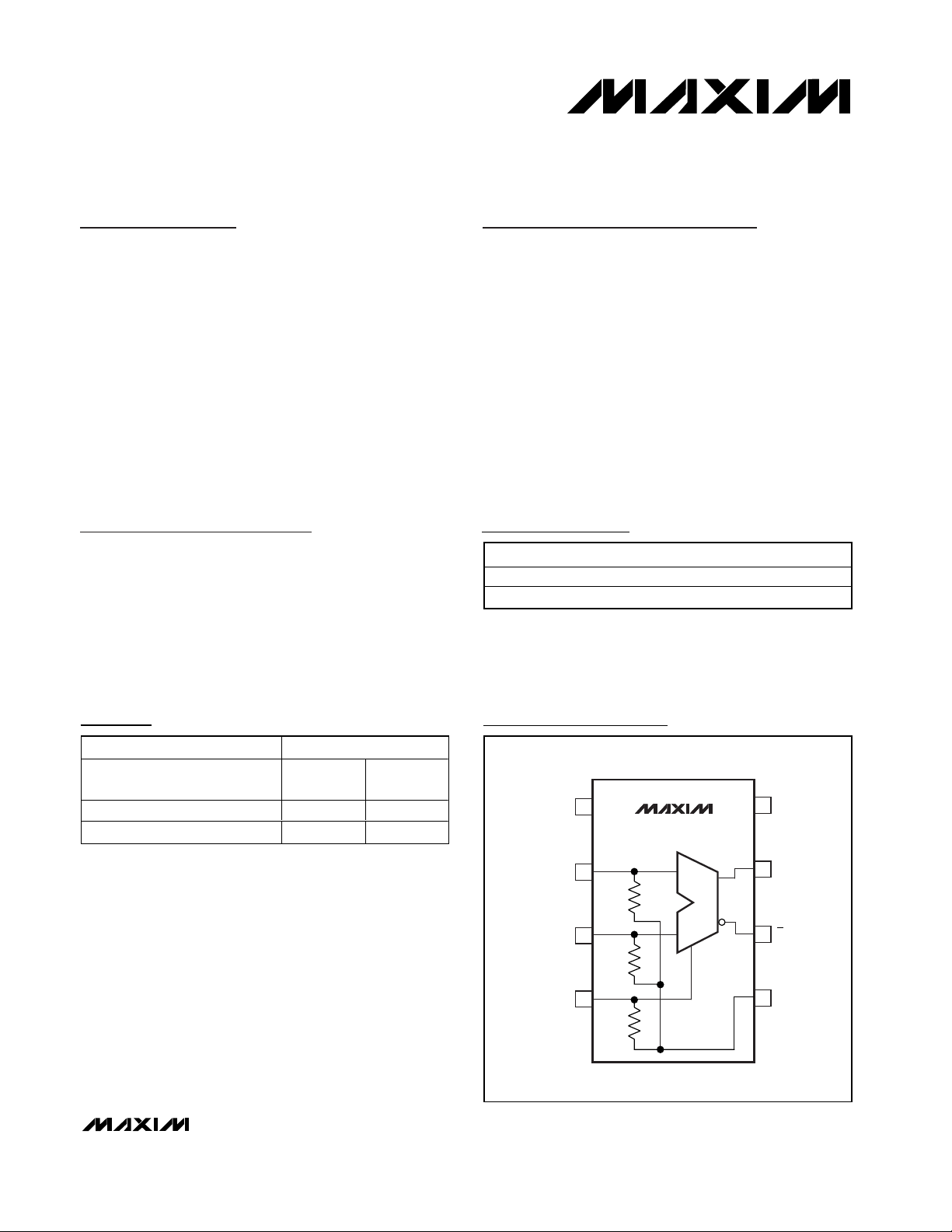
Pin Configuration
INPUTS OUTPUTS
Da (SEL = high) or
Db (SEL = low)
Q Q
High H L
Low or open L H
PART
PIN-PACKAGE
MAX9380EUA*
8 µMAX
MAX9380ESA
8 SO-EP**
Input/Output Function Table
19-2236; Rev 0; 10/01
For pricing, delivery, and ordering information, please contact Maxim/Dallas Direct! at
1-888-629-4642, or visit Maxim’s website at www.maxim-ic.com.
Ordering Information
*Future product—contact factory for availability.
**EP = Exposed paddle.
TEMP. RANGE
-40°C to +85°C
-40°C to +85°C
TOP VIEW
NC
Db
SEL
1
MAX9380
2Da
75kΩ
3
75kΩ
4
75kΩ
1
0
µMAX/SO
87V
6
5
CC
Q
Q
V
EE
Page 2
MAX9380
Single-Ended-to-Differential
LVECL/LVPECL 2:1 Multiplexer
2 _______________________________________________________________________________________
ABSOLUTE MAXIMUM RATINGS
DC ELECTRICAL CHARACTERISTICS
(VCC- VEE= +3.0V to +3.8V, outputs terminated with 50Ω to VCC- 2.0V, unless otherwise noted.) (Notes 1, 2, 3)
Stresses beyond those listed under “Absolute Maximum Ratings” may cause permanent damage to the device. These are stress ratings only, and functional
operation of the device at these or any other conditions beyond those indicated in the operational sections of the specifications is not implied. Exposure to
absolute maximum rating conditions for extended periods may affect device reliability.
VCC- VEE...............................................................-0.3V to +4.1V
Inputs (Da, Db, SEL).............................V
EE
- 0.3V to VCC+ 0.3V
Output Current (Continuous)...............................................50mA
Output Current (Surge) .....................................................100mA
Junction-to-Ambient Thermal Resistance in Still Air
8-Pin µMAX ..............................................................+221°C/W
8-Pin SO* .................................................................+170°C/W
Junction-to-Ambient Thermal Resistance with
500LFPM Airflow
8-Pin µMAX ..............................................................+155°C/W
8-Pin SO* ...................................................................+99°C/W
Junction-to-Case Thermal Resistance
8-Pin µMAX ................................................................+39°C/W
8-Pin SO.....................................................................+40°C/W
Operating Temperature Range ...........................-40°C to +85°C
Junction Temperature......................................................+150°C
Storage Temperature Range .............................-65°C to +150°C
ESD Protection
Human Body Model (Inputs and Outputs) .........................2kV
Soldering Temperature (10s) ...........................................+300°C
* Rating is for exposed paddle not connected.
PARAMETER SYMBOL CONDITIONS
INPUTS (Da, Db, SEL)
Input High Voltage V
Input Low Voltage V
IH
IL
MIN TYP MAX MIN TYP MAX MIN TYP MAX
VCC -
1.210
VCC -
1.935
-40°C +25°C +85°C
VCC -
0.885
VCC -
1.610
VCC -
1.145
VCC -
1.870
VCC -
0.820
VCC -
1.545
VCC -
1.085
VCC -
1.81
VCC -
0.760
VCC -
1.485
UNITS
V
V
Input High Current I
Input Low Current I
OUTPUTS (Q, Q)
Single-Ended
Output High
Voltage
Single-Ended
Output Low
Voltage
Differential Output
Voltage
POWER SUPPLY
Supply Current I
VOH -
VIN = V
IH
IL
V
OH
V
OL
V
OL
EE
IH(MAX)
VIN = V
IL(MIN)
Figure 1
Figure 1
Figure 1 550 748 550 741 550 734 mV
(Note 4) 18 26 20 26 22 30 mA
0.5 0.5 0.5 µA
V
-
VCC -
CC
1.135
0.979
V
-
VCC -
CC
1.935
1.721
150 150 150 µA
VCC -
VCC -
VCC -
VCC -
VCC -
VCC -
VCC -
0.885
VCC -
1.685
1.07
VCC -
1.87
0.959
VCC -
1.698
0.82
VCC -
1.62
1.01
VCC -
1.81
0.947
VCC -
1.681
0.76
VCC -
1.56
V
V
Page 3
MAX9380
Single-Ended-to-Differential
LVECL/LVPECL 2:1 Multiplexer
_______________________________________________________________________________________ 3
AC ELECTRICAL CHARACTERISTICS
(VCC- VEE= +3.0V to +3.8V, outputs loaded with 50Ω to VCC- 2V, VIH= VCC- 1.11V, VIL= VCC- 1.53V, input frequency = 2.0GHz,
input transition time = 125ps (20% to 80%). Typical values are at V
CC
- VEE= +3.3V, unless otherwise noted.) (Notes 1, 5)
Note 1: Measurements are made with the device in thermal equilibrium.
Note 2: Current into a pin is defined as positive. Current out of a pin is defined as negative.
Note 3: DC parameters are production tested at +25°C. DC limits are guaranteed by design and characterization over the full oper-
ating temperature range.
Note 4: All pins are open except V
CC
and VEE.
Note 5: Guaranteed by design and characterization. Limits are set to ±6 sigma.
Note 6: Measured between outputs of different parts at the signal crossing points under identical conditions for a same-edge transition.
Note 7: Device jitter added to the input signal.
PARAMETER SYMBOL CONDITIONS
Data Input-to-Output
Delay
Select Input-toOutput Delay
Part-to-Part Skew t
Added Random
Jitter (Note 7)
Added Deterministic
Jitter (Note 7)
Switching Frequency f
Output Rise/Fall
Time (20% to 80%)
t
PLH1
t
PHL1
t
PLH2
t
PHL2
SKPP
t
t
MAX
t
R
,
Figure 1 176 258 298 192 263 316 222 277 385 ps
,
Figure 2 210 304 329 219 308 360 247 318 392 ps
,
Data input to
output (Note 6)
fIN = 3.2GHz,
RJ
clock pattern
2.0Gbps, 223 - 1
PRBS
DJ
3.2Gbps, 223 - 1
PRBS
VOH - VOL ≥
300mV
1
V
550mV
Figure 1 50 96 50 96 50 98 ps
, t
Figure
F
OH
- VOL ≥
MIN TYP MAX MIN TYP MAX MIN TYP MAX
3.0 3.5 3.0 3.5 3.0 3.5
2.0 2.0 2.0
-40°C +25°C +85°C
27 122 33 124 14 163 ps
1.2 0.2 1.2 1.2
51 36 51 51
77 48 77 77
UNITS
ps
(RMS)
ps
(p-p)
GHz
Page 4

MAX9380
Single-Ended-to-Differential
LVECL/LVPECL 2:1 Multiplexer
4 _______________________________________________________________________________________
Typical Operating Characteristics
(VCC- VEE= +3.3V, VIH= VCC- 1.165V, VIL= VCC- 1.475V, outputs loaded with 50Ω to VCC- 2.0V, input frequency = 1GHz, input
transition time = 125ps (20% to 80%), unless otherwise noted.)
30
25
20
15
10
-40 10-15 35 60 85
SUPPLY CURRENT (IEE)
vs. TEMPERATURE
MAX9380 toc01
TEMPERATURE (°C)
SUPPLY CURRENT (mA)
0.20
0.40
0.60
0.80
1.00
OUTPUT AMPLITUDE (VOH - VOL)
vs. FREQUENCY
MAX9380 toc02
FREQUENCY (MHz)
OUTPUT AMPLITUDE (V)
0 1500 2000500 1000 2500 3000 3500
OUTPUT RISE/FALL TIME
vs. TEMPERATURE
MAX9380 toc03
TEMPERATURE (°C)
OUTPUT RISE/FALL TIME (ps)
603510-15
75
80
85
90
95
100
70
-40 85
t
F
t
R
180
220
200
260
240
300
280
320
-40 10-15 35 60 85
PROPAGATION DELAY
vs. TEMPERATURE
MAX9380 toc04
TEMPERATURE (°C)
PROPAGATION DELAY (ps)
t
PHL1
t
PLH1
Page 5

MAX9380
Single-Ended-to-Differential
LVECL/LVPECL 2:1 Multiplexer
_______________________________________________________________________________________ 5
Pin Description
Figure 1. Data Input-to-Output Propagation Delay and Transition Timing Diagram
PIN NAME FUNCTION
1 NC No Connection. Not internally connected.
2 Da Single-Ended LVECL/LVPECL Data Input. Da is low default through internal 75kΩ pulldown resistor.
3 Db Single-Ended LVECL/LVPECL Data Input. Db is low default through internal 75kΩ pulldown resistor.
4 SEL
Single-Ended Control Input. SEL is low default through an internal 75kΩ pulldown resistor selecting Db.
Setting SEL to high selects Da.
5VEENegative Supply Voltage
6 Q Differential LVECL/LVPECL Output. Open Emitter. Q is default high when inputs are open.
7 Q Differential LVECL/LVPECL Output. Open Emitter. Q is default low when inputs are open.
8V
E xp osed
P ad d l e
CC
EP Exposed paddle (MAX9380ESA-EP only). Connect to V
Da WHEN SEL = HIGH
Db WHEN SEL = LOW
Positive Supply Voltage. Bypass VCC to VEE with 0.1µF and 0.01µF capacitors as close to the device as
possible, with the smaller capacitor closest to the IC.
internally. See package dimension.
EE
50%50%
OR
t
PLH1
t
PHL1
V
IH
V
IL
Q
SINGLE-ENDED WAVEFORMS
Q
DIFFERENTIAL WAVEFORM
Q - Q
20%
80% 80%
t
R
V
OH - VOL
V
OH - VOL
V
OH - VOL
0 (DIFFERENTIAL)
t
F
20%
V
OH
V
OL
Page 6

MAX9380
Single-Ended-to-Differential
LVECL/LVPECL 2:1 Multiplexer
6 _______________________________________________________________________________________
Detailed Description
The MAX9380 is a high-speed, low-jitter 2:1 multiplexer
designed for clock and data distribution. The device
selects one of the two single-ended inputs.
The multiplexer function is controlled by the singleended SEL input. A high level on the SEL input selects
the single-ended data input Da. Similarly, a low level on
the SEL input selects the single-ended data input Db.
The selected input is converted to a differential signal
at the Q and Q outputs.
The inputs Da, Db, and SEL have a 75kΩ pulldown to
VEE. This ensures that an open input has a low state. All
inputs can be driven from a single-ended LVECL/
LVPECL signal or to VEEand VCC.
Applications Information
LVECL/LVPECL
In LVECL systems, the positive supply voltage is conventionally chosen to be system ground. This arrangement produces the best noise immunity since ground is
normally a system-wide reference voltage. Operate the
MAX9380 with V
CC
= 0 (ground) and VEE= -3.3V for an
LVECL system.
The MAX9380 operates in LVPECL systems by connecting VEEto ground and VCCto a positive supply
voltage. Connect V
CC
= +3.3V and VEE= 0 for an
LVPECL system.
Power-Supply Bypassing
Adequate power-supply bypassing is necessary to
maximize the performance and noise immunity. This is
particularly true of use in an LVPECL system where the
power-supply voltage is used as a reference. Bypass
VCCto VEEwith high-frequency surface-mount ceramic
0.1µF and 0.01µF capacitors in parallel as close to the
device as possible, with the 0.01µF capacitor closest to
the device pins. Use multiple parallel vias for ground
plane connection to minimize inductance.
Circuit Board Traces
Input and output trace characteristics affect the performance of ECL devices. Connect each of the MAX9380
inputs and outputs to a 50Ω characteristic impedance
trace. Avoid discontinuities in differential impedance
and maximize common-mode noise immunity by maintaining the distance between differential traces and
avoid sharp corners. Minimize the number of vias to
prevent impedance discontinuities. Reduce reflections
by maintaining the 50Ω characteristic impedance
through connectors and across cables. Minimize skew
by matching the electrical length of the traces.
Output Termination
Terminate outputs through 50Ω to VCC- 2V or use an
equivalent Thevenin termination. When a single-ended
signal is taken from a differential output, terminate both
outputs. For example, if the Q output of the MAX9380 is
connected to a single-ended input, terminate both the
Q and Q outputs.
Figure 2. Select Input-to-Output Propagation Delay and Transition Timing Diagram
V
IH
Da = HIGH
Db = LOW
SEL
Q
SINGLE-ENDED WAVEFORMS
Q
t
PLH2
t
PHL2
50%50%
V
IL
V
OH
V
OL
Page 7

Package Information
Chip Information
TRANSISTOR COUNT: 242
PROCESS: Bipolar
MAX9380
Single-Ended-to-Differential
LVECL/LVPECL 2:1 Multiplexer
_______________________________________________________________________________________ 7
8LUMAXD.EPS
Page 8

MAX9380
Single-Ended-to-Differential
LVECL/LVPECL 2:1 Multiplexer
Maxim cannot assume responsibility for use of any circuitry other than circuitry entirely embodied in a Maxim product. No circuit patent licenses are
implied. Maxim reserves the right to change the circuitry and specifications without notice at any time.
8 _____________________Maxim Integrated Products, 120 San Gabriel Drive, Sunnyvale, CA 94086 408-737-7600
© 2001 Maxim Integrated Products Printed USA is a registered trademark of Maxim Integrated Products.
Package Information (continued)
8L, SOIC EXP. PAD.EPS
 Loading...