

General Description
The MAX9377/MAX9378 are fully differential, highspeed, low-jitter anything-to-LVPECL and anything-toLVDS translators, respectively, with a selectable
divide-by-four function. Low propagation delay and
high speed make them ideal for various high-speed
network routing and backplane applications at speeds
up to 2GHz in nondivide mode.
The MAX9377/MAX9378 accept any differential input
signal within the supply rails and with minimum amplitude of 100mV. Inputs are fully compatible with the
LVDS, LVPECL, HSTL, and CML differential signaling
standards. The MAX9377 outputs are LVPECL and
have sufficient current to drive 50Ω transmission lines.
The MAX9378 outputs are LVDS and conform to the
ANSI EIA/TIA-644 LVDS standard.
The MAX9377/MAX9378 are available in 8-pin µMAX
packages and operate from a single +3.3V supply over
the -40°C to +85°C temperature range.
Applications
Backplane Logic Standard Translation
LAN
WAN
DSLAM
DLC
Features
♦ Guaranteed 2GHz Switching Frequency
♦ Accept LVDS/LVPECL/Anything Inputs
♦ Pin-Selectable Divide-by-Four Function
♦ 421ps (typ) Propagation Delays (MAX9377)
♦ 30ps (max) Pulse Skew
♦ 2ps
RMS
(max) Random Jitter
♦ Minimum 100mV Differential Input to Guarantee
AC Specifications
♦ Temperature-Compensated LVPECL Output
♦ +3.0V to +3.6V Power-Supply Operating Range
♦ ESD Protection: >2kV Human Body Model (HBM)
MAX9377/MAX9378
Anything-to-LVPECL/LVDS Translators
with Pin-Selectable Divide-by-Four
________________________________________________________________ Maxim Integrated Products 1
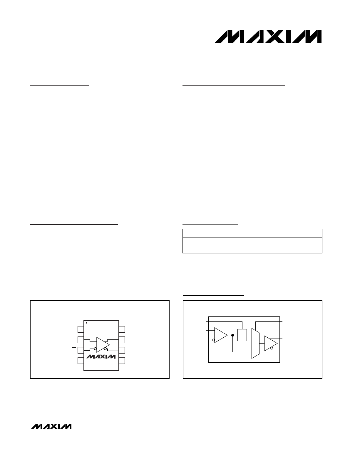
Pin Configuration
Ordering Information
19-2846; Rev 1; 7/03
For pricing, delivery, and ordering information, please contact Maxim/Dallas Direct! at
1-888-629-4642, or visit Maxim’s website at www.maxim-ic.com.
Functional Diagram
MAX9377EUA -40°C to +85°C 8 µMAX
MAX9378EUA -40°C to +85°C 8 µMAX
PART TEMP RANGE PIN-PACKAGE
TOP VIEW
RST
1
SEL
2
3
IN
4
MAX9377
MAX9378
87V
6
5
OUTIN
OUT
RSTGND
CC
LVDS/ANY
SEL
÷ 4
LVPECL (MAX9377)
OR
LVDS (MAX9378)
MAX9377/MAX9378
Anything-to-LVPECL/LVDS Translators
with Pin-Selectable Divide-by-Four
2 _______________________________________________________________________________________
ABSOLUTE MAXIMUM RATINGS
Stresses beyond those listed under “Absolute Maximum Ratings” may cause permanent damage to the device. These are stress ratings only, and functional
operation of the device at these or any other conditions beyond those indicated in the operational sections of the specifications is not implied. Exposure to
absolute maximum rating conditions for extended periods may affect device reliability.
VCCto GND...........................................................-0.3V to +4.1V
Inputs (IN, IN, RST, SEL)............................-0.3V to (V
CC
+ 0.3V)
IN to IN................................................................................±3.0V
Short-Circuit Duration (MAX9378 OUT, OUT) ............Continuous
Continuous Output Current .................................................50mA
Surge Output Current .......................................................100mA
Continuous Power Dissipation (T
A
= +70°C)
8-µMAX (derate 5.9mW/°C above +70°C) ...............470.6mW
θ
JA
in Still Air...........................................................+170°C/W
Junction Temperature......................................................+150°C
Storage Temperature Range .............................-65°C to +150°C
ESD Protection
Human Body Model (IN, IN, OUT, OUT) ..............................≥2kV
Soldering Temperature (10s) ...........................................+300°C
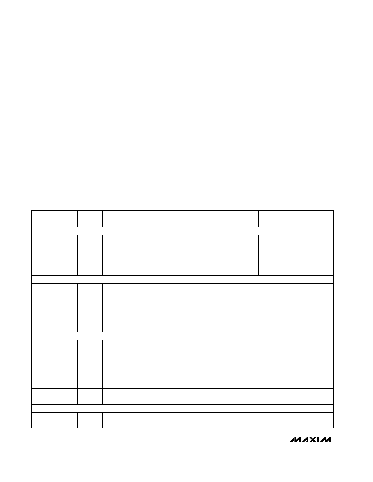
DC ELECTRICAL CHARACTERISTICS
(VCC= +3.0V to +3.6V, differential input voltage |VID| = 0.1V to 3.0V, input voltage (VIN, VIN) = 0 to VCC, input common-mode voltage
V
CM
= 0.05V to (VCC- 0.05V), LVPECL outputs terminated with 50Ω ±1% to (VCC- 2.0V), LVDS outputs terminated with 100Ω ±1%,
T
A
= -40°C to +85°C. Typical values are at VCC= +3.3V, |VID| = 0.2V, input common-mode voltage VCM= 1.2V, TA= +25°C, unless
otherwise noted.) (Notes 1, 2, 3)
PARAMETER SYMBOL CONDITIONS
LVCMOS/LVTTL INPUTS (RST, SEL)
Input High
Voltage
Input Low Voltage V
Input High Current I
Input Low Current I
DIFFERENTIAL INPUTS (IN, IN)
Differential Input
Threshold
V
V
IH
IL
THD
IH
IL
V
= V
IN
V
IL
or 2V 0 150 0 150 0 150 µA
CC
= 0 or 0.8V -20 +20 -20 +20 -20 +20 µA
MIN TYP MAX MIN TYP MAX MIN TYP MAX
2.0 V
GND 0.8 GND 0.8 GND 0.8 V
-100 ±6 +100 -100 ±6 +100 -100 ±6 +100 mV
-40°C +25°C +85°C
2.0 V
CC
2.0 V
CC
CC
UNITS
V
Input Current IIN, I INVIN, V IN = VCC or 0V -20 +20 -20 +20 -20 +20 µA
Input CommonMode Voltage
LVPECL OUTPUTS (OUT, OUT) (MAX9377)
Single-Ended
Output High
Voltage
Single-Ended
Output Low
Voltage
Differential Output
Voltage
LVDS OUTPUTS (OUT, OUT) (MAX9378)
Differential Output
Voltage
V
V
V
V
V
V
Figure 1 0.05
CM
Figure 3
OH
Figure 3
OL
-
OH
Figure 3 595 725 595 725 595 725 mV
OL
Figure 2 250 370 450 250 363 450 250 348 450 mV
OD
V
CC
1.085
V
CC
1.830
VCC -
0.992
VCC -
1.717
V
CC
0.05
VCC-
0.880
VCC -
1.620
-
0.05
VCC -
1.025
VCC -
1.810
V
-
CC
0.05
0.05
-
VCC -
VCC -
VCC -
1.033
0.880
1.025
-
VCC -
VCC -
VCC -
1.755
1.620
1.810
VCC -
0.978
VCC -
1.699
V
CC
0.05
VCC -
0.880
VCC -
1.620
V
V
V
MAX9377/MAX9378
Anything-to-LVPECL/LVDS Translators
with Pin-Selectable Divide-by-Four
_______________________________________________________________________________________ 3
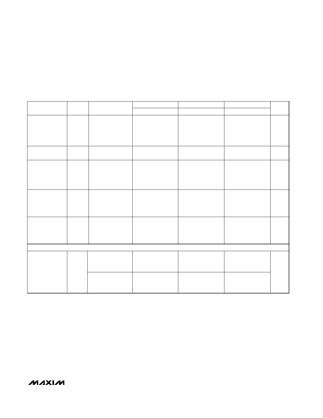
DC ELECTRICAL CHARACTERISTICS (continued)
(VCC= +3.0V to +3.6V, differential input voltage |VID| = 0.1V to 3.0V, input voltage (VIN, VIN) = 0 to VCC, input common-mode voltage
V
CM
= 0.05V to (VCC- 0.05V), LVPECL outputs terminated with 50Ω ±1% to (VCC- 2.0V), LVDS outputs terminated with 100Ω ±1%,
T
A
= -40°C to +85°C. Typical values are at VCC= +3.3V, |VID| = 0.2V, input common-mode voltage VCM= 1.2V, TA= +25°C, unless
otherwise noted.) (Notes 1, 2, 3)
PARAMETER SYMBOL CONDITIONS
Change in
Magnitude of V
Between
Complementary
Output States
Offset CommonMode Voltage
Change in
Magnitude of V
Between
Complementary
Output States
Output ShortCircuit Current,
Either Output
Shorted to GND
Output ShortCircuit Current,
Outputs Shorted
Together
POWER SUPPLY
Supply Current I
OD
∆V
Figure 2 1.0 20 1.0 20 1.0 20 mV
OD
V
Figure 2 1.125 1.375 1.125 1.250 1.375 1.125 1.375 V
OS
OS
∆VOS Figure 2 0.1 20 0.1 20 0.1 20 mV
= ±100mV, one
V
ID
output GND, other
I
OS
output open or
shorted to GND
V
= ±100mV,
ID
I
OSAB
CC
= V
V
OUT
MAX9377, all pins
open except V
GND
MAX9378, RL = 100,
quiescent, inputs are
open
OUT
CC
,
-40°C +25°C +85°C
MIN TYP MAX MIN TYP MAX MIN TYP MAX
19.0 24 19.0 24 19.0 24 mA
4.0 12 4.0 12 4.0 12 mA
13 22 15 22 17 22
18.0 30 20 30 22 30
UNITS
mA

MAX9377/MAX9378
Anything-to-LVPECL/LVDS Translators
with Pin-Selectable Divide-by-Four
4 _______________________________________________________________________________________
(
)
(
)
Note 1: Measurements are made with the device in thermal equilibrium. All voltages are referenced to ground except V
THD
, VID,
V
OD
, and ∆VOD.
Note 2: Current into a pin is defined as positive. Current out of a pin is defined as negative.
Note 3: DC parameters production tested at T
A
= +25°C and guaranteed by design and characterization over the full operating
temperature range.
Note 4: Guaranteed by design and characterization, not production tested. Limits are set at ±6 sigma.
Note 5: t
PCO
is the delay associated with the frequency-divider function. The total delay when divide-by-four is selected is t
PCO
+
t
PLH
.
Note 6: t
SKEW
is the magnitude difference of differential propagation delays for the same output under same conditions; t
SKEW
=
|t
PHL
- t
PLH
|.
Note 7: Device jitter added to the input signal.
AC ELECTRICAL CHARACTERISTICS
(VCC= +3.0V to +3.6V, differential input voltage |VID| = 0.1V to 1.2V, input frequency ≤ 1.34GHz, differential input transition time =
125ps (20% to 80%), input voltage (V
IN
, VIN) = 0 to VCC, input common-mode voltage VCM= 0.05V to (VCC- 0.05V), LVPECL outputs
terminated with 50Ω ±1% to (V
CC
- 2.0V) MAX9377, LVDS outputs terminated with RL= 100Ω ±1% (MAX9378), TA= -40°C to +85°C.
Typical values are at V
CC
= +3.3V, |VID| = 0.2V, input common-mode voltage VCM= 1.2V, TA= +25°C, unless otherwise noted.)
(Note 4)
PARAMETER SYMBOL CONDITIONS MIN TYP MAX UNITS
Reset-to-Differential Output Low
Delay
Reset-to-Input Clock Setup Time t
Clock-to-Divider Output
Propagation Delay
SEL to Switched Output Delay t
MAX9377
Switching Frequency f
Propagation Delay Low to High t
Propagation Delay High to Low t
Pulse Skew |t
PLH
-t
|t
PHL
Output Low-to-High Transition
Time (20% to 80%)
Output High-to-Low Transition
Time (20% to 80%)
Added Random Jitter t
MAX9378
Switching Frequency f
Propagation Delay Low to High t
Propagation Delay High to Low t
Pulse Skew |t
PLH
- t
|t
PHL
Output Low-to-High Transition
Time (20% to 80%)
Output High-to-Low Transition
Time (20% to 80%)
Added Random Jitter t
t
DR
SET
t
PCO
SEL
MAX
PLH
PHL
SKEW
t
t
RJ
MAX
PLH
PHL
SKEW
t
t
RJ
Figure 4 0.8 1.0 ns
Figure 4 0.5 ns
Figure 4 (Note 5) 0.6 1.0 ns
Figure 5 0.3 0.6 ns
VOH - VOL ≥ 250mV 2.0 2.5 GHz
Figure 3, SEL = 0 250 421 600 ps
Figure 3, SEL = 0 250 421 600 ps
(Note 6) 6 30 ps
Figure 3 116 220 ps
R
Figure 3 116 220 ps
F
fIN = 1.34GHz (Note 7), SEL = 0 0.7 2 ps
VOD ≥ 250mV 2.0 2.5 GHz
Figure 3, SEL = 0 250 363 600 ps
Figure 3, SEL = 0 250 367 600 ps
Figure 3 (Note 6) 3 30 ps
Figure 2 93 220 ps
R
Figure 2 93 220 ps
F
fIN = 1.34GHz (Note 7), SEL = 0 0.8 2 ps
RMS
RMS

MAX9377/MAX9378
Anything-to-LVPECL/LVDS Translators
with Pin-Selectable Divide-by-Four
_______________________________________________________________________________________ 5
Typical Operating Characteristics
(VCC= +3.3V, differential input voltage |VID| = 0.2V, VCM= 1.2V, input frequency = 500MHz, outputs terminated with 50Ω ±1% to
V
CC
- 2.0V (MAX9377), outputs terminated with 100Ω ±1% (MAX9378), TA= +25°C, unless otherwise noted.)
0
10
30
20
40
50
SUPPLY CURRENT vs. FREQUENCY
MAX9377/78 toc01
FREQUENCY (MHz)
SUPPLY CURRENT (mA)
0 1000500 1500 2000
MAX9378
MAX9377 NO LOAD
MAX9377
300
500
400
700
600
800
900
0 1000500 1500 2000
OUTPUT AMPLITUDE vs. FREQUENCY
MAX9377/78 toc02
FREQUENCY (MHz)
OUTPUT AMPLITUDE (mV)
MAX9378
MAX9377
300
360
340
320
380
400
420
440
460
480
500
-40 10-15 35 60 85
PROPAGATION DELAY
vs. TEMPERATURE
MAX9377/78 toc03
TEMPERATURE (°C)
PROPAGATION DELAY (ps)
t
PLH
(MAX9377)
t
PHL
(MAX9377)
t
PLH
(MAX9378)
t
PHL
(MAX9378)
70
90
80
110
100
130
120
140
-40 10-15 35 60 85
OUTPUT RISE/FALL TIME
vs. TEMPERATURE
MAX9377/78 toc04
TEMPERATURE (°C)
OUTPUT RISE/FALL TIME (ps)
tF (MAX9377)
tR (MAX9377)
tF (MAX9378)
tR (MAX9378)

MAX9377/MAX9378
Detailed Description
The MAX9377/MAX9378 are fully differential, highspeed, low-jitter anything-to-LVPECL and anything-toLVDS translators, respectively, with a selectable
divide-by-four function. Low propagation delay and
high speed make them ideal for various high-speed
network routing and backplane applications at speeds
up to 2GHz in nondivide mode.
The MAX9377/MAX9378 accept any differential input
signals within the supply rails and with a minimum
amplitude of 100mV. Inputs are fully compatible with
the LVDS, LVPECL, HSTL, and CML differential signaling standards. The MAX9377 outputs are LVPECL and
have sufficient current to drive 50Ω transmission lines.
The MAX9378 outputs are LVDS and conform to the
ANSI EIA/TIA-644 LVDS standard.
Inputs
Inputs have a wide common-mode range of 0.05V to
(VCC- 0.05V), which accommodates any differential signals within the supply rails, and requires a minimum of
100mV to switch the outputs. This allows the
MAX9377/MAX9378 inputs to support virtually any differential signaling standard.
RST and SEL Inputs
The frequency-divide functions are controlled by two
LVCMOS/LVTTL inputs, RST and SEL. SEL selects
either the divide-by-four function or a no-division function as shown in Table 1. RST, an asynchronous activehigh input, resets the divide-by-four within the device
and places the circuits into a known state. Setting RST
high when powering up the device with SEL high prevents the unknown states with the divider from being
propagated to the outputs. If the device is powered up
with SEL high but without asserting RST, the outputs
are only guaranteed to be 1/4th the input frequency
after 2.5 cycles have been applied to the input.
LVPECL Outputs (MAX9377)
The MAX9377 LVPECL outputs are emitter followers
that require external resistive paths to a voltage source
(VT= VCC- 2.0V typ) more negative than worst-case
VOLfor proper static and dynamic operation. When
properly terminated, the outputs generate steady-state
voltage levels, VOLor VOHwith fast transition edges
between state levels. Output current always flows into
the termination during proper operation.
LVDS Outputs (MAX9378)
The MAX9378 LVDS outputs require a resistive load to
terminate the signal and complete the transmission
loop. Because the device switches current and not voltage, the actual output voltage swing is determined by
the value of the termination resistor. With a 3.5mA typical output current, the MAX9378 produces an output
voltage of 350mV when driving a 100Ω load.
Anything-to-LVPECL/LVDS Translators
with Pin-Selectable Divide-by-Four
6 _______________________________________________________________________________________
Pin Description
Table 1. SEL AND RST Truth Table
PIN NAME FUNCTION
1 SEL
2 IN Differential LVDS/Any Noninverting Input
3 IN Differential LVDS/Any Inverting Input
4 GND Ground
5 RST Frequency Divider Reset Input. Active high, asynchronous, reset. Internal 75kΩ pulldown to GND.
6 OUT
7 OUT
8V
CC
Frequency Divider Select Input. High = divide by four, low = no division. Internal 75kΩ pulldown to
GND.
MAX9377 Differential LVPECL Inverting Output. Terminate with 50Ω ±1% to VCC - 2V.
MAX9378 Inverting LVDS Output. Terminate to OUT with 100Ω ±1%.
MAX9377 Differential LVPECL Noninverting Output. Terminate with 50Ω ±1% to VCC - 2V.
MAX9378 Noninverting LVDS Output. Terminate to OUT with 100Ω ±1%.
Positive Supply. Bypass from VCC to GND with 0.1µF and 0.01µF ceramic capacitors. Place the
capacitors as close to the device as possible with the smaller value capacitor closest to the device
RST SEL OUTPUT
X L or open No frequency division.
H H Outputs are placed in differential low.
L H Divide-by-four function.

Applications Information
LVPECL Output Termination (MAX9377)
Terminate the MAX9377 LVPECL outputs with 50Ω to
(VCC- 2V) or use equivalent Thevenin terminations.
Terminate OUT and OUT with identical termination on
each for low output distortion. When a single-ended
signal is taken from the differential output, terminate
both OUT and OUT. Ensure that output currents do not
exceed the current limits as specified in the Absolute
Maximum Ratings. Under all operating conditions, the
device’s total thermal limits should be observed.
LVDS Output Termination (MAX9378)
The MAX9378 LVDS outputs are current-steering
devices; no output voltage is generated without a termination resistor. The termination resistors should match
the differential impedance of the transmission line.
Output voltage levels are dependent upon the value of
the termination resistor. The MAX9378 is optimized for
point-to-point communication with the 100Ω termination
resistor at the receiver inputs. Termination resistance
values may range between 90Ω and132Ω, depending
on the characteristic impedance of the transmission
medium.
Supply Bypassing
Bypass VCCto ground with high-frequency surfacemount ceramic 0.1µF and 0.01µF capacitors. Place the
capacitors as close to the device as possible with the
0.01µF capacitor closest to the device pins.
Traces
Circuit board trace layout is very important to maintain
the signal integrity of high-speed differential signals.
Maintaining integrity is accomplished in part by reducing signal reflections and skew, and increasing common-mode noise immunity.
Signal reflections are caused by discontinuities in the
50Ω characteristic impedance of the traces. Avoid discontinuities by maintaining the distance between differential traces, not using sharp corners or using vias.
Maintaining distance between the traces also increases
common-mode noise immunity. Reducing signal skew
is accomplished by matching the electrical length of
the differential traces.
MAX9377/MAX9378
Anything-to-LVPECL/LVDS Translators
with Pin-Selectable Divide-by-Four
_______________________________________________________________________________________ 7
Figure 1. Differential Input Definition
Figure 2. LVDS Output Load and Transition Times
Figure 3. Differential Input-to-Output Propagation Delay Timing
Diagram
V
CC
GND
V
ID
V
ID
VCM (MAX) = VCC - 0.05V
VCM (MIN) = 0.05V
/ 2
R
VOD
80%
L
R
/ 2
L
t
F
VOS
GND
0V
20%
OUT - OUT
DRV
VOD(-)
C
20%
OUT
OUT
L
C
L
VOD(+)
80%
t
R
IN
OR (VIH - VIL)
IN
OUT
OUT
DIFFERENTIAL OUTPUT
WAVEFORM
OUT - OUT
20%
V
ID
t
PLH
VOD OR (VOH - VOL)
80%
+VOD OR +(VOH - VOL)
-VOD OR -(VOH - VOL)
t
R
0V DIFFERENTIAL
t
PHL
80%
0V DIFFERENTIAL
t
F
20%
V
OH
V
OL

MAX9377/MAX9378
Anything-to-LVPECL/LVDS Translators
with Pin-Selectable Divide-by-Four
8 _______________________________________________________________________________________
Figure 4. Frequency Divider and Reset Timing Diagram
Figure 5. Frequency Select Delay Timing Diagram
Chip Information
MAX9377 TRANSISTOR COUNT: 614
MAX9378 TRANSISTOR COUNT: 614
PROCESS: Bipolar
1 OUT
4 OUT
RST
IN
t
DR
t
PLH
t
PCO
t
SET
IN
IN/4
t
PCO
SEL
OUT
t
SEL

MAX9377/MAX9378
Anything-to-LVPECL/LVDS Translators
with Pin-Selectable Divide-by-Four
Maxim cannot assume responsibility for use of any circuitry other than circuitry entirely embodied in a Maxim product. No circuit patent licenses are
implied. Maxim reserves the right to change the circuitry and specifications without notice at any time.
Maxim Integrated Products, 120 San Gabriel Drive, Sunnyvale, CA 94086 408-737-7600 _____________________ 9
© 2003 Maxim Integrated Products Printed USA is a registered trademark of Maxim Integrated Products.
Package Information
(The package drawing(s) in this data sheet may not reflect the most current specifications. For the latest package outline information,
go to www.maxim-ic.com/packages
.)
b
E H
A1
4X S
BOTTOM VIEW
A
c
L
SIDE VIEW
8
1
DIM
A
A1
A2
b
c
D
e
E
H
L
α
S
INCHES
MIN
-
0.002
0.030
0.010
0.005
0.116
0.0256 BSC
0.116
0.188
0.016
0∞
0.0207 BSC
MAX
0.043
0.006
0.037
0.014
0.007
0.120
0.120
0.198
0.026
6∞
MILLIMETERS
MIN
0.05 0.15
0.25 0.36
0.13 0.18
2.95 3.05
2.95 3.05
4.78
0.41
MAX
- 1.10
0.950.75
0.65 BSC
5.03
0.66
6∞0∞
0.5250 BSC
α
8
ÿ 0.50±0.1
0.6±0.1
0.6±0.1
1
D
TOP VIEW
A2
e
FRONT VIEW
8LUMAXD.EPS
PROPRIETARY INFORMATION
TITLE:
PACKAGE OUTLINE, 8L uMAX/uSOP
REV.DOCUMENT CONTROL NO.APPROVAL
21-0036
1
J
1
 Loading...