

Page 1
General Description
The MAX9376 is a fully differential, high-speed,
LVDS/anything-to-LVPECL/LVDS dual translator
designed for signal rates up to 2GHz. One channel is
LVDS/anything-to-LVPECL translator and the other
channel is LVDS/anything-to-LVDS translator. The
MAX9376’s extremely low propagation delay and high
speed make it ideal for various high-speed network
routing and backplane applications.
The MAX9376 accepts any differential input signal within the supply rails and with minimum amplitude of
100mV. Inputs are fully compatible with the LVDS,
LVPECL, HSTL, and CML differential signaling standards. LVPECL outputs have sufficient current to drive
50Ω transmission lines. LVDS outputs conform to the
ANSI EIA/TIA-644 LVDS standard.
The MAX9376 is available in a 10-pin µMAX
®
package
and operates from a single +3.3V supply over the -40°C
to +85°C temperature range.
Applications
Backplane Logic Standard Translation
LVDS-to-LVPECL, LVPECL-to-LVDS
Up/Downconverters
LANs
WANs
DSLAMs
DLCs
Features
o Guaranteed 2GHz Switching Frequency
o Accepts LVDS/LVPECL/Anything Inputs
o 421ps (typ) Propagation Delays
o 30ps (max) Pulse Skew
o 2ps
RMS
(max) Random Jitter
o Minimum 100mV Differential Input to Guarantee
AC Specifications
o Temperature-Compensated LVPECL Output
o +3.0V to +3.6V Power-Supply Operating Range
o >2kV ESD Protection (Human Body Model)
MAX9376
LVDS/Anything-to-LVPECL/LVDS Dual Translator
________________________________________________________________
Maxim Integrated Products
1
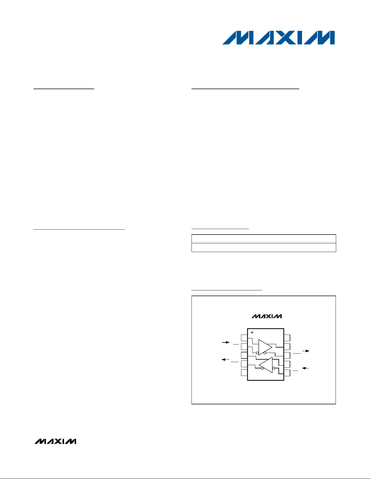
Pin Configuration
Ordering Information
19-2809; Rev 1; 10/09
For pricing, delivery, and ordering information, please contact Maxim Direct at 1-888-629-4642,
or visit Maxim’s website at www.maxim-ic.com.
Functional Diagram appears at end of data sheet.
+
Denotes a lead(Pb)-free/RoHS-compliant package.
µMAX is a registered trademark of Maxim Integrated Products, Inc.
PART TEMP RANGE PIN-PACKAGE
MAX9376EUB+ -40°C to +85°C 10 µMAX
TOP VIEW
ANYTHING
LVDS
IN1
IN1
OUT2
MAX9376
1
2
3
4
5
μMAX
10
9
8
7
6
V
CC
OUT1
OUT1
IN2OUT2
IN2GND
LVPECL
ANYTHING
Page 2
MAX9376
LVDS/Anything-to-LVPECL/LVDS Dual Translator
2 _______________________________________________________________________________________
ABSOLUTE MAXIMUM RATINGS
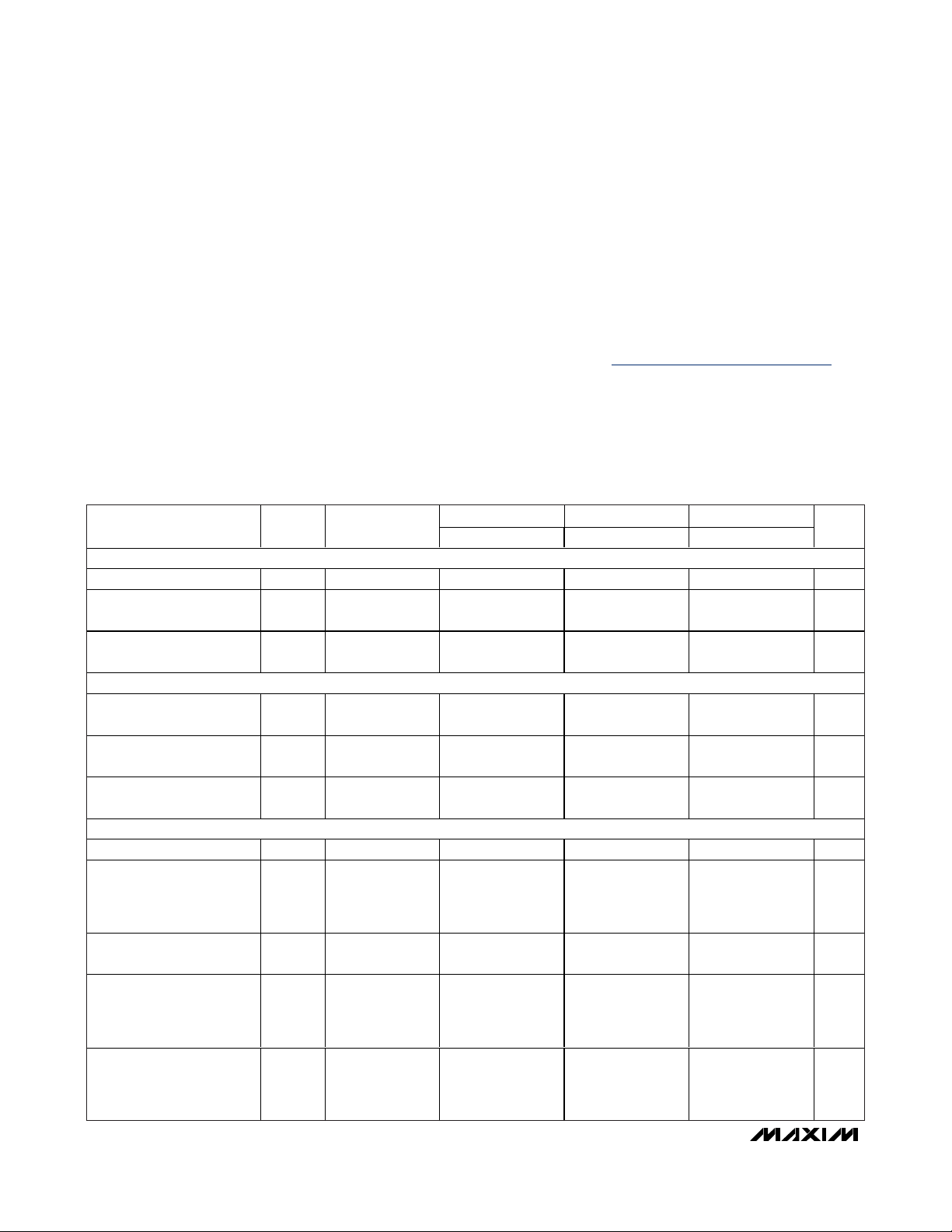
DC ELECTRICAL CHARACTERISTICS
(VCC= +3.0V to +3.6V, differential input voltage |VID| = 0.1V to 3.0V, input voltage (VIN, VIN) = 0 to VCC, input common-mode voltage
V
CM
= 0.05V to (VCC- 0.05V), LVPECL outputs terminated with 50Ω ±1% to (VCC- 2.0V), LVDS outputs terminated with 100Ω ±1%,
T
A
= -40°C to +85°C. Typical values are at VCC= +3.3V, |VID| = 0.2V, input common-mode voltage VCM= 1.2V, TA= +25°C, unless
otherwise noted.) (Notes 2, 3, 4)
Stresses beyond those listed under “Absolute Maximum Ratings” may cause permanent damage to the device. These are stress ratings only, and functional
operation of the device at these or any other conditions beyond those indicated in the operational sections of the specifications is not implied. Exposure to
absolute maximum rating conditions for extended periods may affect device reliability.
VCCto GND...........................................................-0.3V to +4.1V
Inputs (IN_, IN_) .........................................-0.3V to (V
CC
+ 0.3V)
IN to IN ................................................................................±3.0V
Continuous Output Current .................................................50mA
Surge Output Current .......................................................100mA
Continuous Power Dissipation (T
A
= +70°C)
10-Pin µMAX (derate 5.6mW/°C above +70°C) ..........444mW
θ
JA
in Still Air (Note 1) ............................................+180°C/W
Junction Temperature......................................................+150°C
Storage Temperature Range .............................-65°C to +150°C
ESD Protection
Human Body Model (IN_, IN_, OUT_, OUT_) ..................≥2kV
Soldering Temperature (10s) ...........................................+300°C
Note 1: Package thermal resistances were obtained using the method described in JEDEC specification JESD51-7, using a four-
layer board. For detailed information on package thermal considerations, refer to www.maxim-ic.com/thermal-tutorial
.
PARAMETER SYMBOL CONDITIONS
DIFFERENTIAL INPUTS (IN_, IN_ )
Differential Input Threshold V
Input Current
Input Common-Mode
Voltage
I
V
THD
,
VIN, V
IN
I
V
IN
Figure 1 0.05
CM
LVPECL OUTPUTS (OUT1, OUT1)
Single-Ended Output High
Voltage
Single-Ended Output Low
Voltage
Differential Output Voltage
V
V
V
OH
V
Figure 3
OH
Figure 3
OL
Figure 3 595 710 595 710 595 710 mV
OL
LVDS OUTPUTS (OUT2, OUT2 )
Differential Output Voltage V
Figure 2 250 366 450 250 352 450 250 339 450 mV
OD
Change in Magnitude of
Between
V
OD
Complementary Output
| Figure 2 1.0 20 1.0 20 1.0 20 mV
|ΔV
OD
States
Offset Common-Mode
Voltage
V
Figure 2 1.125 1.375 1.125 1.250 1.375 1.125 1.375 V
OS
Change in Magnitude of
Between
V
OS
Complementary Output
| Figure 2 1.0 20 1.0 20 1.0 20 mV
|ΔV
OS
States
Output Short-Circuit
Current, Either Output
Shorted to GND
|I
V
one outp ut GN D ,
|
OS
other outp ut op en
or shor ted to G N D
IN
or 0V
CC
= ± 100m V ,
ID
=
MIN TYP MAX MIN TYP MAX MIN TYP MAX
-100 +100 -100 +100 -100 +100 mV
-20 +20 -20 +20 -20 +20 µA
V
-
CC
1.085
V
-
CC
1.830
-40°C +25°C +85°C
V
VCC -
1.035
VCC -
1.745
CC
0.05
VCC -
0.880
VCC -
1.620
-
0.05
VCC -
1.025
VCC -
1.810
VCC -
0.985
VCC -
1.694
VCC -
0.05
VCC -
0.880
VCC -
1.620
0.05
VCC -
1.025
VCC -
1.810
VCC -
0.976
VCC -
1.681
VCC -
0.05
VCC -
0.880
VCC -
1.620
19 24 18 24 18 24 mA
UNITS
V
V
V
Page 3
MAX9376
LVDS/Anything-to-LVPECL/LVDS Dual Translator
_______________________________________________________________________________________ 3
AC ELECTRICAL CHARACTERISTICS
(VCC= +3.0V to +3.6V, differential input voltage |VID| = 0.1V to 1.2V, input frequency ≤ 1.34GHz, differential input transition time =
125ps (20% to 80%), input voltage (V
IN
, VIN) = 0 to VCC, input common-mode voltage (VCM) = 0.05V to (VCC- 0.05V), LVPECL out-
puts terminated with 50Ω ±1% to (V
CC
- 2.0V), LVDS outputs terminated with 100Ω ±1%, TA = -40°C to +85°C. Typical values are at
V
CC
= +3.3V, |VID| = 0.2V, input common-mode voltage VCM= 1.2V, TA= +25°C, unless otherwise noted.) (Note 5)
(
)
DC ELECTRICAL CHARACTERISTICS (continued)
(VCC= +3.0V to +3.6V, differential input voltage |VID| = 0.1V to 3.0V, input voltage (VIN, VIN) = 0 to VCC, input common-mode voltage
V
CM
= 0.05V to (VCC- 0.05V), LVPECL outputs terminated with 50Ω ±1% to (VCC- 2.0V), LVDS outputs terminated with 100Ω ±1%,
T
A
= -40°C to +85°C. Typical values are at VCC= +3.3V, |VID| = 0.2V, input common-mode voltage VCM= 1.2V, TA= +25°C, unless
otherwise noted.) (Notes 2, 3, 4)
-40°C +25°C +85°C
PARAMETER
SYMBOL
CONDITIONS
UNITS
Output Short-circuit
Current, Outputs Shorted
Together
VID = ±100mV,
SUPPLY
Supply Current I
CC
All pins open
except V
CC
and
GND with LVDS
outputs (OUT2,
OUT2) loaded
with differential
100Ω
LVPECL OUTPUTS
Switching Frequency f
Propagation Delay Low to High t
Propagation Delay High to Low t
Pulse Skew |t
Output Low-to-High Transition
Output High-to-Low Transition
Added Random Jitter t
LVDS OUTPUTS
Switching Frequency f
Propagation Delay Low to High t
Propagation Delay High to Low t
Pulse Skew |t
Output Low-to-High Transition
Time (20% to 80%)
Output High-to-Low Transition
Time (20% to 80%)
PARAMETER SYMBOL CONDITIONS MIN TYP MAX UNITS
PLH
PLH
MIN TYP MAX MIN TYP MAX MIN TYP MAX
|I
OSAB
|
V
OUT
_+ = V
OUT
_-
4.0 12 4.0 12 4.0 12 mA
24 40 29 40 31 40 mA
- t
|t
PHL
- t
|t
PHL
MAX
PLH
PHL
SKEW
t
R
t
F
RJ
MAX
PLH
PHL
SKEW
t
R
VOH - V
Figure 3 250 421 600 ps
Figure 3 250 421 600 ps
Figure 3 (Note 6) 6 30 ps
Figure 3 116 220 ps
Figure 3 119 220 ps
fIN = 1.34GHz (Note 7) 0.7 2 ps
VOD ≥ 250mV 2.0 2.5 GHz
Figure 3 250 363 600 ps
Figure 3 250 367 600 ps
Figure 3 (Note 6) 5 30 ps
Figure 2 93 220 ps
≥ 250mV 2.0 2.5 GHz
OL
t
Figure 2 91 220 ps
F
RMS
Page 4

MAX9376
LVDS/Anything-to-LVPECL/LVDS Dual Translator
4 _______________________________________________________________________________________
Typical Operating Characteristics
(VCC= +3.3V, differential input voltage |VID| = 0.2V, VCM= 1.2V, input frequency = 500MHz, LVPECL outputs terminated with 50Ω
±1% to V
CC
- 2.0V, LVDS outputs terminated with 100Ω ±1%, TA= +25°C, unless otherwise noted.)
AC ELECTRICAL CHARACTERISTICS (continued)
(VCC= +3.0V to +3.6V, differential input voltage |VID| = 0.1V to 1.2V, input frequency ≤ 1.34GHz, differential input transition time =
125ps (20% to 80%), input voltage (V
IN
, VIN) = 0 to VCC, input common-mode voltage (VCM) = 0.05V to (VCC- 0.05V), LVPECL out-
puts terminated with 50Ω ±1% to (V
CC
- 2.0V), LVDS outputs terminated with 100Ω ±1%, TA = -40°C to +85°C. Typical values are at
V
CC
= +3.3V, |VID| = 0.2V, input common-mode voltage VCM= 1.2V, TA= +25°C, unless otherwise noted.) (Note 5)
(
)
Note 2: Measurements are made with the device in thermal equilibrium. All voltages are referenced to ground except V
THD
, VID,
V
OD
, and ΔVOD.
Note 3: Current into a pin is defined as positive. Current out of a pin is defined as negative.
Note 4: DC parameters production tested at T
A
= +25°C and guaranteed by design and characterization over the full operating
temperature range.
Note 5: Guaranteed by design and characterization, not production tested. Limits are set at ±6 sigma.
Note 6: t
SKEW
is the magnitude difference of differential propagation delays for the same output under same conditions; t
SKEW
=
|t
PHL
- t
PLH
|.
Note 7: Device jitter added to the input signal.
PARAMETER SYMBOL CONDITIONS MIN TYP MAX UNITS
Added Random Jitter t
RJ
fIN = 1.34GHz (Note 7) 0.8 2 ps
RMS
SUPPLY CURRENT
vs. FREQUENCY
50
LVPECL OUTPUTS
UNLOADED
40
30
20
SUPPLY CURRENT (mA)
10
0
02000
FREQUENCY (MHz)
15001000500
MAX9376 toc01
900
800
700
600
500
OUTPUT AMPLITUDE (mV)
400
300
02000
PROPAGATION DELAY
vs. TEMPERATURE
500
480
460
t
(LVPECL)
PLH
440
420
400
380
360
PROPAGATION DELAY (ps)
340
320
300
-40 85
t
(LVPECL)
PHL
t
t
PHL
TEMPERATURE (°C)
PLH
(LVDS)
MAX9376 toc03
(LVDS)
603510-15
140
130
120
110
100
90
OUTPUT RISE/FALL TIME (ps)
80
70
-40 85
OUTPUT AMPLITUDE
vs. FREQUENCY
LVPECL
LVDS
15001000500
FREQUENCY (MHz)
OUTPUT RISE/FALL TIME
vs. TEMPERATURE
tF (LVPECL)
tR (LVPECL)
tF (LVDS)
tR (LVPECL)
603510-15
TEMPERATURE (°C)
MAX9376 toc02
MAX9376 toc04
Page 5

MAX9376
LVDS/Anything-to-LVPECL/LVDS Dual Translator
_______________________________________________________________________________________ 5
Pin Description
Detailed Description
The MAX9376 is a fully differential, high-speed,
LVDS/anything-to-LVPECL/LVDS dual translator
designed for signal rates up to 2GHz. One channel is
LVDS/anything-to-LVPECL translator and the other
channel is LVDS/anything-to-LVDS translator. The
MAX9376’s extremely low propagation delay and high
speed make it ideal for various high-speed network
routing and backplane applications.
The MAX9376 accepts any differential input signal within the supply rails and with a minimum amplitude of
100mV. Inputs are fully compatible with the LVDS,
LVPECL, HSTL, and CML differential signaling standards. LVPECL outputs have sufficient current to drive
50Ω transmission lines. LVDS outputs conform to the
ANSI EIA/TIA-644 LVDS standard.
Inputs
Inputs have a wide common-mode range of 0.05V to
VCC- 0.05V, which accommodates any differential signals within rails, and requires a minimum of 100mV to
switch the outputs. This allows the MAX9376 inputs to
support virtually any differential signaling standard.
LVPECL Outputs
The MAX9376 LVPECL outputs are emitter followers
that require external resistive paths to a voltage source
(VT = VCC- 2.0V typ) more negative than worst-case
VOLfor proper static and dynamic operation. When
properly terminated, the outputs generate steady-state
voltage levels, VOLor VOHwith fast transition edges
between state levels. Output current always flows into
the termination during proper operation.
LVDS Outputs
The MAX9376 LVDS outputs require a resistive load to
terminate the signal and complete the transmission
loop. Because the device switches current and not voltage, the actual output voltage swing is determined by
the value of the termination resistor. With a 3.5mA typical output current, the MAX9376 produces an output
voltage of 350mV when driving a 100Ω load.
PIN NAME FUNCTION
1 IN1 Differential LVDS/Anything Noninverting Input 1
2 IN1 Differential LVDS/Anything Inverting Input 1
3 OUT2 Differential LVDS Noninverting Output 2. Terminate with 100Ω ±1% to OUT2.
4 OUT2 Differential LVDS Inverting Output 2. Terminate with 100Ω ±1% to OUT2.
5 GND Ground
6 IN2 Differential LVDS/Anything Inverting Input 2
7 IN2 Differential LVDS/Anything Noninverting Input 2
8 OUT1 Differential LVPECL Inverting Output. Terminate with 50Ω ±1% to VCC - 2V.
9 OUT1 Differential LVPECL Noninverting Output. Terminate with 50Ω ±1% to VCC - 2V.
Positive Supply. Bypass from VCC to GND with 0.1µF and 0.01µF ceramic capacitors. Place
10 V
CC
the capacitors as close to the device as possible with the smaller value capacitor closest to
the device.
Page 6

MAX9376
LVDS/Anything-to-LVPECL/LVDS Dual Translator
6 _______________________________________________________________________________________
Applications Information
LVPECL Output Termination
Terminate the MAX9376 LVPECL outputs with 50Ω to
(V
CC
- 2V) or use equivalent Thevenin terminations.
Terminate OUT1 and OUT1 with identical termination
on each for low output distortion. When a single-ended
signal is taken from the differential output, terminate
both OUT1 and OUT1.
Ensure that output currents do not exceed the current
limits as specified in the
Absolute Maximum Ratings
.
Under all operating conditions, the device’s total thermal limits should be observed.
LVDS Output Termination
The MAX9376 LVDS outputs are current-steering
devices; no output voltage is generated without a termination resistor. The termination resistors should match
the differential impedance of the transmission line.
Output voltage levels are dependent upon the value of
the termination resistor. The MAX9376 is optimized for
point-to-point interface with 100Ω termination resistors
at the receiver inputs. Termination resistance values
may range between 90Ω and132Ω, depending on the
characteristic impedance of the transmission medium.
Supply Bypassing
Bypass VCCto ground with high-frequency surfacemount ceramic 0.1µF and 0.01µF capacitors. Place the
capacitors as close to the device as possible with the
0.01µF capacitor closest to the device pins.
Traces
Circuit board trace layout is very important to maintain
the signal integrity of high-speed differential signals.
Maintaining integrity is accomplished in part by reducing signal reflections and skew, and increasing common-mode noise immunity.
Signal reflections are caused by discontinuities in the
50Ω characteristic impedance of the traces. Avoid discontinuities by maintaining the distance between differential traces, not using sharp corners or using vias.
Maintaining distance between the traces also increases
common-mode noise immunity. Reducing signal skew
is accomplished by matching the electrical length of
the differential traces.
Figure 1. Input Definition
Figure 2. LVDS Output Load and Transition Times
Figure 3. Differential Input-to-Output Propagation Delay Timing
Diagram
V
CC
V
ID
V
ID
GND
OUT2
80%
C
L
VOD(+)
VOD
DRV
VOD(-)
OUT2 - OUT2
C
L
20%
OUT2
t
R
IN
OR (VIH - VIL)
V
ID
IN
t
PLH
OUT
VOD OR (VOH - VOL)
OUT
80%
+VOD OR +(VOH - VOL)
DIFFERENTIAL OUTPUT
WAVEFORM
OUT - OUT
20%
-VOD OR -(VOH - VOL)
t
R
VCM (MAX)
VCM (MIN)
/ 2
R
L
R
/ 2
L
GND
80%
t
F
0V DIFFERENTIAL
t
PHL
80%
0V DIFFERENTIAL
t
F
20%
20%
V
V
VOS
0V
OH
OL
Page 7

MAX9376
LVDS/Anything-to-LVPECL/LVDS Dual Translator
_______________________________________________________________________________________ 7
Chip Information
PROCESS: Bipolar
Package Information
For the latest package outline information and land patterns, go
to www.maxim-ic.com/packages
. Note that a “+”, “#”, or “-” in
the package code indicates RoHS status only. Package drawings may show a different suffix character, but the drawing pertains to the package regardless of RoHS status.
PACKAGE TYPE PACKAGE CODE DOCUMENT NO.
10µMAX U10+2
21-0061
Page 8

MAX9376
LVDS/Anything-to-LVPECL/LVDS Dual Translator
Maxim cannot assume responsibility for use of any circuitry other than circuitry entirely embodied in a Maxim product. No circuit patent licenses are
implied. Maxim reserves the right to change the circuitry and specifications without notice at any time.
8
_____________________Maxim Integrated Products, 120 San Gabriel Drive, Sunnyvale, CA 94086 408-737-7600
© 2009 Maxim Integrated Products Maxim is a registered trademark of Maxim Integrated Products, Inc.
Revision History
REVISION
NUMBER
0 4/03 Initial release —
1 10/09 Updated Ordering Information and Absolute Maximum Ratings 1, 2
REVISION
DATE
DESCRIPTION
PAGES
CHANGED
 Loading...