

Page 1
General Description
The MAX9370/MAX9371/MAX9372 LVTTL/TTL-to-differential LVPECL/PECL translators are designed for highspeed communication signal and clock driver
applications. The MAX9370/MAX9372 are dual
LVTTL/TTL-to-LVPECL/PECL translators that operate in
excess of 1GHz. The MAX9371 is a single translator.
The MAX9370/MAX9371 operate over a wide 3.0V to
5.25V supply range, allowing high-performance clock
or data distribution in systems with a nominal 3.3V or
5.0V supply. The MAX9372 is designed to operate from
3.0V to 3.6V.
The devices default to output high if the input is disconnected. They feature low 270ps propagation delay. The
MAX9370/MAX9371/MAX9372 employ industry-standard flow-through pinouts. These devices are specified
for operation from -40°C to +85°C, and are offered in
space-saving, 8-pin SOT23, µMAX, and SO packages.
Applications
Precision Clock/Data Level Translation
Central Office Clock Distribution
DSLAM/DLC
Base Station
Mass Storage
Features
♦ Guaranteed 1GHz Operating Frequency at 600mV
Differential Output
♦ 270ps Propagation Delay
♦ 10ps Output-to-Output Skew (MAX9370/MAX9372)
♦ Wide Supply Range: 3.0V to 5.25V
(MAX9370/MAX9371)
♦ ESD Protection > 2kV (Human Body Model)
♦ Output High with Input Open
♦ Available in Small 8-Pin SOT23, µMAX, and SO
Packages
♦ Improved Upgrades to MC100EL22, MC100EPT20,
MC100EPT22
MAX9370/MAX9371/MAX9372
LVTTL/TTL-to-Differential LVPECL/PECL
Translators
________________________________________________________________ Maxim Integrated Products 1
Ordering Information
MAX9370
MAX9371
MAX9372
TTL/LVTTL
INPUT
Q_
D
Q_
Z
0
= 50Ω
Z
0
= 50Ω
50Ω
50Ω
PECL/LVPECL
RECEIVER
VCC - 2.0V
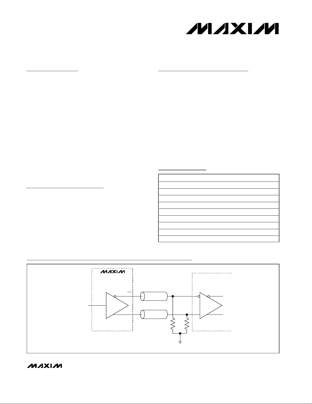
Typical Operating Circuit
19-2377; Rev 0; 4/02
For pricing, delivery, and ordering information, please contact Maxim/Dallas Direct! at
1-888-629-4642, or visit Maxim’s website at www.maxim-ic.com.
PART TEMP RANGE PIN-PACKAGE
MAX9370EKA-T* -40°C to +85°C 8 SOT23-8
MAX9370EUA* -40°C to +85°C 8 µMAX
MAX9370ESA -40°C to +85°C 8 SO
MAX9371EKA-T* -40°C to +85°C 8 SOT23-8
MAX9371EUA* -40°C to +85°C 8 µMAX
MAX9371ESA -40°C to +85°C 8 SO
MAX9372EKA-T* -40°C to +85°C 8 SOT23-8
MAX9372EUA* -40°C to +85°C 8 µMAX
MAX9372ESA -40°C to +85°C 8 SO
*Future product—contact factory for availability.
Pin Configurations/Functional Diagrams appears at end of
data sheet.
Page 2
MAX9370/MAX9371/MAX9372
LVTTL/TTL-to-Differential LVPECL/PECL
Translators
2 _______________________________________________________________________________________
ABSOLUTE MAXIMUM RATINGS
Stresses beyond those listed under “Absolute Maximum Ratings” may cause permanent damage to the device. These are stress ratings only, and functional
operation of the device at these or any other conditions beyond those indicated in the operational sections of the specifications is not implied. Exposure to
absolute maximum rating conditions for extended periods may affect device reliability.
VCCto GND (MAX9370/MAX9371) .......................-0.3V to +5.5V
V
CC
to GND (MAX9372)........................................-0.3V to +4.0V
D_ to GND ..................................................-0.3V to (V
CC
+ 0.3V)
Q_,
Q_ to GND ...........................................-0.3V to (VCC+ 0.3V)
Continuous Output Current ................................................50mA
Surge Output Current........................................................100mA
Junction-to-Ambient Thermal Resistance in Still Air
8-Pin SOT23..............................................................+112°C/W
8-Pin µMAX…............................................................+221°C/W
8-Pin SO....................................................................+170°C/W
Junction-to-Ambient Thermal Resistance with
500LFPM Airflow
8-Pin SOT23................................................................+78°C/W
8-Pin µMAX…............................................................+155°C/W
8-Pin SO......................................................................+99°C/W
Junction-to-Case Thermal Resistance
8-Pin SOT23................................................................+80°C/W
8-Pin µMAX…..............................................................+39°C/W
8-Pin SO......................................................................+40°C/W
Continuous Power Dissipation (T
A
= +70°C)
8-Pin SO (derate 5.9mW/°C above +70°C)...................470mW
8-Pin µMAX (derate 4.5mW/°C above +70°C) ..............362mW
8-Pin SOT23 (derate 8.9mW/°C above +70°C).............714mW
Operating Temperature Range ...........................-40°C to +85°C
Junction Temperature .....................................................+150°C
Storage Temperature Range .............................-60°C to +150°C
Soldering Temperature (10s) ...........................................+300°C
DC ELECTRICAL CHARACTERISTICS
(VCC= 3.0V to 5.25V for MAX9370/MAX9371, VCC= 3.0V to 3.6V for MAX9372, outputs terminated with 50Ω ±1% to VCC- 2.0V.
Typical values are at V
CC
= 3.3V, V
IH
= 2.4V, VIL= 0.4V, unless otherwise noted.) (Notes 1, 2, 3)
-40°C +25°C +85°C
PARAMETER
SYMBOL
CONDITIONS
UNITS
LVTTL INPUTS (D_)
Input High
Voltage
V
IH
V
Input Low
Voltage
V
IL
V
Input Low
Current
I
IL
VD = 0.5V
µA
VD = 2.7V
VD = VCC,
MAX9370/
MAX9371
Input High
Current
I
IH
VD = VCC,
MAX9372
20 20 20
µA
Input Clamp
Voltage
V
LVPECL/PECL OUTPUTS (Q_, Q_)
MAX9370
Output High
Voltage
V
OH
MAX9371/
MAX9372
V
MAX9370
Output Low
Voltage
V
OL
MAX9371/
MAX9372
V
MIN TYP MAX MIN TYP MAX MIN TYP MAX
2.0 2.0 2.0
IIL or IIH = 18mA -1.2 -1.2 -1.2
-50 +10 -50 +10 -50 +10
V
-
CC
1.085
V
-
CC
1.145
V
-
CC
1.83
V
-
CC
1.945
0.8 0.8 0.8
-100 -100 -100
130 130 130
V
-
V
CC
0.895
V
CC
0.895
V
CC
1.62
V
CC
1.695
-
CC
1.025
-
V
-
CC
1.145
-
V
-
CC
1.81
-
V
-
CC
1.945
V
CC
0.895
V
CC
0.895
V
CC
1.62
V
CC
-1.695
-
V
-
CC
1.025
-
V
-
CC
1.145
-
V
-
CC
1.81
-
V
-
CC
1.945
V
CC
0.895
V
CC
0.895
V
CC
1.62
V
CC
1.695
-
-
-
-
Page 3
MAX9370/MAX9371/MAX9372
LVTTL/TTL-to-Differential LVPECL/PECL
Translators
_______________________________________________________________________________________ 3
DC ELECTRICAL CHARACTERISTICS (continued)
(VCC= 3.0V to 5.25V for MAX9370/MAX9371, VCC= 3.0V to 3.6V for MAX9372, outputs terminated with 50Ω ±1% to VCC- 2.0V.
Typical values are at V
CC
= 3.3V, V
IH
= 2.4V, VIL= 0.4V, unless otherwise noted.) (Notes 1, 2, 3)
-40°C
+25°C
+85°C
PA R A M ET ER
SYMBOL
CONDITIONS
UNITS
Differential
Output Swing
(V
OH
- VOL)
mV
SUPPLY CURRENT
MAX9370/
MAX9372
18 28
28 22 28
Power-Supply
Current
(Note 4)
I
CC
MAX9371
16
16
16
mA
AC ELECTRICAL CHARACTERISTICS
(VCC= 3.0V to 5.25V for MAX9370/MAX9371, VCC= 3.0V to 3.6V for MAX9372, outputs terminated with 50Ω ±1% to VCC- 2.0V, input
frequency ≤ 1.0GHz, input transition time = 125ps (20% to 80%), V
IH
= 2.0V, VIL= 0.8V. Typical values are at VCC= 3.3V, VIH=
2.4V, V
IL
= 0.4V, unless otherwise noted.) (Note 5)
-40°C +25°C +85°C
PARAMETER
SYMBOL
CONDITIONS
UNITS
Maximum
Toggle
Frequency
f
MAX
VOH - VOL ≥
600mV
GHz
Input-toOutput
Propagation
Delay
t
PLH
,
t
PHL
Figure 1
ps
Output-to-
Output Skew
t
SKQQ
MAX9370/
MAX9372
(Note 6)
10 50 7 50 7 50 ps
Output Rise/
Fall Time
t
R
, t
F
Figure 1 80
80
ps
Added
Deterministic
Jitter
t
DJ
1Gbps 223 - 1
PRBS pattern
(Note 7)
40 60
60 40 60
ps
(P-P)
Added
Random Jitter
t
RJ
1GHz clock
(Note 7)
ps
(RMS)
Note 1: Measurements are made with the device in thermal equilibrium.
Note 2: Current into a pin is defined as positive. Current out of a pin is defined as negative.
Note 3: DC parameters are production tested at T
A
= +25°C. DC limits are guaranteed by design and characterization over the full
operating temperature range.
Note 4: All pins are open except V
CC
and GND.
Note 5: Guaranteed by design and characterization. Limits are set to ±6 sigma.
Note 6: Measured between outputs of the same part at the signal crossing points under identical conditions for a same-edge transition.
Note 7: Device jitter added to the input signal.
MIN TYP MAX MIN TYP MAX MIN TYP MAX
600 600 600
20
9.5
10.5
11.5
MIN TYP MAX MIN TYP MAX MIN TYP MAX
1.0 1.5 1.0 1.5 1.0 1.5
200 270 400 200 270 400 200 270 400
250 80 250
0.23 0.8 0.23 0.8 0.23 0.8
40
250
Page 4

MAX9370/MAX9371/MAX9372
LVTTL/TTL-to-Differential LVPECL/PECL
Translators
4 _______________________________________________________________________________________
Typical Operating Characteristics
(MAX9371, VCC= 3.3V, VIH= 2.4V, VIL= 0.4V, outputs terminated with 50Ω to VCC- 2V, input transition time = 125ps (20% to 80%),
TA= +25°C, unless otherwise noted.)
SUPPLY CURRENT vs. TEMPERATURE
MAX9370 toc01
TEMPERATURE (°C)
SUPPLY CURRENT (mA)
603510-15
10
14
18
22
26
6
-40 85
ALL INPUTS AND OUTPUTS ARE OPEN
MAX9370/MAX9372
MAX9371
DIFFERENTIAL OUTPUT VOLTAGE
(V
OH
- VOL) vs. FREQUENCY
MAX9370 toc02
FREQUENCY (GHz)
DIFFERENTIAL OUTPUT VOLTAGE (mV)
1.61.20.80.4
200
400
600
800
1000
0
02.0
TRANSITION TIME vs. TEMPERATURE
MAX9370 toc03
TEMPERATURE (°C)
TRANSITION TIME (ps)
603510-15
200
220
240
260
180
-40 85
f = 100MHz
FALLING EDGE
RISING EDGE
PROPAGATION DELAY vs. TEMPERATURE
MAX9370 toc04
TEMPERATURE (°C)
PROPAGATION DELAY (ps)
603510-15
250
260
270
280
290
300
240
-40 85
Page 5

Detailed Description
The MAX9370/MAX9371/MAX9372 LVTTL/TTL-to-differential LVPECL/PECL translators are designed for highspeed communication signal and clock driver
applications. The MAX9370/MAX9372 are dual LVTTLto-LVPECL/PECL translators that operate in excess of
1GHz. The MAX9371 is a single translator. The
MAX9370/MAX9371 operate over a wide 3.0V to 5.25V
supply range, allowing high-performance clock or data
distribution in systems with a nominal 3.3V or 5.0V supply. The MAX9372 is optimized for 3.0V to 3.6V operation. These devices feature low 270ps propagation
delay and 40ps peak-to-peak deterministic jitter.
Inputs and Outputs
The MAX9370/MAX9371/MAX9372 inputs accept standard LVTTL/TTL levels. The input has pullup circuitry that
drives the outputs to a differential high if the inputs are
open. The outputs are differential LVPECL/PECL levels.
Applications Information
Output Termination
Terminate outputs with 50Ω to VCC- 2V or use an equivalent Thevenin termination. Use the same terminate on
each output for the lowest output-to-output skew. When a
single-ended signal is taken from a differential output,
terminate both outputs. For example, if Q is used as a
single-ended output, terminate both Q and Q.
MAX9370/MAX9371/MAX9372
LVTTL/TTL-to-Differential LVPECL/PECL
Translators
_______________________________________________________________________________________ 5
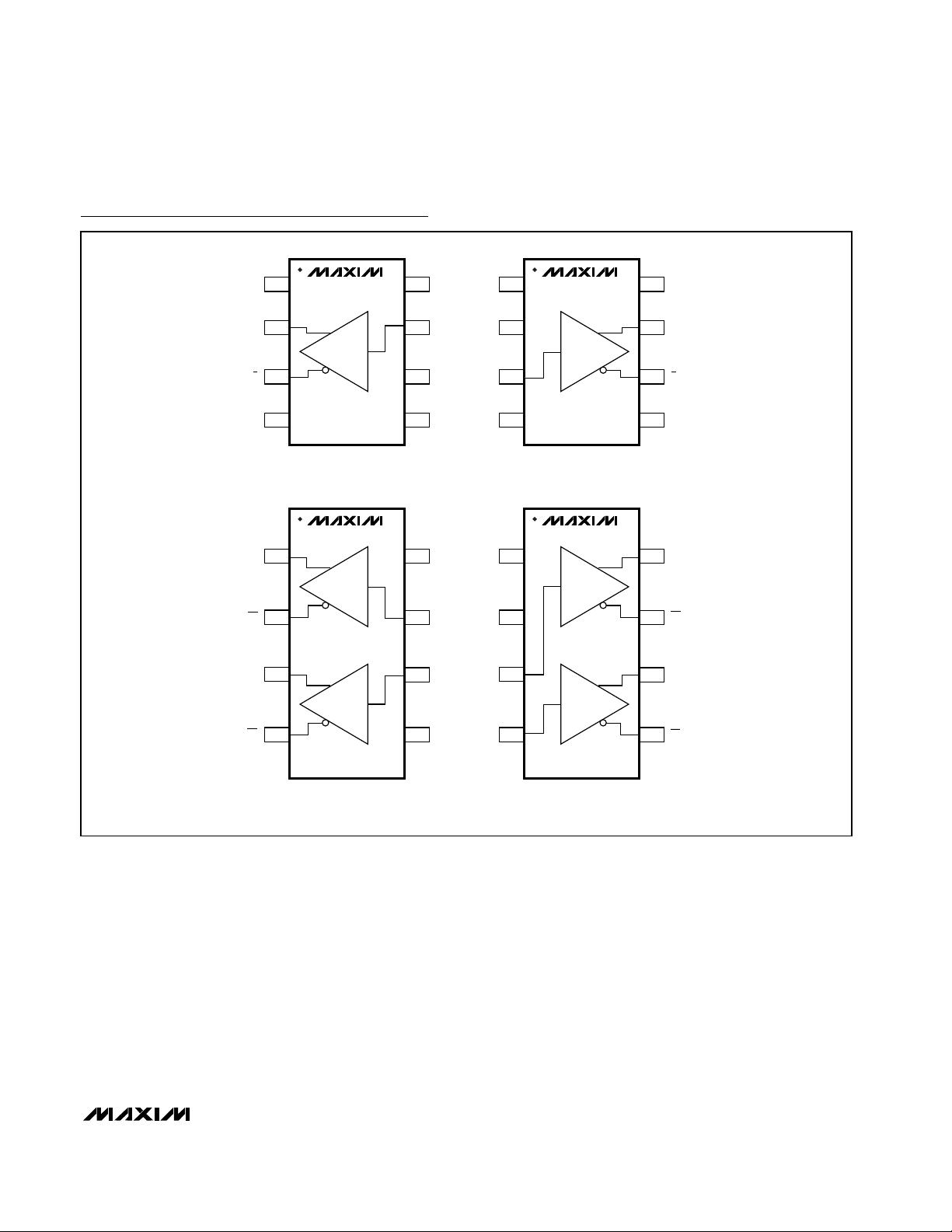
Pin Description for the MAX9370/MAX9372
PIN
SO
FUNCTION
1 8 Q0 Noninverting Differential LVPECL/PECL Output 0. Typically terminate with 50Ω resistor to V
CC
- 2V.
27Q0 Inverting Differential LVPECL/PECL Output 0. Typically terminate with 50Ω resistor to V
CC
- 2V.
3 6 Q1 Noninverting Differential LVPECL/PECL Output 1. Typically terminate with 50Ω resistor to V
CC
- 2V.
45Q1 Inverting Differential LVPECL/PECL Output 1. Typically terminate with 50Ω resistor to V
CC
- 2V.
52
Ground. Provide a low-impedance connection to ground plane.
6 4 D1 LVTTL/TTL Input 1. LVTTL/TTL input for translator corresponding to output Q1 and Q1.
7 3 D0 LVTTL/TTL Input 0. LVTTL/TTL input for translator corresponding to output Q0 and Q0.
81V
CC
Positive Supply Voltage. Bypass VCC to GND with 0.1µF and 0.01µF ceramic capacitors. Place the
capacitors as close to the device as possible with the smaller value capacitor closest to the device.
Pin Description for the MAX9371
PIN
SO
µMAX
FUNCTION
1, 4, 6
No Connection. No internal connection.
2 7 Q Noninverting Differential LVPECL/PECL Output. Typically terminate with 50Ω resistor to V
CC
- 2V.
36Q Inverting Differential LVPECL/PECL Output. Typically terminate with 50Ω resistor to V
CC
- 2V.
52
Ground. Provide a low-impedance connection to ground plane.
7 3 D LVTTL/TTL Input
81
Positive Supply Voltage. Bypass VCC to GND with 0.1µF and 0.01µF ceramic capacitors. Place the
capacitors as close to the device as possible with the smaller value capacitor closest to the device.
µMAX
SOT23
SOT23
4, 5, 8 N.C.
NAME
GND
NAME
GND
V
CC
Page 6

MAX9370/MAX9371/MAX9372
Ensure that the output currents do not exceed the continuous safe output current limit or surge output current
limit as specified in the Absolute Maximum Ratings
table. Under all operating conditions, the device’s total
thermal limits should be observed.
Supply Bypassing
Bypass VCCto GND with high-frequency surface-mount
ceramic 0.1µF and 0.01µF capacitors in parallel and as
close to the device as possible, with the 0.01µF capacitor closest to the device. Use multiple parallel vias to
minimize parasitic inductance.
PC Board Traces
Input and output trace characteristics affect the performance of the MAX9370/MAX9371/MAX9372. Connect
each differential output to a 50Ω characteristic impedance
trace. Minimize the number of vias to prevent impedance
discontinuities. Reduce reflections by maintaining the 50Ω
characteristic impedance through connectors and across
cables. Reduce skew within a differential pair by matching the electrical length of the traces.
Chip Information
TRANSISTOR COUNT: 358
PROCESS: Bipolar
LVTTL/TTL-to-Differential LVPECL/PECL
Translators
6 _______________________________________________________________________________________
D_
0V (DIFFERENTIAL)
20%
80%
20%
80%
t
R
t
F
Q_
Q_
Q_ - Q_
V
IH
V
IL
50%
t
PLH
50%
V
OH
V
OL
VOH - V
OL
VOH - V
OL
VOH - V
OL
t
PHL
Figure 1. Input-to-Output Propagation Delay and Transition Timing Diagram
Page 7
MAX9370/MAX9371/MAX9372
LVTTL/TTL-to-Differential LVPECL/PECL
Translators
_______________________________________________________________________________________ 7
1
N.C.
2
Q
3
4
N.C.
Q
8
V
CC
7
D
6
5
GND
N.C.
SO/µMAX
MAX9371
1
V
CC
2
GND
3
4
N.C.
D
8
N.C.
7
Q
6
5
N.C.
Q
SOT23
MAX9371
1
Q0
2
Q0
3
4
Q1
Q1
8
V
CC
7
D0
6
5
GND
D1
SO/µMAX
MAX9370/MAX9372
1
V
CC
2
GND
3
4
D1
D0
8
Q0
7
Q0
6
5
Q1
Q1
SOT23
MAX9370/MAX9372
Pin Configurations/Functional Diagrams
Page 8

MAX9370/MAX9371/MAX9372
LVTTL/TTL-to-Differential LVPECL/PECL
Translators
8 _______________________________________________________________________________________
Package Information
(The package drawing(s) in this data sheet may not reflect the most current specifications. For the latest package outline information,
go to www.maxim-ic.com/packages.)
SOT23, 8L.EPS
8LUMAXD.EPS
PACKAGE OUTLINE, 8L uMAX/uSOP
1
1
21-0036
J
REV.DOCUMENT CONTROL NO.APPROVAL
PROPRIETARY INFORMATION
TITLE:
MAX
0.043
0.006
0.014
0.120
0.120
0.198
0.026
0.007
0.037
0.0207 BSC
0.0256 BSC
A2
A1
c
e
b
A
L
FRONT VIEW
SIDE VIEW
E H
0.6±0.1
0.6±0.1
ÿ 0.50±0.1
1
TOP VIEW
D
8
A2
0.030
BOTTOM VIEW
1
6∞
S
b
L
H
E
D
e
c
0∞
0.010
0.116
0.116
0.188
0.016
0.005
8
4X S
INCHES
-
A1
A
MIN
0.002
0.950.75
0.5250 BSC
0.25 0.36
2.95 3.05
2.95 3.05
4.78
0.41
0.65 BSC
5.03
0.66
6∞0∞
0.13 0.18
MAX
MIN
MILLIMETERS
- 1.10
0.05 0.15
α
α
DIM
Page 9

MAX9370/MAX9371/MAX9372
LVTTL/TTL-to-Differential LVPECL/PECL
Translators
Maxim cannot assume responsibility for use of any circuitry other than circuitry entirely embodied in a Maxim product. No circuit patent licenses are
implied. Maxim reserves the right to change the circuitry and specifications without notice at any time.
Maxim Integrated Products, 120 San Gabriel Drive, Sunnyvale, CA 94086 408-737-7600 _____________________ 9
© 2002 Maxim Integrated Products Printed USA is a registered trademark of Maxim Integrated Products.
Package Information (continued)
(The package drawing(s) in this data sheet may not reflect the most current specifications. For the latest package outline information,
go to www.maxim-ic.com/packages.)
9LUCSP, 3x3.EPS
 Loading...