

General Description
The MAX9360/MAX9361 are low-skew, single LVTTL/
TTL/CMOS-to-differential LVECL/ECL translators
designed for high-speed signal and clock driver applications. For interfacing to LVTTL/TTL/CMOS input signals, these devices operate over a 3.0V to 5.5V supply
range, allowing high-performance clock or data distribution. For interfacing to differential LVECL/ECL output
signals, these devices operate from a -2.375V to -5.5V
supply.
The MAX9360 is a 3.3V LVTTL/CMOS-to-LVECL/ECL
translator that operates at a typical speed of 3GHz. The
MAX9361 is a 5V TTL/CMOS-to-LVECL/ECL translator
that operates at a typical speed of 1.3GHz. Both
devices can be used to drive either LVECL devices or
standard ECL devices with a negative supply range of
-2.375V to -5.5V.
The devices default to high if the input is disconnected,
and feature ultra-low propagation delay: 440ps for the
MAX9360, 810ps for the MAX9361.
The MAX9360 is specified for operation from -40°C to
+85°C in an 8-pin SO package, and 0°C to +85°C in a
space-saving, 8-pin SOT23 package.
The MAX9361 is specified for operation from -40°C to
+85°C for both 8-pin SO and SOT23 packages.
Applications
Clock/Data-Level Translation
Features
♦ Output High with Input Open
♦ -2.375V to -5.5V LVECL/ECL Operation
♦ ESD Protection >2kV (Human Body Model)
♦ 3.0V to 3.6V LVTTL/CMOS Operation (MAX9360)
Improved Second Source of the MC100EPT24
Low 13.8mA (typ) I
EE
Supply Current
440ps (typ) Propagation Delay
>300mV Output at 1GHz
♦ 4.5V to 5.5V TTL Operation (MAX9361)
Improved Second Source of the MC100ELT24
Low 6.6mA (typ) I
EE
Supply Current
600ps (typ) Propagation Delay
>300mV Output at 250MHz
MAX9360/MAX9361
LVTTL/TTL/CMOS-to-Differential LVECL/
ECL Translators
________________________________________________________________ Maxim Integrated Products 1
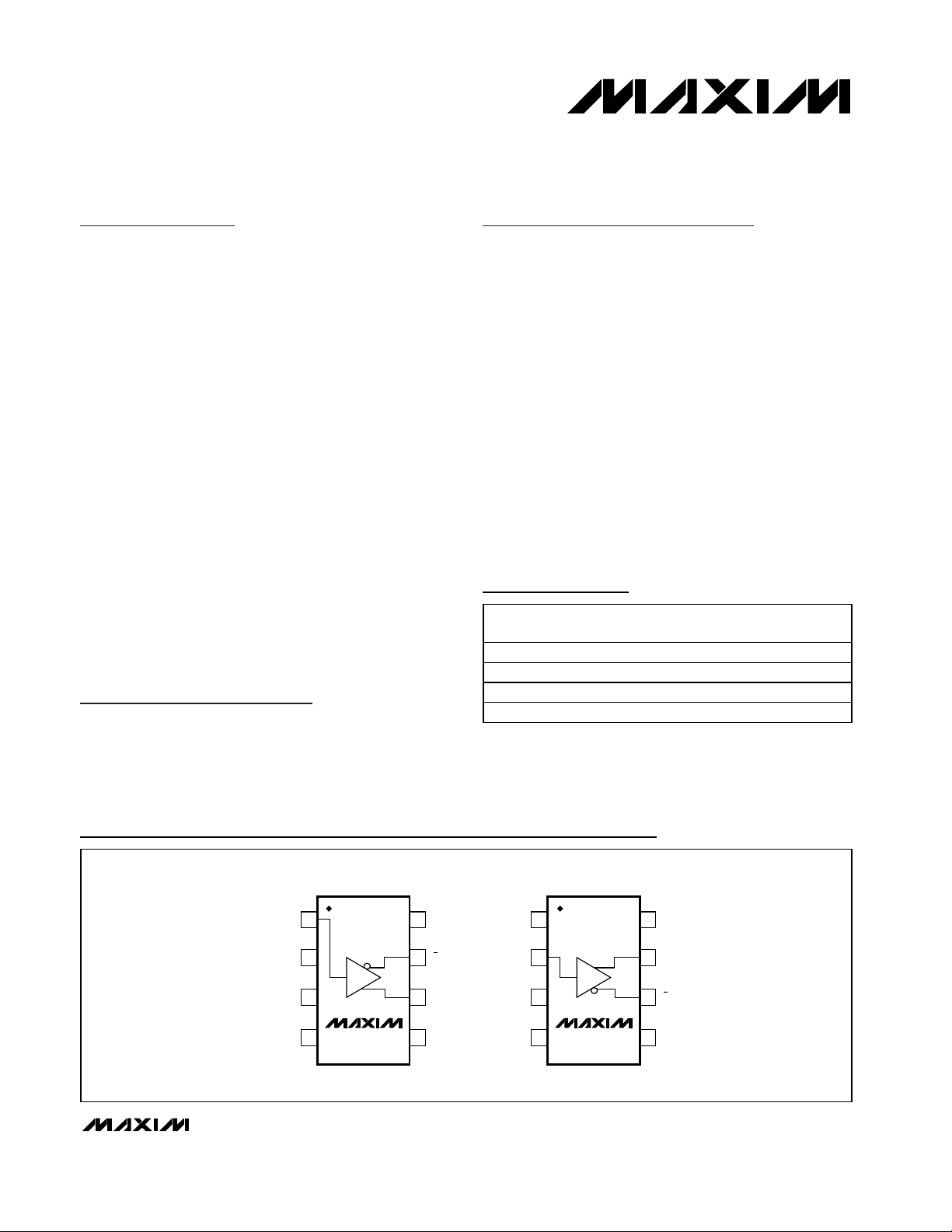
Ordering Information
TOP VIEW
GNDN.C.
1
2
87V
CC
QD
N.C.
V
EE
SO
3
4
6
5
MAX9360/
MAX9361
Q
GND
N.C.
1
2
8
7
V
CC
Q
V
EE
N.C.
D
SOT23
3
4
6
5
MAX9360/
MAX9361
Q
Pin Configurations
19-2327; Rev 1; 7/02
For pricing, delivery, and ordering information, please contact Maxim/Dallas Direct! at
1-888-629-4642, or visit Maxim’s website at www.maxim-ic.com.
PART TEMP RANGE
MAX9360EKA-T -40°C to +85°C 8 SOT23-8 AAJI
MAX9360ESA -40°C to +85°C 8 SO —
MAX9361EKA-T -40°C to +85°C 8 SOT23-8 AAJJ
MAX9361ESA -40°C to +85°C 8 SO —
PINPACKAGE
TOP
MARK
MAX9360/MAX9361
LVTTL/TTL/CMOS-to-Differential LVECL/
ECL Translators
2 _______________________________________________________________________________________
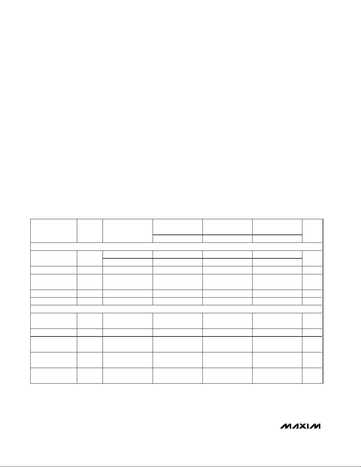
ABSOLUTE MAXIMUM RATINGS
DC ELECTRICAL CHARACTERISTICS—MAX9360
(VCC= 3.0V to 3.6V, VEE= -2.375V to -5.5V, GND = 0, outputs terminated with 50Ω ±1% to -2.0V. Typical values are at VCC= 3.3V,
V
IH
= 2.0V, VIL= 0.8V, unless otherwise noted.) (Notes 1, 2, 3)
Stresses beyond those listed under “Absolute Maximum Ratings” may cause permanent damage to the device. These are stress ratings only, and functional
operation of the device at these or any other conditions beyond those indicated in the operational sections of the specifications is not implied. Exposure to
absolute maximum rating conditions for extended periods may affect device reliability.
VCCto GND..............................................................-0.3V to +6V
VEEto GND...............................................................-6V to +0.3V
D to GND....................................................-0.3V to (VCC+ 0.3V)
Continuous Output Current ................................................50mA
Surge Output Current........................................................100mA
Junction-to-Ambient Thermal Resistance in Still Air
8-Pin SOT23.............................................................+112°C/W
8-Pin SO...................................................................+170°C/W
Junction-to-Ambient Thermal Resistance
with 500LFPM Airflow
8-Pin SOT23...............................................................+78°C/W
8-Pin SO.....................................................................+99°C/W
Junction-to-Case Thermal Resistance
8-Pin SOT23...............................................................+80°C/W
8-Pin SO..................................................................+40°C/mW
Continuous Power Dissipation (TA= +70°C)
8-Pin SOT23 (derate 8.9mW/°C above +70°C)............714mW
8-Pin SO (derate 5.9mW/°C above +70°C)..................470mW
Operating Temperature Range ...........................-40°C to +85°C
Junction Temperature......................................................+150°C
Storage Temperature Range .............................-60°C to +150°C
ESD Protection
Human Body Model (D, Q, Q).........................................>2kV
Soldering Temperature (10s) ...........................................+300°C
PARAMETER SYMBOL CONDITIONS
LVTTL INPUT (D)
Input High Current I
Input Low Current I
Input Clamp
Voltage
Input High Voltage V
Input Low Voltage V
LVECL/ECL OUTPUTS (Q, Q)
Output High
Voltage
Output Low Voltage V
Differential Output
Swing (V
Power-Supply
Current
Internal Chip
Current
OH
- VOL)
IH
IL
V
V
OH
OL
V
OH
V
OL
I
CC
I
EE
VIN = 2.7V -20 +20 -20 +20 -20 +20
VIN = V
CC
VIN = 0.5V -200 -51 -200 -60 -200 -67 µA
IIN = -18mA -1.2 -1.2 -1.2 V
IK
IH
IL
-
(Note 4) 4.3 7.0 5.0 7.0 5.6 7.0 mA
(Note 4) 12.3 20 13.8 20 15.2 20 mA
0°C (SOT23)
-40°C (SO)
MIN TYP MAX MIN TYP MAX MIN TYP MAX
-10 +10 -10 +10 -10 +10
2.0 2.0 2.0 V
-1.145 -0.885 -1.145 -0.885 -1.145 -0.885 V
-1.935 -1.625 -1.935 -1.625 -1.935 -1.625 V
550 550 550 mV
+25°C +85°C
0.8 0.8 0.8 V
UNITS
µA
MAX9360/MAX9361
LVTTL/TTL/CMOS-to-Differential LVECL/
ECL Translators
_______________________________________________________________________________________ 3
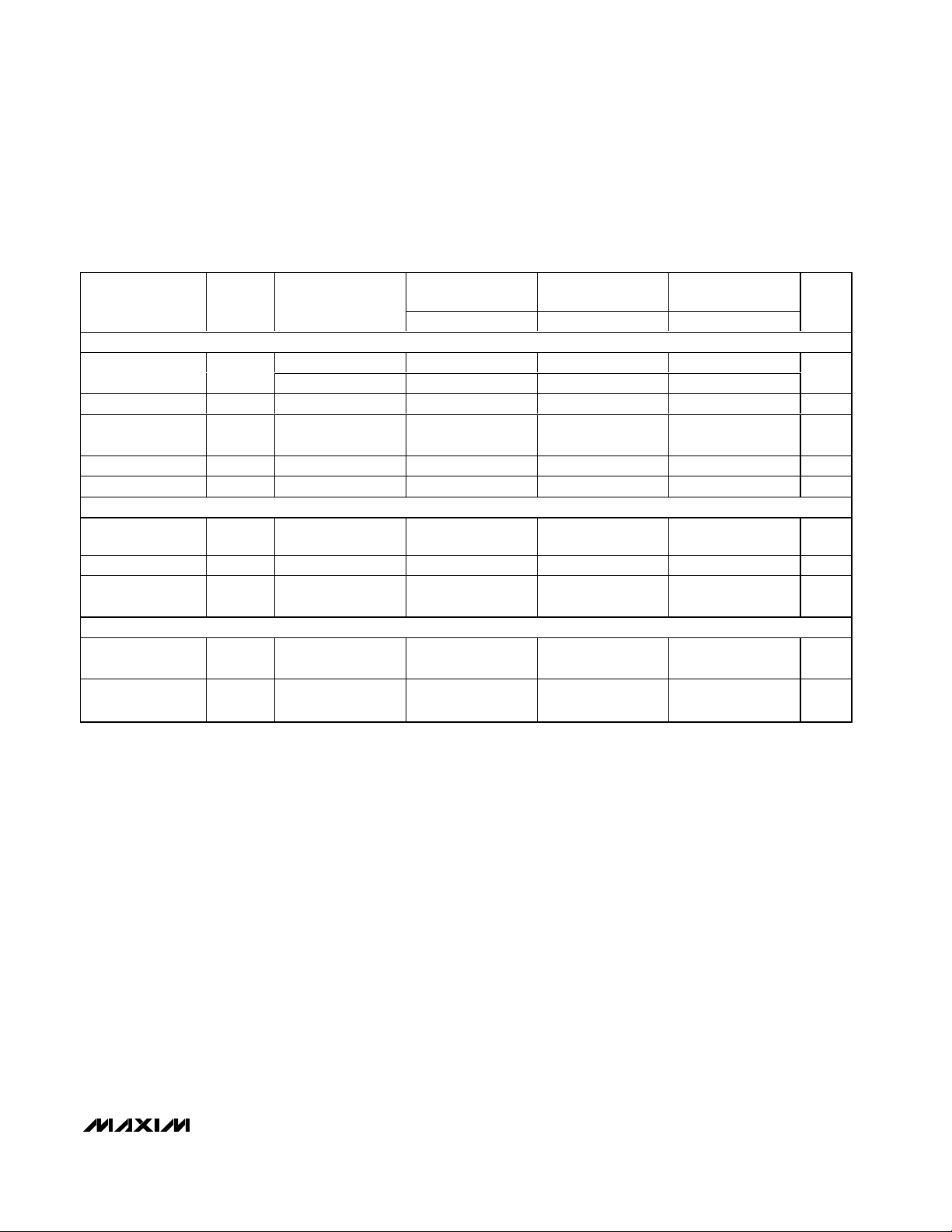
DC ELECTRICAL CHARACTERISTICS—MAX9361
(VCC= 4.5V to 5.5V, VEE= -2.375V to -5.5V, GND = 0, outputs terminated with 50Ω ±1% to -2.0V. Typical values are at VCC= 5V, V
IH
= 2.0V, VIL= 0.8V, unless otherwise noted.) (Notes 1, 2, 3)
PARAMETER SYMBOL CONDITIONS
TTL INPUT (D)
Input High Current I
Input Low Current I
Input Clamp
Voltage
Input High Voltage V
Input Low Voltage V
LVECL/ECL OUTPUTS (Q, Q)
Output High
Voltage
Output Low Voltage V
Differential Output
Swing (V
POWER SUPPLY
Power-Supply
Current
Internal Chip
Current
OH
- VOL)
IH
V
V
OH
OL
V
OH
V
OL
I
CC
I
EE
VIN = 2.7V -30 +30 -30 +30 -30 +30
VIN = V
CC
VIN = 0.5V -200 -55 -200 -61 -200 -71 µA
IL
IIN = -18mA -1.2 -1.2 -1.2 V
IK
IH
IL
-
(Note 4) 3.0 7.0 3.5 7.0 4.3 7.0 mA
(Note 4) 9 20 10 20 11 20 mA
-40°C (SO) +25°C +85°C
MIN TYP MAX MIN TYP MAX MIN TYP MAX
-10 +10 -10 +10 -10 +10
2.0 2.0 2.0 V
0.8 0.8 0.8 V
-1.055 -0.880 -1.055 -0.880 -1.025 -0.880 V
-1.875 -1.555 -1.810 -1.605 -1.810 -1.605 V
550 699 550 691 550 677 mV
UNITS
µA
Note 1: Measurements are made with the device in thermal equilibrium.
Note 2: Current into a pin is defined as positive. Current out of a pin is defined as negative.
Note 3: DC parameters are production tested at +25°C. DC limits are guaranteed by design and characterization over the full
operating temperature range.
Note 4: All pins are open except V
CC
, VEE, and GND.
Note 5: Guaranteed by design and characterization. Limits are set to ±6 sigma.
Note 6: Device jitter added to the input signal.
MAX9360/MAX9361
LVTTL/TTL/CMOS-to-Differential LVECL/
ECL Translators
4 _______________________________________________________________________________________
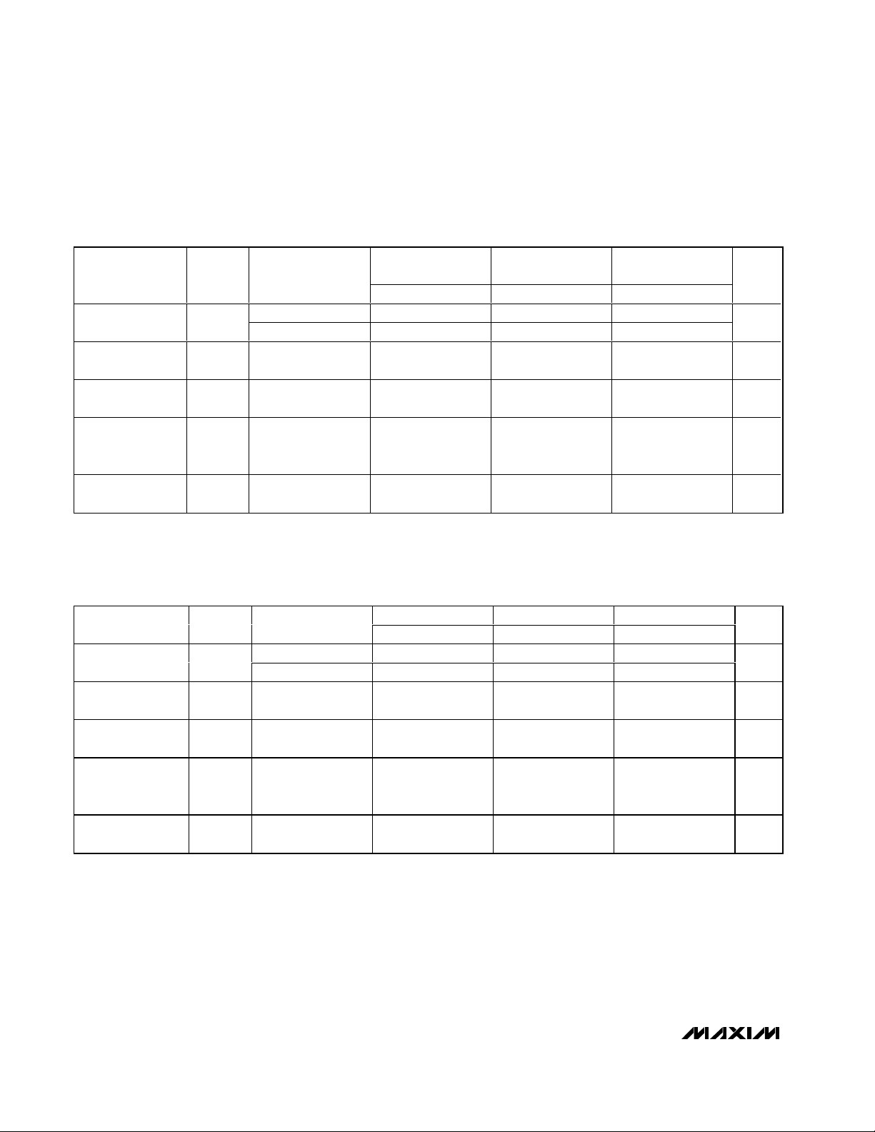
AC ELECTRICAL CHARACTERISTICS—MAX9360
(VCC= 3.0V to 3.6V, VEE= -2.375V to -5.5V, GND = 0, outputs terminated with 50Ω ±1% to -2.0V, input frequency = 1.0GHz, input
transition time = 125ps (20% to 80%). Typical values are at V
CC
= 3.3V, VIH= 2.0V, VIL= 0.8V, unless otherwise noted.) (Note 5)
(
)
(
)
AC ELECTRICAL CHARACTERISTICS—MAX9361
(VCC= 4.5V to 5.5V, VEE= -2.375V to -5.5V, GND = 0, outputs terminated with 50Ω ±1% to -2.0V, input frequency = 100MHz, input
transition time = 125ps (20% to 80%). Typical values are at V
CC
= 5.0V, VIH= 2.0V, VIL= 0.8V, unless otherwise noted.) (Note 5)
(
)
(
)
PARAMETER SYMBOL CONDITIONS
Maximum Toggle
Frequency
Input-to-Output
Propagation Delay
Output Rise/Fall
Time
Added
Deterministic Jitter
f
MAX
t
PLHD
t
PHLD
t
R
t
DJ
, t
VOH - VOL ≥ 300mV 1.0 3.0 1.0 3.0 1.0 3.0
VOH - VOL ≥ 500mV 0.85 1.5 0.85 1.5 0.85 1.5
,
Figure 1 300 800 300 800 300 800 ps
Figure 1 70 97 150 80 105 150 100 122 150 ps
F
2Gbps
23
2
- 1 PRBS pattern
(Note 6)
0°C (SOT23)
-40°C (SO)
+25°C +85°C
MIN TYP MAX MIN TYP MAX MIN TYP MAX
43 70 43 70 43 70 ps
UNITS
GHz
P-P
Added Random
Jitter
t
RJ
1.0GHz clock
pattern (Note 6)
1.4 3.0 1.5 3.0 1.5 3.0 ps
PARAMETER SYMBOL CONDITIONS
Maximum Toggle
Frequency
Input-to-Output
Propagation Delay
Output Rise/Fall
Time
Added
Deterministic Jitter
Added Random
Jitter
f
MAX
t
PLHD
t
PHLD
t
R
t
DJ
t
RJ
VOH - VOL ≥ 300mV 250 1300 250 1300 250 1300
VOH - VOL ≥ 500mV 150 500 150 500 150 500
,
Figure 1 300 561 900 300 583 900 300 607 900 ps
, t
Figure 1 250 340 1000 250 342 1000 250 353 1000 ps
F
200Mbps
23
- 1 PRBS pattern
2
(Note 6)
100MHz clock
pattern (Note 6)
-40°C +25° C +85°C
MIN TYP MAX MIN TYP MAX MIN TYP MAX
81 150 83 150 85 150 ps
410 410 410ps
RMS
UNITS
MHz
P-P
RMS

MAX9360/MAX9361
LVTTL/TTL/CMOS-to-Differential LVECL/
ECL Translators
_______________________________________________________________________________________ 5
Typical Operating Characteristics
(MAX9360: VCC= 3.3V and VEE= -5V, VIH= 2.0V, VIL= 0.8V, TA= +25°C, outputs terminated with 50Ω to -2V, input frequency
= 1GHz, input transition time = 125ps (20% to 80%), unless otherwise noted.)
SUPPLY CURRENT vs. TEMPERATURE
20
16
12
8
SUPPLY CURRENT (mA)
4
0
-40 10-15 35 60 85
I
EE
I
CC
TEMPERATURE (°C)
TRANSITION TIME vs. TEMPERATURE
130
120
110
100
TRANSITION TIME (ps)
90
t
R
t
F
MAX9360 toc01
MAX9360 toc03
OUTPUT AMPLITUDE vs. FREQUENCY
800
750
700
650
600
550
500
450
OUTPUT AMPLITUDE (mV)
400
350
300
0 1000500 1500 2000 2500 3000
FREQUENCY (MHz)
PROPAGATION DELAY vs. TEMPERATURE
500
475
450
425
400
PROPAGATION DELAY (ps)
375
t
PLHD
t
PHLD
MAX9360 toc02
MAX9360 toc4
80
-40 10-15 35 60 85
TEMPERATURE (°C)
350
-40 10-15 35 60 85
TEMPERATURE (°C)
MAX9360/MAX9361
LVTTL/TTL/CMOS-to-Differential LVECL/
ECL Translators
6 _______________________________________________________________________________________
Pin Description
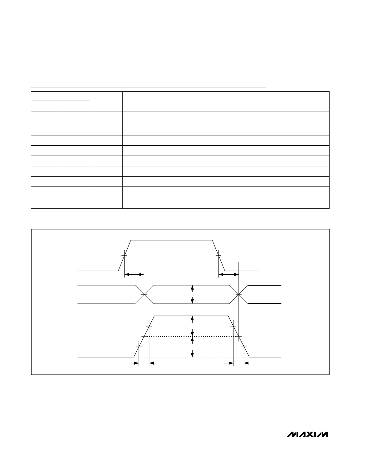
Figure 1. Input-to-Output Propagation Delay and Transition Timing Diagram
PIN
NAME FUNCTION
SO SOT23
Negative Supply Voltage. Bypass VEE to GND with 0.1µF and 0.01µF ceramic capacitors.
12V
EE
Place the capacitors as close to the device as possible with the smaller value capacitor
closest to the device.
2 1 D LVTTL/CMOS Input for MAX9360. TTL/CMOS input for MAX9361.
3, 4 3, 4 N.C. No Connect. Connect to GND.
5 8 GND Ground
67 Q Inverting Differential LVECL/ECL Output. Typically terminate with 50Ω resistor to -2V.
7 6 Q Noninverting Differential LVECL/ECL Output. Typically terminate with 50Ω resistor to -2V.
Positive Supply Voltage. Bypass VCC to GND with 0.1µF and 0.01µF ceramic capacitors.
85V
CC
Place the capacitors as close to the device as possible with the smaller value capacitor
closest to the device.
50% 50%
V
IH
D
Q
SINGLE-ENDED WAVEFORMS
Q
DIFFERENTIAL WAVEFORM
Q - Q
t
PLH
VOH - V
OL
80%
20% 20%
t
R
VOH - V
VOH - V
OL
OL
80%
t
PHL
0 (DIFFERENTIAL)
t
F
V
IL
V
OH
V
OL

Detailed Description
The MAX9360/MAX9361 are low-skew, single LVTTL/
CMOS/TTL-to-differential LVECL/ECL translators
designed for high-speed signal and clock driver applications. For interfacing to LVTTL/TTL/CMOS input signals, these devices operate over a 3.0V to 5.5V supply
range, allowing high-performance clock or data distribution in systems with a nominal 3.3V or 5.0V supply. For
interfacing to differential LVECL/ECL output signals,
these devices operate from a -2.375V to -5.5V supply.
The MAX9360 is a 3.3V LVTTL/CMOS-to-LVECL/ECL
translator that operates at typical speeds of 3GHz. The
MAX9361 is a 5V TTL/CMOS-to-LVECL/ECL translator that
operates at typical speeds of 1.3GHz. Both devices can
be used to drive either LVECL devices or standard ECL
devices with a negative supply range of -2.375V to -5.5V.
Input
The MAX9360/MAX9361 inputs accept standard LVTTL/
TTL/CMOS levels. The input has pullup circuitry that drives the outputs to a differential high if the inputs are open.
Differential Output
Output levels are referenced to GND and are considered
ECL or LVECL, depending on the level of the VEEsupply.
With GND connected to zero and VEEat -4.2V to -5.5V,
the outputs are ECL. The outputs are LVECL when GND is
connected to zero and VEEis at -2.375V to -3.8V.
Applications Information
Supply Bypassing
Bypass VCCand VEEto ground with high-frequency
surface-mount ceramic 0.1µF and 0.01µF capacitors in
parallel as close to the device as possible, with the
0.01µF value capacitor closest to the device. Use multiple parallel vias for low inductance.
Traces
Input and output trace characteristics affect the performance of the MAX9360/MAX9361. Connect each signal
of a differential output to a 50Ω characteristic impedance trace. Minimize the number of vias to prevent
impedance discontinuities. Reduce reflections by maintaining the 50Ω characteristic impedance through connectors and across cables. Reduce skew within a
differential pair by matching the electrical length of the
traces.
On the MAX9360, if the input edge rate approaches the
electrical length of the interconnect, then controlledimpedance transmission lines should be used for the
input traces.
Output Termination
Terminate outputs through 50Ω to -2V or use an equivalent Thevenin termination. Terminate both outputs and
use the same termination on each for the lowest outputto-output skew. When a single-ended signal is taken
from a differential output, terminate both outputs. For
example, if Q is used as a single-ended output, terminate both Q and Q.
Ensure that the output currents do not exceed the continuous safe output current limit or surge output current
limit as specified in the Absolute Maximum Ratings
table. Under all operating conditions, the device’s total
thermal limits should be observed.
Chip Information
TRANSISTOR COUNT: 330
PROCESS: Bipolar
MAX9360/MAX9361
LVTTL/TTL/CMOS-to-Differential LVECL/
ECL Translators
_______________________________________________________________________________________ 7

MAX9360/MAX9361
LVTTL/TTL/CMOS-to-Differential LVECL/
ECL Translators
8 _______________________________________________________________________________________
Package Information
(The package drawing(s) in this data sheet may not reflect the most current specifications. For the latest package outline information,
go to www.maxim-ic.com/packages.)
SOT23, 8L.EPS

MAX9360/MAX9361
LVTTL/TTL/CMOS-to-Differential LVECL/
ECL Translators
Maxim cannot assume responsibility for use of any circuitry other than circuitry entirely embodied in a Maxim product. No circuit patent licenses are
implied. Maxim reserves the right to change the circuitry and specifications without notice at any time.
Maxim Integrated Products, 120 San Gabriel Drive, Sunnyvale, CA 94086 408-737-7600 _____________________ 9
© 2002 Maxim Integrated Products Printed USA is a registered trademark of Maxim Integrated Products.
Package Information (continued)
(The package drawing(s) in this data sheet may not reflect the most current specifications. For the latest package outline information,
go to www.maxim-ic.com/packages.)
SOICN.EPS

 Loading...