

Page 1
General Description
The MAX9323 low-skew, low-jitter, clock and data driver distributes one of two single-ended LVCMOS inputs
to four differential LVPECL outputs. A single logic control signal (CLK_SEL) selects the input signal to distribute to all outputs. The device operates from 3.0V to
3.6V, making the device ideal for 3.3V systems, and
consumes only 25mA (max) of supply current.
The MAX9323 features low 150ps part-to-part skew, low
11ps output-to-output skew, and low 1.7ps RMS jitter,
making the device ideal for clock and data distribution
across a backplane or board. All outputs are enabled
and disabled synchronously with the clock input to prevent partial output clock pulses.
The MAX9323 is available in space-saving 20-pin
TSSOP and ultra-small 20-pin 4mm ✕ 4mm thin QFN
packages and operates over the extended (-40°C to
+85°C) temperature range. The MAX9323 is pin compatible with Integrated Circuit Systems’ ICS8535-01.
Applications
Precision Clock Distribution
Low-Jitter Data Repeater
Data and Clock Driver and Buffer
Central-Office Backplane Clock Distribution
DSLAM Backplane
Base Station
Hubs
Features
♦ 1.7ps
RMS
Added Random Jitter
♦ 150ps (max) Part-to-Part Skew
♦ 11ps Output-to-Output Skew
♦ 450ps Propagation Delay
♦ Pin Compatible with ICS8535-01
♦ Consumes Only 25mA (max) Supply Current
(50% Less than ICS8535-01)
♦ Synchronous Output Enable/Disable
♦ Two Selectable LVCMOS Inputs
♦ 3.0V to 3.6V Supply Voltage Range
♦ -40°C to +85°C Operating Temperature Range
MAX9323
One-to-Four LVCMOS-to-LVPECL
Output Clock and Data Driver
________________________________________________________________ Maxim Integrated Products 1
Ordering Information
19-2575; Rev 0; 10/02
For pricing, delivery, and ordering information, please contact Maxim/Dallas Direct! at
1-888-629-4642, or visit Maxim’s website at www.maxim-ic.com.
Functional Diagram and Typical Operating Circuit appear at
end of data sheet.
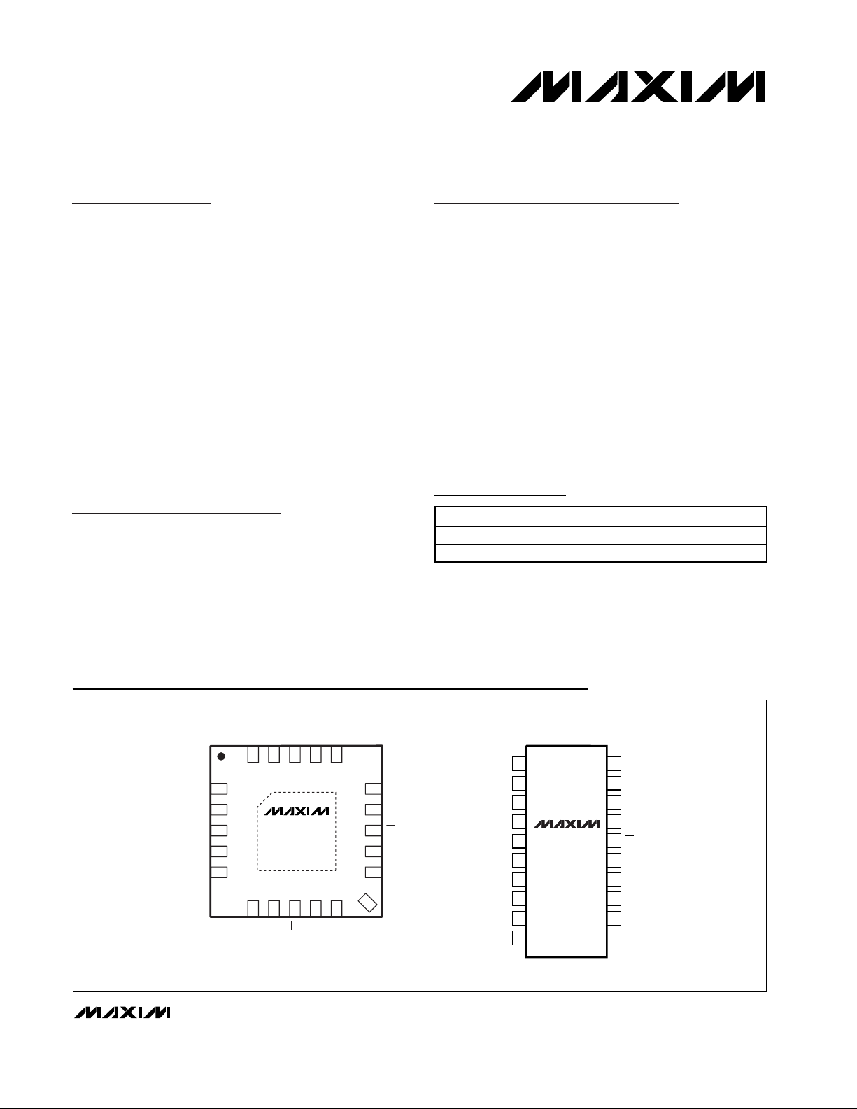
Pin Configurations
*Future product—Contact factory for availability.
**EP = Exposed paddle.
MAX9323EUP -40°C to +85°C 20 TSSOP
MAX9323ETP* -40°C to +85°C 20 Thin QFN-EP**
PART TEMP RANGE PIN-PACKAGE
CLK_SEL
CLK_EN
TOP VIEW
1
CLK0
2
N.C.
3
CLK1
4
N.C.
5
N.C.
678910
THIN QFN-EP** (4mm x 4mm)
**CONNECT EXPOSED PADDLE TO GND.
GNDQ0Q0
MAX9323
**EXPOSED PADDLE
CC
Q3
V
N.C.
1617181920
V
15
CC
Q1
14
Q1
13
12
Q2
11
Q2
CC
Q3
V
GND
CLK_EN
CLK_SEL
N.C.
CLK1
N.C.
N.C.
N.C.
V
1
2
3
4
MAX9323
5
6
7
8
9
10
CC
TSSOP
20
Q0
19
Q0
18
V
CC
17
Q1CLK0
Q1
16
15
Q2
14
Q2
13
V
CC
12
Q3
Q3
11
Page 2
MAX9323
One-to-Four LVCMOS-to-LVPECL
Output Clock and Data Driver
2 _______________________________________________________________________________________
ABSOLUTE MAXIMUM RATINGS
DC ELECTRICAL CHARACTERISTICS
(VCC= 3.0V to 3.6V, outputs terminated with 50Ω ±1% to (VCC- 2V), CLK_SEL = VCCor GND, CLK_EN = VCC, TA= -40°C to +85°C,
unless otherwise noted. Typical values are at V
CC
= 3.3V, TA= +25°C.) (Notes 1, 2, and 3)
Stresses beyond those listed under “Absolute Maximum Ratings” may cause permanent damage to the device. These are stress ratings only, and functional
operation of the device at these or any other conditions beyond those indicated in the operational sections of the specifications is not implied. Exposure to
absolute maximum rating conditions for extended periods may affect device reliability.
VCCto GND...........................................................-0.3V to +4.0V
Q_, Q_, CLK_, CLK_SEL,
CLK_EN to GND.....................................-0.3V to (V
CC
+ 0.3V)
Continuous Output Current .................................................50mA
Surge Output Current........................................................100mA
Continuous Power Dissipation (T
A
= +70°C)
20-Pin TSSOP (derate 11mW/°C)..............................879.1mW
20-Pin 4mm
✕ 4mm Thin QFN (derate 16.9mW/°C)...1349.1mW
Junction-to-Ambient Thermal Resistance in Still Air
20-Pin TSSOP ............................................................+91°C/W
20-Pin 4mm
✕ 4mm Thin QFN.................................+59.3°C/W
Junction-to-Case Thermal Resistance
20-Pin TSSOP ............................................................+20°C/W
20-Pin 4mm
✕ 4mm Thin QFN......................................+2°C/W
Operating Temperature Range ...........................-40°C to +85°C
Junction Temperature......................................................+150°C
Storage Temperature Range .............................-65°C to +150°C
Soldering Temperature (10s) ...........................................+300°C
INPUTS (CLK0, CLK1, CLK_SEL, CLK_EN)
Input High Voltage V
Input Low Voltage V
Input High Current I
Input Low Current I
Input Capacitance C
OUTPUTS (Q_, Q_)
Single-Ended Output High
Voltage
Single-Ended Output Low
Voltage
Differential Output Voltage V
SUPPLY
Supply Current (Note 5) I
PARAMETER SYM B O L CONDITIONS MIN TYP MAX UNITS
IH
IL
IH
IL
IN
V
OH
V
OL
OD
CC
Figure 1
Figure 1
CLK0, CLK1, CLK_SEL = V
CLK_EN = V
CLK0, CLK1, CLK_SEL = GND -5 +5
CLK_EN = GND -150
CLK0, CLK1, CLK_SEL, CLK_EN (Note 4) 4 pF
Figure 1
Figure 1
Figure 1, VOD = VOH - V
CLK0, CLK1 2 V
CLK_EN, CLK_SEL 2 V
CLK0, CLK1 0 1.3
CLK_EN, CLK_SEL 0 0.8
CC
OL
CC
-5 +5
V
-
CC
1.4
V
-
CC
2.0
0.6 0.85 V
VCC -
VCC -
CC
CC
150
1.0
1.7
25 mA
V
V
µA
µA
V
V
Page 3
MAX9323
One-to-Four LVCMOS-to-LVPECL
Output Clock and Data Driver
_______________________________________________________________________________________ 3
Note 1: Measurements are made with the device in thermal equilibrium.
Note 2: Positive current flows into a pin. Negative current flows out of a pin.
Note 3: DC parameters are production tested at T
A
= +25°C and guaranteed by design over the full operating temperature range.
Note 4: Guaranteed by design and characterization. Limits are set at ±6 sigma.
Note 5: All pins open except V
CC
and GND.
Note 6: Measured from the 50% point of the input to the crossing point of the differential output signal.
Note 7: Measured between outputs of the same part at the differential signal crosspoint for a same-edge transition.
Note 8: Measured between outputs of different parts at the differential signal crosspoint under identical conditions for a same-edge
transition.
Note 9: Jitter added to the input signal.
AC ELECTRICAL CHARACTERISTICS
(VCC= 3.0V to 3.6V, outputs terminated with 50Ω ±1% to (VCC-2V), fIN< 266MHz, input duty cycle = 50%, input transition time =
1.1ns (20% to 80%), V
IH
= VCC, VIL= GND, CLK_SEL = VCCor GND, CLK_EN = VCC, TA= -40°C to +85°C, unless otherwise noted.
Typical values are at V
CC
= 3.3V, TA= +25°C.) (Note 4)
(
)
(
)
Switching Frequency f
Propagation Delay t
Output-to-Output Skew t
Part-to-Part Skew t
Output Rise Time t
Output Fall Time t
Output Duty Cycle ODC 48 50 52 %
Added Random Jitter t
Added Jitter (Note 9) t
PARAMETER SYM B O L CONDITIONS MIN TYP MAX UNITS
PHL
MAX
, t
SKOO
SKPP
R
F
RJ
AJ
VOH - VOL ≥ 0.6V 266 800
VOH - VOL ≥ 0.3V 1500
CLK0 or CLK1 to Q_, Q_, Figure 1 (Note 6) 100 450 600 ps
PLH
(Note 7) 30 ps
(Note 8) 150 ps
20% to 80%, Figure 1 100 203 300 ps
80% to 20%, Figure 1 100 198 300 ps
fIN = 266MHz, clock pattern (Note 9) 1.7 3 ps
VCC = 3.3V with 25mV superimposed
sinusoidal noise at 100kHz
10 ps
MHz
RMS
P-P
Page 4
MAX9323
One-to-Four LVCMOS-to-LVPECL
Output Clock and Data Driver
4 _______________________________________________________________________________________
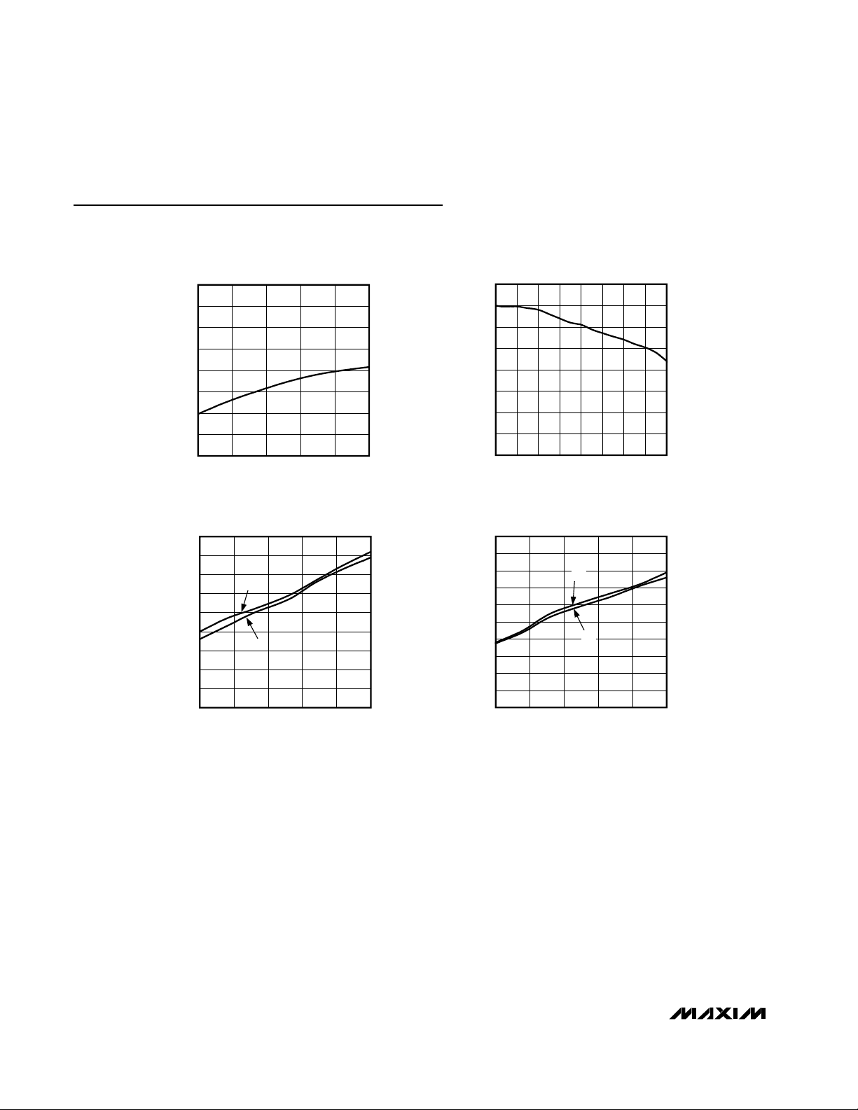
Typical Operating Characteristics
(VCC= 3.3V, outputs terminated to (VCC- 2V) through 50Ω, CLK_SEL = VCCor GND, CLK_EN = VCC, TA= +25°C.)
SUPPLY CURRENT vs. TEMPERATURE
MAX9323 toc01
TEMPERATURE (°C)
SUPPLY CURRENT (mA)
6035-15 10
10.5
11.0
11.5
12.0
12.5
13.0
13.5
14.0
10.0
-40 85
OUTPUT AMPLITUDE (VOH - VOL)
vs. FREQUENCY
MAX9323 toc02
FREQUENCY (MHz)
OUTPUT AMPLITUDE (mV)
14001200200 400 600 800 1000
100
200
300
400
500
600
700
800
0
0 1600
OUTPUT RISE/FALL TIME
vs. TEMPERATURE
MAX9323 toc03
TEMPERATURE (°C)
OUTPUT RISE/FALL TIME (ps)
603510-15
150
160
170
180
190
200
210
220
230
140
-40 85
t
F
t
R
PROPAGATION DELAY
vs. TEMPERATURE
MAX9323 toc04
TEMPERATURE (°C)
PROPAGATION DELAY (ps)
603510-15
410
420
430
440
450
460
470
480
490
500
400
-40 85
t
PHL
t
PLH
Page 5

Detailed Description
The MAX9323 low-skew, low-jitter, clock and data driver distributes one of two single-ended LVCMOS input
signals to four differential LVPECL outputs. An input
multiplexer allows selection of one of the two input signals. The output drivers operate at frequencies up to
1.5GHz. The MAX9323 operates from 3.0V to 3.6V,
making it ideal for 3.3V systems.
Data Inputs
Single-Ended LVCMOS Inputs
The MAX9323 accepts two single-ended LVCMOS
inputs (CLK0 and CLK1, Figure 1). An internal reference (VCC/2) provides the input thresold voltage for
CLK0 and CLK1. CLK_SEL selects the CLK0 input or
CLK1 input to be converted to four differential LVPECL
signals (see Table 1). Connect CLK_SEL to GND to
select CLK0. Connect CLK_SEL to V
CC
to select CLK1.
CLK0 and CLK1 are pulled to GND through internal
51kΩ resistors, when not connected.
CLK_EN Input
CLK_EN enables/disables the differential outputs of the
MAX9323. Connect CLK_EN to VCCto enable the differential outputs. The (Q_, Q_) outputs are driven to a differential low condition when CLK_EN = GND. Each
differential output pair disables following successive rising and falling edges on CLK_, after CLK_EN connects to
GND. Both a rising and falling edge on CLK_ are required
to complete the enable/disable function (Figure 2).
CLK_SEL Input
CLK_SEL selects which single-ended LVCMOS input
signal is output differentially as four LVPECL signals.
Connect CLK_SEL to GND to select the CLK0 input.
MAX9323
One-to-Four LVCMOS-to-LVPECL
Output Clock and Data Driver
_______________________________________________________________________________________ 5
Pin Description
PIN
TSSOP QFN
1 18 GND Ground. Provide a low-impedance connection to the ground plane.
2 19 CLK_EN
3 20 CLK_SEL
4 1 CLK0
5, 7, 8, 9 2, 4, 5, 6 N.C. No Connect. Not internally connected.
6 3 CLK1
10, 13, 18 7, 10, 15 V
11 8 Q3 Inverting Differential LVPECL Output. Terminate Q3 to (VCC - 2V) with a 50Ω ±1% resistor.
12 9 Q3 Noninverting Differential LVPECL Output. Terminate Q3 to (VCC - 2V) with a 50Ω ±1% resistor.
14 11 Q2 Inverting Differential LVPECL Output. Terminate Q2 to (VCC - 2V) with a 50Ω ±1% resistor.
15 12 Q2 Noninverting Differential LVPECL Output. Terminate Q2 to (VCC - 2V) with a 50Ω ±1% resistor.
16 13 Q1 Inverting Differential LVPECL Output. Terminate Q1 to (VCC - 2V) with a 50Ω ±1% resistor.
17 14 Q1 Noninverting Differential LVPECL Output. Terminate Q1 to (VCC - 2V) with a 50Ω ±1% resistor.
19 16 Q0 Inverting Differential LVPECL Output. Terminate Q0 to (VCC - 2V) with a 50Ω ±1% resistor.
20 17 Q0 Noninverting Differential LVPECL Output. Terminate Q0 to (VCC - 2V) with a 50Ω ±1% resistor.
NAME FUNCTION
Synchronous Output Enable. Connect CLK_EN to V
differential outputs. Connect CLK_EN to GND to disable the differential outputs. When
disabled, Q_ asserts low and Q_ asserts high. An internal 51kΩ pullup resistor to V
CLK_EN to be left floating.
Clock Select Input. Connect CLK_SEL to V
GND or leave floating to select the CLK0 input. Only the selected CLK_ signal is reproduced
at each output. An internal 51kΩ pulldown resistor to GND allows CLK_SEL to be left floating.
LVCMOS Clock Input. When CLK_SEL = GND, each set of outputs differentially reproduces
CLK0. An internal 51kΩ pulldown resistor to GND forces the outputs (Q_, Q_) to differential low
when CLK0 is left open or at GND, CLK_SEL = GND, and the outputs are enabled.
LVCMOS Clock Input. When CLK_SEL = V
CLK1. An internal 51kΩ pulldown resistor to GND forces the outputs (Q_, Q_) to differential low
when CLK1 is left open or at GND, CLK_SEL = V
Positive Supply Voltage. Bypass VCC to GND with three 0.01µF and one 0.1µF ceramic
capacitors. Place the 0.01µF capacitors as close to each V
CC
input). Connect all VCC inputs together, and bypass to GND with a 0.1µF ceramic capacitor.
to select the CLK1 input. Connect CLK_SEL to
CC
, each set of outputs differentially reproduces
CC
CC
or leave floating to enable the
CC
, and the outputs are enabled.
CC
CC
input as possible (one per V
allows
CC
Page 6

MAX9323
One-to-Four LVCMOS-to-LVPECL
Output Clock and Data Driver
6 _______________________________________________________________________________________
Figure 1. MAX9323 Clock Input-to-Output Delay and Rise/Fall Time
Figure 2. MAX9323 CLK_EN Timing Diagram
V
CLK0/CLK1
50% OF CLK INPUT
V
IL
IH
Q_ - Q_
Q_
V
OH
V
OL
Q_
t
PLH
DIFFERENTIAL
OUTPUT
WAVEFORM
20%
CLK0 OR
CLK1
V
OD
80% 80%
t
R
t
F
t
PHL
0V
(DIFFERENTIAL)
20%
DISABLED
CLK_EN
Q_
Q_
ENABLED
Page 7

Connect CLK_SEL to VCCto select the CLK1 input. An
internal 51kΩ pulldown resistor to GND allows
CLK_SEL to be left floating.
Applications Information
Output Termination
Terminate both outputs of each differential pair through
50Ω to (V
CC
- 2V) or use an equivalent Thevenin termination. Use identical termination on each output for the
lowest output-to-output skew. Terminate both outputs
when deriving a single-ended signal from a differential
output. For example, using Q0 as a single-ended output requires termination for both Q0 and Q0.
Ensure that the output currents do not violate the current limits as specified in the Absolute Maximum
Ratings table. Observe the device’s total thermal limits
under all operating conditions.
Power-Supply Bypassing
Bypass VCCto GND using three 0.01µF ceramic
capacitors and one 0.1µF ceramic capacitor. Place the
0.01µF capacitors (one per VCCinput) as close to V
CC
as possible (see the Typical Operating Circuit). Use
multiple bypass vias to minimize parasitic inductance.
Circuit Board Traces
Input and output trace characteristics affect the performance of the MAX9323. Connect each input and output
to a 50Ω characteristic impedance trace to minimize
reflections. Avoid discontinuities in differential imped-
ance and maximize common-mode noise immunity by
maintaining the distance between differential traces
and avoiding sharp corners. Minimize the number of
vias to prevent impedance discontinuities. Minimize
skew by matching the electrical length of the traces.
Chip Information
TRANSISTOR COUNT: 4430
PROCESS: BiCMOS
MAX9323
One-to-Four LVCMOS-to-LVPECL
Output Clock and Data Driver
_______________________________________________________________________________________ 7
Table 1. Control Input Table
Functional Diagram
CLK_EN CLK_SEL SELECTED SOURCE Q0–Q3 Q0–Q3
0 0 CLK0 Disabled, pulled to logic low Disabled, pulled to logic high
0 1 CLK1 Disabled, pulled to logic low Disabled, pulled to logic high
1 0 CLK0 Enabled Enabled
1 1 CLK1 Enabled Enabled
INPUTS OUTPUTS
V
V
CC
CC
CLK_EN
51kΩ
V
CC
MAX9323
D
Q
CLK
CLK0
51kΩ
CLK1
51kΩ
0
GND
1
V
CC
Q0
Q0
Q1
Q1
Q2
Q2
GND
CLK_SEL
51kΩ
GND
GND
Q3
Q3
Page 8

MAX9323
One-to-Four LVCMOS-to-LVPECL
Output Clock and Data Driver
8 _______________________________________________________________________________________
Typical Operating Circuit
3.0V TO
3.6V
0.01µF 0.01µF 0.01µF
0.1µF
ON
OFF
CLK_SEL
CLK0
CLK1
CLK_EN
V
CC
V
CC
MAX9323
GND
V
CC
Q0
Q0
Q1
Q1
Q2
Q2
Q3
Q3
ZO = 50Ω
ZO = 50Ω
ZO = 50Ω
ZO = 50Ω
ZO = 50Ω
ZO = 50Ω
ZO = 50Ω
ZO = 50Ω
50Ω 50Ω
VCC - 2V
LVPECL
RECEIVER
Page 9

MAX9323
One-to-Four LVCMOS-to-LVPECL
Output Clock and Data Driver
_______________________________________________________________________________________ 9
Package Information
(The package drawing(s) in this data sheet may not reflect the most current specifications. For the latest package outline information,
go to www.maxim-ic.com/packages.)
PACKAGE OUTLINE
12,16,20,24L QFN THIN, 4x4x0.8 mm
21-0139 A
Page 10

MAX9323
One-to-Four LVCMOS-to-LVPECL Output Clock
and Data Driver
10 ______________________________________________________________________________________
Package Information (continued)
(The package drawing(s) in this data sheet may not reflect the most current specifications. For the latest package outline information,
go to www.maxim-ic.com/packages.)
PACKAGE OUTLINE
12,16,20,24L QFN THIN, 4x4x0.8 mm
A21-0139
Page 11

MAX9323
One-to-Four LVCMOS-to-LVPECL Output Clock
and Data Driver
Maxim cannot assume responsibility for use of any circuitry other than circuitry entirely embodied in a Maxim product. No circuit patent licenses are
implied. Maxim reserves the right to change the circuitry and specifications without notice at any time.
Maxim Integrated Products, 120 San Gabriel Drive, Sunnyvale, CA 94086 408-737-7600 ____________________ 11
© 2002 Maxim Integrated Products Printed USA is a registered trademark of Maxim Integrated Products.
Package Information (continued)
(The package drawing(s) in this data sheet may not reflect the most current specifications. For the latest package outline information,
go to www.maxim-ic.com/packages.)
TSSOP4.40mm.EPS
 Loading...