

Page 1
General Description
The MAX9322 low-skew 1:15 differential clock driver
reproduces or divides one of two differential input clocks
at 15 differential outputs. An input multiplexer selects from
one of two input clocks with input switching frequency in
excess of 1.0GHz. The 15 outputs are arranged in four
banks with 2, 3, 4, and 6 outputs, respectively. Each
output bank is individually programmable to provide a
divide-by-1 or divide-by-2 frequency function.
The MAX9322 operates in LVPECL systems with a
+2.375V to +3.8V supply or in LVECL systems with a
-2.375V to -3.8V supply. A VBBreference output provides compatibility with single-ended clock input signals and a master reset input provides a simultaneous
reset on all outputs.
The MAX9322 is available in 52-pin TQFP and 68-pin
QFN packages and is specified for operation over
-40°C to +85°C. For 1:10 clock drivers, refer to the
MAX9311/MAX9313 data sheet. For 1:5 clock drivers,
refer to the MAX9316 data sheet.
Applications
Precision Clock Distribution
Low-Jitter Data Repeaters
Central-Office Backplane Clock Distribution
DSLAM Backplane
Base Stations
ATE
Features
♦ 1.2ps (RMS) Maximum Random Jitter
♦ 300mV Differential Output at 1.0GHz
♦ 900ps Propagation Delay
♦ Selectable Divide-by-1 or Divide-by-2 Frequency
Outputs
♦ Multiplexed 2:1 Input Function
♦ LVECL Operation from V
EE
= -2.375V to -3.8V
♦ LVPECL Operation from V
CC
= +2.375V to +3.8V
♦ ESD Protection: > 2kV Human Body Model
MAX9322
LVECL/LVPECL 1:15 Differential
Divide-by-1/Divide-by-2 Clock Driver
________________________________________________________________ Maxim Integrated Products 1
32
TQFP
TOP VIEW
27
52
VCCO51QA050QA049QA148QA147VCCO46QB045QB044QB143QB142QB241QB2
40
VCCO
VCCO
14
QD515QD5
16
QD417QD418QD319QD320QD221QD1
23
QD222QD124QD0
26
QD0
25
VCCO
28 N.C.
29 N.C.
30 VCCO
31 QC3
QC3
34 QC2
33 QC2
35 QC1
36 QC1
37 QC0
38 QC0
39 VCCO
FSELD 12
V
EE
13
FSELC 11
V
BB
10
CLK1 9
CLK1 8
CLK_SEL 7
CLK0 6
CLK0 5
FSELA
3
FSELB 4
MR
2
V
CC
1
MAX9322
Pin Configurations
Ordering Information
Typical Operating Circuit
19-2544; Rev 2; 2/07
For pricing, delivery, and ordering information, please contact Maxim/Dallas Direct! at
1-888-629-4642, or visit Maxim’s website at www.maxim-ic.com.
PART
TEMP RANGE
PINPACKAGE
MAX9322ECY -40°C to +85°C 52 TQFP
MAX9322ETK* -40°C to +85°C 68 QFN
*Future product—contact factory for availability.
50Ω 50Ω
MAX9322
ZO = 50Ω
Z
O
= 50Ω
RECEIVER
Q_
Q_
VTT = VCC - 2.0V
Pin Configurations continued at end of data sheet.
Page 2
MAX9322
LVECL/LVPECL 1:15 Differential
Divide-by-1/Divide-by-2 Clock Driver
2 _______________________________________________________________________________________
ABSOLUTE MAXIMUM RATINGS
Stresses beyond those listed under “Absolute Maximum Ratings” may cause permanent damage to the device. These are stress ratings only, and functional
operation of the device at these or any other conditions beyond those indicated in the operational sections of the specifications is not implied. Exposure to
absolute maximum rating conditions for extended periods may affect device reliability.
VCCto VEE.............................................................................4.1V
Inputs and Outputs to V
EE
..........................-0.3V to (VCC+ 0.3V)
Differential Input Magnitude............Lower of (V
CC
- VEE) and 3V
Continuous Output Current .................................................50mA
Surge Output Current........................................................100mA
V
BB
Sink/Source Current ...............................................±0.65mA
Continuous Power Dissipation (T
A
= +70°C)
Single-Layer PC Board
52-Pin TQFP (derate 15.4mW/°C above +70°C).....1230.8mW
68-Lead QFN (derate 27.8mW/°C above +70°C) ...2222.2mW
Multilayer PC Board
52-Pin TQFP (derate 19.1mW/°C above +70°C).....1529.6mW
68-Lead QFN (derate 38.5mW/°C above +70°C) ...3076.9mW
Junction-to-Ambient Thermal Resistance in Still Air
Single-Layer PC Board
52-Pin TQFP...............................................................+65°C/W
68-Lead QFN .............................................................+36°C/W
Multilayer PC Board
52-Pin TQFP............................................................+52.3°C/W
68-Lead QFN .............................................................+26°C/W
Junction-to-Ambient Thermal Resistance with 500 LFPM Airflow
Single-Layer PC Board
52-Pin TQFP...............................................................+50°C/W
68-Lead QFN .............................................................+27°C/W
Multilayer PC Board
52-Pin TQFP...............................................................+40°C/W
68-Lead QFN .............................................................+20°C/W
Junction-to-Case Thermal Resistance
52-Pin TQFP............................................................+12.9°C/W
68-Lead QFN ...............................................................+2°C/W
Operating Temperature Range ...........................-40°C to +85°C
Junction Temperature......................................................+150°C
Storage Temperature Range .............................-65°C to +150°C
ESD Protection
Human Body Model (Q_ _,
Q_ _, CLK_SEL,
FSEL_, CLK_, CLK_, MR, V
BB
) ............................................±2kV
Soldering Temperature (10s) ...........................................+300°C
DC ELECTRICAL CHARACTERISTICS
((VCC- VEE) = 2.375V to 3.8V, outputs loaded with 50Ω ±1% to VCC- 2V; CLK_SEL, FSEL_ = high or low; MR = low; |VID| = 0.095V to
the lower of (V
CC
- VEE) and 3V. Typical values are at (VCC- VEE) = 3.3V, V
IHD
= VCC- 1V, V
ILD
= VCC- 1.5V.) (Notes 1–4)
-40°C
+25°C
+85°C
PARAMETER
SYMBOL
CONDITIONS
UNITS
SINGLE-ENDED INPUT (MR, FSEL_, CLK_SEL)
Input High Voltage
Figure 1
V
CC
-
VCC -
0.88
VCC -
VCC -
VCC -
VCC -
V
Input Low Voltage V
IL1
Figure 1
V
CC
-
VCC -
VCC -
VCC -
VCC -
VCC -
V
Input Current I
IN1
MR, FSEL_, CLK_SEL
= V
IL
or V
IH
µA
DIFFERENTIAL INPUT (CLK_, CLK_)
Single-Ended Input
High Voltage
V
IH2
Figure 1
V
CC
-
VCC -
VCC -
VCC -
VCC -
VCC -
V
Single-Ended Input
Low Voltage
V
IL2
Figure 1
V
CC
-
VCC -
VCC -
VCC -
VCC -
VCC -
V
High Voltage of
Differential Input
V
IHD
V
Low Voltage of
Differential Input
V
ILD
VCC -
VCC -
VCC -
V
V
IH1
MIN TYP MAX MIN TYP MAX MIN TYP MAX
1.155
1.81
-15 +150 -15 +150 -15 +150
1.155
1.81
VEE +
1.2
V
EE
1.505
0.88
1.505
V
CC
0.095
1.155
1.81
1.155
1.81
VEE +
1.2
V
EE
0.88
1.155
1.505
1.505
0.095
0.88
V
CC
1.81
1.155
1.81
VEE +
1.2
V
EE
0.88
1.505
0.88
1.505
V
CC
0.095
Page 3
MAX9322
LVECL/LVPECL 1:15 Differential
Divide-by-1/Divide-by-2 Clock Driver
_______________________________________________________________________________________ 3
DC ELECTRICAL CHARACTERISTICS (continued)
((VCC- VEE) = 2.375V to 3.8V, outputs loaded with 50Ω ±1% to VCC- 2V; CLK_SEL, FSEL_ = high or low; MR = low; |VID| = 0.095V to
the lower of (V
CC
- VEE) and 3V. Typical values are at (VCC- VEE) = 3.3V, V
IHD
= VCC- 1V, V
ILD
= VCC- 1.5V.) (Notes 1–4)
PARAMETER
CONDITIONS
For VCC - V
EE
< 3.0V
VCC -
VCC -
VCC -
Differential Input
Voltage
V
IHD
-
V
ILD
For VCC - V
EE
≥ 3.0V
V
Input Current
I
IN2
CLK_, CLK_ =
V
IHD
or V
ILD
µA
OUTPUTS (Q_, Q_)
Single-Ended
Output High
Voltage
V
OH
Figure 1
V
CC
-
VCC -
VCC -
VCC -
VCC -
VCC -
V
Single-Ended
Output Low
Voltage
V
OL
Figure 1
V
CC
-
VCC -
VCC -
VCC -
VCC -
VCC -
V
Differential Output
Voltage
VOH -
V
OL
Figure 1
mV
REFERENCE
Reference Voltage
Output
V
BB
IBB = ±0.5mA
(Note 5)
VCC -
VCC -
VCC -
VCC -
VCC -
VCC -
V
SUPPLY
Supply Current I
EE
(Note 6) 50 85 66
mA
SYMBOL
MIN TYP MAX MIN TYP MAX MIN TYP MAX
0.095
0.095 3.0 0.095 3.0 0.095 3.0
-150 +150 -150 +150 -150 +150
1.085
1.810
500 600 600
1.41
-40°C +25°C +85°C
V
EE
0.880
1.52
1.25
0.095
1.025
1.810
1.41
0.095
V
EE
0.880
1.025
1.620
1.810
1.25
1.41
V
EE
0.880
1.620
1.25
UNITS
115 80 130
Page 4
MAX9322
LVECL/LVPECL 1:15 Differential
Divide-by-1/Divide-by-2 Clock Driver
4 _______________________________________________________________________________________
Note 1: Measurements are made with the device in thermal equilibrium.
Note 2: Current into a pin is defined as positive. Current out of a pin is defined as negative.
Note 3: Single-ended CLK_, CLK_ input operation is limited to V
CC
- VEE= 3.0V to 3.8V.
Note 4: DC parameters are production tested at T
A
= +25°C and guaranteed by design over the full operating temperature range.
Note 5: Use V
BB
as a reference for inputs of the same device only.
Note 6: All pins open except V
CC
and VEE.
Note 7: Guaranteed by design and characterization. Limits are set at ±6 sigma.
Note 8: Measured between outputs of the same parts at the signal crossing points under identical conditions for a same-edge transition.
Note 9: Device jitter added to a jitter-free input signal.
AC ELECTRICAL CHARACTERISTICS
((VCC- VEE) = 2.375V to 3.8V; outputs loaded with 50Ω ±1% to VCC- 2V; input frequency ≤ 1000MHz; input transition time = 125ps
(20% to 80%); CLK_SEL, FSEL_ = high or low, MR = low; V
IHD
= VEE+ 1.2V to VCC; V
ILD
= VEEto VCC- 0.4V; V
IHD
- V
ILD
= 0.4V to
1V. Typical values are at (V
CC
- VEE) = 3.3V, V
IHD
= VCC- 1V, V
ILD
= VCC- 1.5V.) (Note 7)
PARAMETER
CONDITION
UNITS
Differential Input-toOutput Delay
t
PLHD
,
Figure 2
ps
Single-Ended
CLK_/CLK_ to
Output Delay
t
PHLS
,
Figure 1
ps
MR to Output
Delay
t
PD
Figure 3
ps
Output-to-Output
Skew
(Note 8)
ps
Added Random
Jitter
t
RJ
fIN = 1.0GHz
clock pattern
(Note 9)
ps
(RMS)
Added
Deterministic Jitter
t
DJ
1Gbps 223 - 1
PRBS pattern
(Note 9)
ps
P-P
Switching
Frequency
f
MAX
VOD > 300mV
GHz
Differential Output
Rise and Fall Time
(20% to 80%)
Figure 2
ps
SYMBOL
-40°C +25°C +85°C
MIN TYP MAX MIN TYP MAX MIN TYP MAX
t
PHLD
t
PLHS
t
SKOO
tR, t
F
700 900 1150 725 900 1180 750 950 1225
700 900 1170 700 900 1175 725 950 1250
450 930 450 930 450 930
85 56 50
1.2 1.2 1.2
61 61 61
1.0 1.0 1.0
200 260 400 200 260 400 200 240 400
Page 5
MAX9322
LVECL/LVPECL 1:15 Differential
Divide-by-1/Divide-by-2 Clock Driver
_______________________________________________________________________________________ 5
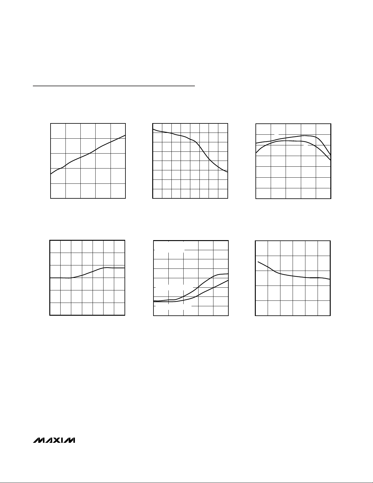
MAX9322 toc01
TEMPERATURE (°C)
SUPPLY CURRENT (mA)
603510-15
45
55
65
75
85
35
-40 85
SUPPLY CURRENT, IEE
vs. TEMPERATURE
MAX9322 toc02
FREQUENCY (MHz)
OUTPUT AMPLITUDE (mV)
800600400 140012001000200
100
200
300
400
500
600
700
800
0
0 1600
OUTPUT AMPLITUDE, V
OH - VOL
vs. FREQUENCY
TRANSITION TIME vs. TEMPERATURE
MAX9322 toc03
TEMPERATURE (°C)
TRANSITION TIME (ps)
603510-15
210
220
230
240
250
260
270
200
-40 85
t
F
t
R
MAX9322 toc04
V
IHD
- VEE (V)
PROPAGATION DELAY (ps)
3.02.72.42.11.81.5
885
890
895
900
905
910
880
1.2 3.3
PROPAGATION DELAY vs. HIGH VOLTAGE
OF DIFFERENTIAL INPUT, V
IHD
MAX9322 toc05
TEMPERATURE (°C)
PROPAGATION DELAY (ps)
603510-15
940
960
980
880
900
920
1000
1020
860
-40 85
PROPAGATION DELAY vs. TEMPERATURE
SINGLE-ENDED CLOCK
DIFFERENTIAL CLOCK
V
IH2
= VCC = 1.15V
V
IL2
= VCC = 1.48V
750
790
830
870
910
950
01.00.5 1.5 2.0 2.5 3.0
PROPAGATION DELAY
vs. DIFFERENTIAL INPUT VOLTAGE
MAX9322 toc06
DIFFERENTIAL INPUT VOLTAGE (VIHD - VILD) (V)
PROPAGATION DELAY (ps)
Typical Operating Characteristics
(VCC- VEE= 3.3V, V
IHD
= VCC- 1V, V
ILD
= VCC- 1.5V, VID= 500mV, CLK_SEL = 0, FSEL_ = 0, fIN= 600MHz, TA= +25°C, unless
otherwise noted.)
Page 6
MAX9322
LVECL/LVPECL 1:15 Differential
Divide-by-1/Divide-by-2 Clock Driver
6 _______________________________________________________________________________________
Pin Description
PIN
TQFP QFN
FUNCTION
1 2, 3 V
CC
Positive Power Supply. Powers input circuitry. Bypass each VCC to VEE with a 0.01µF
and 0.1µF capacitor. Place the capacitors as close to the device as possible with the
smaller value capacitor closest to the device.
24MR
Single-Ended Master Reset. A high on MR sets all outputs to differential zero. A low on
MR enables all outputs. MR is pulled to V
EE
through a 75kΩ resistor.
35
Single-Ended Frequency Select A. Selects the output frequency for bank A. Bank A
consists of two differential outputs. A low on FSELA selects divide-by-1. A high on
FSELA selects divide-by-2. FSELA is pulled to V
EE
through a 75kΩ resistor.
46
Single-Ended Frequency Select B. Selects the output frequency for bank B. Bank B
consists of three differential outputs. A low on FSELB selects divide-by-1. A high on
FSELB selects divide-by-2. FSELB is pulled to VEE through a 75kΩ resistor.
5 7 CLK0 Noninverting Clock 0 Input. CLK0 is pulled to VEE through 75kΩ resistors.
68CLK0 Inverting Clock 0 Input. CLK0 is pulled to VCC and to VEE through a 75kΩ resistor.
79
Single-Ended Clock Selector Input. A low on CLK_SEL selects CLK0. A high on
CLK_SEL selects CLK1. CLK_SEL is pulled to V
EE
through a 75kΩ resistor.
8 10 CLK1 Noninverting Clock 1 Input. CLK1 is pulled to VEE through a 75kΩ resistor.
911CLK1 Inverting Clock 1 Input. CLK1 is pulled to VCC and to VEE through 75kΩ resistors.
10 12 V
BB
Reference Voltage Output. Connect V
BB
to CLK_ or CLK_ to provide a reference for
single-ended operation. When used, bypass with a 0.01µF ceramic capacitor to V
CC
;
otherwise leave open.
11 13
Single-Ended Frequency Select C. Selects the output frequency for bank C. Bank C
consists of four differential outputs. A low on FSELC selects divide-by-1. A high on
FSELC selects divide-by-2. FSELC is pulled to VEE through a 75kΩ resistor.
12 14
Single-Ended Frequency Select D. Selects the output frequency for bank D. Bank D
consists of six differential outputs. A low on FSELD selects divide-by-1. A high on
FSELD selects divide-by-2. FSELD is pulled to V
EE
through a 75kΩ resistor.
13 15, 16 V
EE
Negative Power-Supply Input
14, 27, 30,
39, 40, 47,
52
19, 20, 33,
36, 37, 40,
49, 50, 53,
V
CCO
Output Driver Positive Power Supply. Powers device output drivers. Bypass each V
CCO
to VEE with a 0.01µF and 0.1µF capacitor. Place the capacitors as close to the device
as possible with the smaller value capacitor closest to the device.
15 21 QD5 Inverting QD5 Output. Typically terminate with 50Ω resistor to VCC - 2V.
16 22 QD5 Noninverting QD5 Output. Typically terminate with 50Ω resistor to VCC - 2V.
17 23 QD4 Inverting QD4 Output. Typically terminate with 50Ω resistor to VCC - 2V.
18 24 QD4 Noninverting QD4 Output. Typically terminate with 50Ω resistor to VCC - 2V.
NAME
FSELA
54, 61, 66, 67
FSELB
CLK_SEL
FSELC
FSELD
Page 7
MAX9322
LVECL/LVPECL 1:15 Differential
Divide-by-1/Divide-by-2 Clock Driver
_______________________________________________________________________________________ 7
Pin Description (continued)
PIN
TQFP QFN
FUNCTION
19 25 QD3 Inverting QD3 Output. Typically terminate with 50Ω resistor to VCC - 2V.
20 26 QD3 Noninverting QD3 Output. Typically terminate with 50Ω resistor to VCC - 2V.
21 27 QD2 Inverting QD2 Output. Typically terminate with 50Ω resistor to VCC - 2V.
22 28 QD2 Noninverting QD2 Output. Typically terminate with 50Ω resistor to VCC - 2V.
23 29 QD1 Inverting QD1 Output. Typically terminate with 50Ω resistor to VCC - 2V.
24 30 QD1 Noninverting QD1 Output. Typically terminate with 50Ω resistor to VCC - 2V.
25 31 QD0 Inverting QD0 Output. Typically terminate with 50Ω resistor to VCC - 2V.
26 32 QD0 Noninverting QD0 Output. Typically terminate with 50Ω resistor to VCC - 2V.
28, 29
1, 17, 18, 34,
35, 38, 39,
51, 52, 68
N.C. No Connection. Not internally connected.
31 41 QC3 Inverting QC3 Output. Typically terminate with 50Ω resistor to VCC - 2V.
32 42 QC3 Noninverting QC3 Output. Typically terminate with 50Ω resistor to VCC - 2V.
33 43 QC2 Inverting QC2 Output. Typically terminate with 50Ω resistor to VCC - 2V.
34 44 QC2 Noninverting QC2 Output. Typically terminate with 50Ω resistor to VCC - 2V.
35 45 QC1 Inverting QC1 Output. Typically terminate with 50Ω resistor to VCC - 2V.
36 46 QC1 Noninverting QC1 Output. Typically terminate with 50Ω resistor to VCC - 2V.
37 47 QC0 Inverting QC0 Output. Typically terminate with 50Ω resistor to VCC - 2V.
38 48 QC0 Noninverting QC0 Output. Typically terminate with 50Ω resistor to VCC - 2V.
41 55 QB2 Inverting QB2 Output. Typically terminate with 50Ω resistor to VCC - 2V.
42 56 QB2 Noninverting QB2 Output. Typically terminate with 50Ω resistor to VCC - 2V.
43 57 QB1 Inverting QB1 Output. Typically terminate with 50Ω resistor to VCC - 2V.
44 58 QB1 Noninverting QB1 Output. Typically terminate with 50Ω resistor to VCC - 2V.
45 59 QB0 Inverting QB0 Output. Typically terminate with 50Ω resistor to V
C
C
- 2V.
46 60 QB0 Noninverting QB0 Output. Typically terminate with 50Ω resistor to VCC - 2V.
48 62 QA1 Inverting QA1 Output. Typically terminate with 50Ω resistor to VCC - 2V.
49 63 QA1 Noninverting QA1 Output. Typically terminate with 50Ω resistor to VCC - 2V.
50 64 QA0 Inverting QA0 Output. Typically terminate with 50Ω resistor to VCC - 2V.
51 65 QA0 Noninverting QA0 Output. Typically terminate with 50Ω resistor to VCC - 2V.
—EPV
EE
The exposed pad of the QFN package is internally connected to VEE. Refer to
Application Note HFAN-08.1.
NAME
Page 8
MAX9322
LVECL/LVPECL 1:15 Differential
Divide-by-1/Divide-by-2 Clock Driver
8 _______________________________________________________________________________________
CLK_
CLK_
Q_
V
OH
V
OL
V
IH2
V
IL2
V
BB
VOH - V
OL
t
PHLS
t
PLHS
MR, FSEL_, CLK_SEL
V
IH1
V
IL1
V
BB
(CLK_ IS CONNECTED TO VBB)
Q_
Figure 1. Timing Diagram for Single-Ended Inputs
CLK_
CLK_
Q_
t
PLHD
t
PHLD
V
IHD
- V
ILD
V
IHD
V
ILD
0V (DIFFERENTIAL) 0V (DIFFERENTIAL)
20%
80%
20%
80%
t
R
t
F
V
OL
V
OH
VOH - V
OL
Q_
Q_ - Q_
V
OH
- V
OL
Figure 2. Timing Diagram for Differential Inputs
Page 9

Detailed Description
The MAX9322 low-skew 1:15 differential clock driver
reproduces or divides one of two differential input
clocks at 15 differential outputs. An input multiplexer
selects from one of two input clocks with input frequency operation in excess of 1.0GHz. The 15 outputs are
arranged into four banks with 2, 3, 4, and 6 outputs,
respectively. Each output bank is individually programmable to provide a divide-by-1 or divide-by-2 frequency function.
LVECL/LVPECL Operation
Output levels are referenced to VCCand are LVPECL or
LVECL, depending on the level of the V
CC
supply. With
VCCconnected to a positive supply and VEEconnected
to ground, the outputs are LVPECL. The outputs are
LVECL when VCCis connected to ground and VEEis
connected to a negative supply. When interfacing to
differential LVPECL signals, the VCCrange is 2.375V to
3.8V (VEE= 0), allowing high-performance clock distribution in systems with nominal 2.5V and 3.3V supplies.
When interfacing to differential LVECL, the VEErange is
-2.375V to -3.8V (V
CC
= 0).
Control Inputs (FSEL_, CLK_SEL, MR)
The MAX9322 provides four output banks: A, B, C, and
D. Bank A consists of two differential output pairs. Bank
B consists of three differential output pairs. Bank C
consists of four differential output pairs. Bank D consists of six differential output pairs. FSEL_ selects the
output clock frequency for a bank. A low on FSEL_
selects divide-by-1 frequency operation while a high on
FSEL_ selects divide-by-2 operation. CLK_SEL selects
CLK0 or CLK1 as the input signal. A low on CLK_SEL
selects CLK0 while a high selects CLK1.
Master reset (MR) enables all outputs. CLK_SEL and
FSEL_ are asynchronous. Changes to the control inputs
(CLK_SEL, FSEL_) or on power-up cause indeterminate
output states requiring a MR assertion to resynchronize
any divide-by-2 outputs (Figure 4). A low on MR activates
all outputs for normal operation. A high on MR resets all
outputs to differential low condition. See Table 1.
Input Termination Resistors
Differential inputs CLK_ and CLK_ are biased to guar-
antee a known state (differential low) if the inputs are
left open. CLK_ is internally pulled to VEEthrough a
75kΩ resistor. CLK_ is internally pulled to VCCand to
VEEthrough 75kΩ resistors.
Single-ended inputs FSEL_, MR, and CLK_SEL are
internally pulled to VEEthrough a 75kΩ resistor.
Differential Clock Input
The MAX9322 accepts two differential or single-ended
clock inputs, CLK0/CLK0 and CLK1/CLK1. CLK_SEL
selects between CLK0/CLK0 and CLK1/CLK1. A low on
CLK_SEL selects CLK0/CLK0. A high on CLK_SEL
selects CLK1/CLK1. See Table 1.
Differential CLK_ inputs must be at least VBB±95mV to
switch the outputs to the VOHand VOLlevels specified
in the DC Electrical Characteristics table. The maximum
magnitude of the differential signal applied to the differential clock input is the lower of (VCC- VEE) and 3.0V.
This limit also applies to the difference between any reference voltage input and a single-ended input.
Specifications for the high and low voltages of a differential input (V
IHD
and V
ILD
) and the differential input
voltage (V
IHD
- V
ILD
) apply simultaneously.
MAX9322
LVECL/LVPECL 1:15 Differential
Divide-by-1/Divide-by-2 Clock Driver
MR
Q_
Q_
t
PD
V
IH
V
IL
V
OL
V
OH
V
BB
Table 1. Function Table
*A master reset is required following power-up or changes to
input functions to prevent indeterminant output states.
Figure 3. Timing Diagram for MR
_______________________________________________________________________________________ 9
PIN
FSEL_ Divide-by-1 Divide-by-2
CLK_SEL CLK0 CLK1
MR* Active Reset
FUNCTION
LOW OR OPEN HIGH
Page 10
MAX9322
LVECL/LVPECL 1:15 Differential
Divide-by-1/Divide-by-2 Clock Driver
10 ______________________________________________________________________________________
CLK_
MR
Q_(÷1)
Q_(÷2)
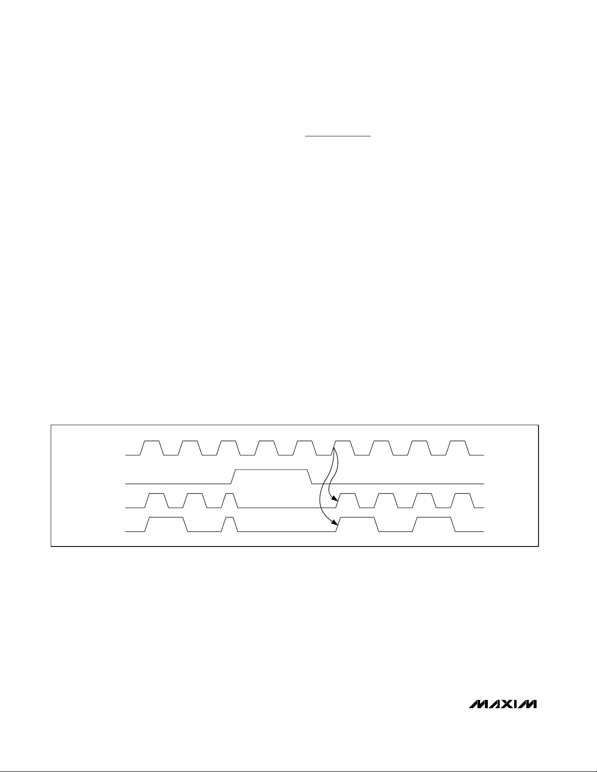
Figure 4. Timing Diagram for MR Resynchronization
Single-Ended Inputs and V
BB
The differential clock input can be configured to accept
a single-ended input when operating at VCC- VEE=
3.0V to 3.8V. Connect VBBto the inverting or noninverting input of the differential input as a reference for single-ended operation. The differential CLK_ input is
converted to a noninverting, single-ended input by connecting VBBto CLK_ and connecting the single-ended
input signal to CLK. Similarly, an inverting configuration
is obtained by connecting VBBto CLK_ and connecting
the single-ended input to CLK_.
The single-ended inputs FSEL_, CLK_SEL, and MR are
internally referenced to VBB. All single-ended inputs
(FSEL_, CLK_SEL, MR, and any CLK_ in single-ended
mode) can be driven to VCCand VEEor with a singleended LVPECL/LVECL signal. The single-ended input
must be at least VBB±95mV to switch the outputs to the
VOHand VOLlevels specified in the DC Electrical
Characteristics table. When using the VBBreference
output, bypass VBBwith a 0.01µF ceramic capacitor to
VCC. Leave VBBopen when not used. The VBBreference can source or sink 0.5mA. Use VBBas a reference for the same device only.
Applications Information
Supply Bypassing
Bypass each V
CC
and V
CCO
to VEEwith high-frequency
surface-mount ceramic 0.01µF and 0.1µF capacitors in
parallel as close to the device as possible, with the
0.01µF capacitor closest to the device. Use multiple
parallel vias to minimize parasitic inductance. When
using the VBBreference output, bypass VBBto V
CC
with a 0.01µF ceramic capacitor.
Controlled-Impedance Traces
Input and output trace characteristics affect the performance of the MAX9322. Connect input and output signals with 50Ω characteristic impedance traces.
Minimize the number of vias to prevent impedance discontinuities. Reduce reflections by maintaining the 50Ω
characteristic impedance through cables and connectors. Reduce skew within a differential pair by matching
the electrical length of the traces.
Output Termination
Terminate outputs with 50Ω to VCC- 2V or use an
equivalent Thevenin termination. When a single-ended
signal is taken from a differential output, terminate both
outputs. For example, if QA0 is used as a single-ended
output, terminate both QA0 and QA0.
Page 11
MAX9322
LVECL/LVPECL 1:15 Differential
Divide-by-1/Divide-by-2 Clock Driver
______________________________________________________________________________________ 11
0
1
0
1
0
1
0
1
÷1
÷2
75kΩ
75kΩ
75kΩ
V
EE
V
CC
V
EE
75kΩ
75kΩ
75kΩ
V
EE
V
CC
V
EE
75kΩ
V
EE
75kΩ
V
EE
75kΩ
V
EE
75kΩ
V
EE
75kΩ
V
EE
75kΩ
V
EE
FSELA
CLK0
CLK0
CLK1
CLK1
CLK_SEL
MR
FSELB
FSELC
FSELD
V
BB
BANK A
BANK B
BANK C
BANK D
QA0
QA0
QA1
QA1
QB0
QB0
QB1
QB1
QB2
QB2
QC0
QC0
QC1
QC1
QC2
QC2
QC3
QC3
QD0
QD0
QD1
QD1
QD2
QD2
QD3
QD3
QD4
QD4
QD5
QD5
MAX9322
Functional Diagram
Page 12

MAX9322
LVECL/LVPECL 1:15 Differential
Divide-by-1/Divide-by-2 Clock Driver
12 ______________________________________________________________________________________
5859606162 5455565763
38
39
40
41
42
43
44
45
46
47
CLK1
VCCO
QA1
QFN*
TOP VIEW
QA1
VCCO
QB0
QB0
QB1
QB1
QB2
QB2
VCCO
5253
VCCO
N.C.
N.C.
QD5
VCCO
QD4
QD5
QD3
QD4
QD2
QD3
QD1
QD2
QD0
QD1
QD0
QC0
QC1
QC1
QC2
QC2
QC3
QC3
VCCO
N.C.
N.C.
35
36
37
VCCO
VCCO
N.C.
CLK1
CLK_SEL
CLK0
CLK0
FSELB
V
EE
V
EE
FSELD
FSELC
V
BB
FSELA
MR
V
CC
V
CC
48 QC0
N.C.
64
QA0
656667
VCCO
VCCO
QA0
68
N.C.
2322212019 2726252418 2928 323130
VCCO
N.C.
3433
49
50
VCCO
VCCO
51 N.C.
11
10
9
8
7
6
5
4
3
2
16
15
14
13
12
1
N.C. 17
MAX9322
THE EXPOSED PAD OF THE QFN PACKAGE MUST BE SOLDERED TO V
EE
FOR PROPER THERMAL AND ELECTRICAL OPERATION OF THE MAX9322.
Pin Configurations (continued)
Chip Information
TRANSISTOR COUNT: 2063
PROCESS: Bipolar
Page 13

MAX9322
LVECL/LVPECL 1:15 Differential
Divide-by-1/Divide-by-2 Clock Driver
Maxim cannot assume responsibility for use of any circuitry other than circuitry entirely embodied in a Maxim product. No circuit patent licenses are
implied. Maxim reserves the right to change the circuitry and specifications without notice at any time.
Maxim Integrated Products, 120 San Gabriel Drive, Sunnyvale, CA 94086 408-737-7600 ____________________ 13
© 2007 Maxim Integrated Products is a registered trademark of Maxim Integrated Products, Inc.
PACKAGE OUTLINE
52L TQFP, 10x10x1.0 MM
1
1
21-0146
A
REV.DOCUMENT CONTROL NO.APPROVAL
PROPRIETARY INFORMATION
TITLE:
TOP VIEW
0.65 BSC
NOM
0.10
-
-
0.32
12.00
10.00 BSC
10.00 BSC
0.60
12.00
e
0.45L
11.80E
E1
D1
DIM
11.80
0.09
0.05
c
D
A1
b
MIN
-A
0.75
12.20
0.15
0.20
12.20
1.20
MAX
A2
0.95 1.00 1.05
SEATING PLANE
E1
A1
A2
SEE DETAIL "A"
52
c
A
1
SEE
4
E1
b
e
4
D1
D1
D
GAGE PLANE
1.00 REF
DETAIL A
L
0-7∞
0.25
0∞ MIN.
E
0.22 0.38
NOTE 2
52L TQFP.EPS
Revision History
Pages changed at Rev 2: 1, 5, 13
Package Information
(The package drawing(s) in this data sheet may not reflect the most current specifications. For the latest package outline information,
go to www.maxim-ic.com/packages
.)
 Loading...