

Page 1
For pricing delivery, and ordering information please contact Maxim/Dallas Direct! at
1-888-629-4642, or visit Maxim’s website at www.maxim-ic.com.
General Description
The MAX9320B low-skew, 1-to-2 differential driver is
designed for clock and data distribution. The input is
reproduced at two differential outputs. The differential
input can be adapted to accept single-ended inputs by
applying an external reference voltage.
The MAX9320B features ultra-low propagation delay
(208ps), part-to-part skew (20ps), and output-to-output
skew (6ps) with 30mA maximum supply current, making this device ideal for clock distribution. For interfacing to differential PECL and LVPECL signals, this
device operates over a +3.0V to +5.5V supply range,
allowing high-performance clock or data distribution in
systems with a nominal 3.3V or 5V supply. For differential ECL and LVECL operation, this device operates
from a -3.0V to -5.5V supply.
The MAX9320B is offered in industry-standard 8-pin
TSSOP and SO packages.
Applications
Precision Clock Distribution
Low-Jitter Data Repeater
Protection Switching
Features
♦ Improved Second Source of the MC10EP11D
♦ +3.0V to +5.5V Differential PECL/LVPECL
Operation
♦ -3.0V to -5.5V ECL/LVECL Operation
♦ Low 22mA Supply Current
♦ 20ps Part-to-Part Skew
♦ 6ps Output-to-Output Skew
♦ 208ps Propagation Delay
♦ Minimum 300mV Output at 3GHz
♦ Outputs Low for Open Input
♦ ESD Protection >2kV (Human Body Model)
MAX9320B
1:2 Differential PECL/ECL/LVPECL/LVECL
Clock and Data Driver
________________________________________________________________ Maxim Integrated Products 1
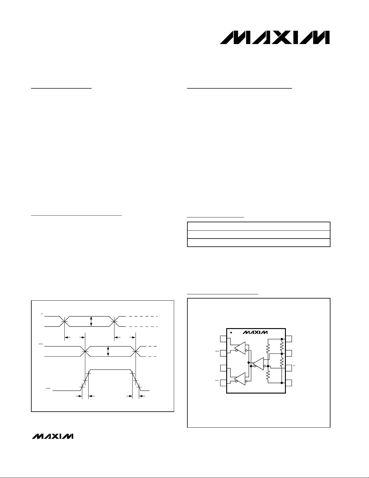
Pin Configuration
19-2383; Rev 1; 11/03
Ordering Information
Figure 1. Differential Transition Time and Propagation Delay
Timing Diagram
PART TEMP RANGE PIN-PACKAGE
MAX9320BESA -40°C to +85°C 8 SO
MAX9320BEUA -40°C to +85°C 8 TSSOP
D
D
Q_
Q
(Q_) - (Q_)
t
PLHD
20%
V
- V
IHD
80%
0V (DIFFERENTIAL)
t
R
ILD
t
PHLD
V
- V
OH
OL
80%
0V (DIFFERENTIAL)
t
F
20%
V
IHD
V
ILD
Q0
1
V
OH
Q0
V
OL
2
Q1
3
Q1
4
MAX9320B
50kΩ
100kΩ
80kΩ
60kΩ
V
8
CC
D
7
D
6
V
5
EE
TSSOP/SO
Page 2
MAX9320B
1:2 Differential PECL/ECL/LVPECL/LVECL
Clock and Data Driver
2 _______________________________________________________________________________________
ABSOLUTE MAXIMUM RATINGS
DC ELECTRICAL CHARACTERISTICS
(VCC- VEE= 3.0V to 5.5V, outputs loaded with 50Ω ±1% to VCC- 2V. Typical values are at VCC- VEE= 5.0V, V
IHD
= VCC- 1.0V, V
ILD
= VCC- 1.5V, unless otherwise noted.) (Notes 1, 2, 3)
Stresses beyond those listed under “Absolute Maximum Ratings” may cause permanent damage to the device. These are stress ratings only, and functional
operation of the device at these or any other conditions beyond those indicated in the operational sections of the specifications is not implied. Exposure to
absolute maximum rating conditions for extended periods may affect device reliability.
VCCto VEE.............................................................................+6V
D or D....................................................V
EE
- 0.3V to VCC+ 0.3V
D or D with the Other Floating............. V
CC
- 5.0V to VCC+ 0.3V
D to D .................................................................................±3.0V
Continuous Output Current .................................................50mA
Surge Output Current........................................................100mA
Continuous Output Power Dissipation (TA= +70°C)
8-Pin TSSOP
(derate 4.5mW/°C above +70°C).................................362mW
8-Pin SO
(derate 5.9mW/°C above +70°C).................................471mW
Junction-to-Ambient Thermal Resistance in Still Air
8-Pin TSSOP ............................................................+221°C/W
8-Pin SO...................................................................+170°C/W
Junction-to-Ambient Thermal Resistance with 500
LFPM Airflow
8-Pin TSSOP ............................................................+155°C/W
8-Pin SO.....................................................................+99°C/W
Junction-to-Case Thermal Resistance
8-Pin TSSOP ..............................................................+39°C/W
8-Pin SO.....................................................................+40°C/W
Operating Temperature Range ...........................-40°C to +85°C
Junction Temperature......................................................+150°C
Storage Temperature Range .............................-65°C to +150°C
ESD Protection
Human Body Model (D, D, Q_, Q_) .................................>2kV
Soldering Temperature (10s) ...........................................+300°C
PARAMETER SYM BOL CONDITIONS
DIFFERENTIAL INPUT (D, D)
High Voltage of
Differential
Input
Low Voltage of
Differential
Input
Differential
Input Voltage
Input High
Current
D Input Low
Current
D Input Low
Current
DIFFERENTIAL OUTPUTS (Q_, Q__)
Single-Ended
Output High
Voltage
V
IHD
V
ILD
V
-
IHD
V
ILD
I
IH
I
ILD
I
ILD
V
OH
VCC - VEE ≤ 3.8V -100 +100 -100 +100 -100 +100
VCC - VEE ≥ 3.8V -140 +140 -140 +140 -140 +140
VCC - VEE ≤ 3.8V -150 +150 -150 +150 -150 +150
VCC - VEE ≥ 3.8V -175 +175 -175 +175 -175 +175
Figure 1
- 1.135
-40°C +25°C +85°C
MIN TYP MAX MIN TYP MAX MIN TYP MAX
V
EE
+ 1.2
V
EE
0.1 3.0 0.1 3.0 0.1 3.0 V
V
CC
V
V
CC
V
CC
- 0.1
150 150 150 µA
V
CC
- 0.885
EE
+ 1.2
V
EE
V
CC
- 1.07
V
V
- 0.1
V
- 0.82
CC
CC
CC
V
EE
+ 1.2
V
EE
V
CC
- 1.01
V
CC
V
CC
- 0.1
V
CC
- 0.76
UNITS
V
V
µA
µA
V
Page 3
MAX9320B
1:2 Differential PECL/ECL/LVPECL/LVECL
Clock and Data Driver
_______________________________________________________________________________________ 3
DC ELECTRICAL CHARACTERISTICS (continued)
(VCC- VEE= 3.0V to 5.5V, outputs loaded with 50Ω ±1% to VCC- 2V. Typical values are at VCC- VEE= 5.0V, V
IHD
= VCC- 1.0V, V
ILD
= VCC- 1.5V, unless otherwise noted.) (Notes 1, 2, 3)
AC ELECTRICAL CHARACTERISTICS
(VCC- VEE= 3.0V to 5.5V, outputs loaded with 50Ω ±1% to VCC- 2V, input frequency ≤ 1.5GHz, input transition time = 125ps (20% to
80%), V
IHD
= VEE+ 1.2V to VCC, V
ILD
= VEEto VCC- 0.15V, V
IHD
- V
ILD
= 0.15V to 3.0V. Typical values are at VCC- VEE= 5.0V, V
IHD
= VCC- 1V, V
ILD
= VCC- 1.5V, unless otherwise noted.) (Note 5)
PARAMETER SYMBOL CONDITIONS
Single-Ended
Output Low
Voltage
Differential
Output Voltage
POWER SUPPLY
Supply Current I
V
- V
V
OL
OH
EE
Figure 1
Figure 1 550 550 550 mV
OL
(Note 4) 20 28 22 28 23 30 mA
- 1.935
-40°C +25°C +85°C
MIN TYP MAX MIN TYP MAX MIN TYP MAX
V
CC
V
- 1.685
CC
V
CC
- 1.87
V
CC
- 1.62
V
CC
- 1.81
V
CC
- 1.56
UNITS
V
PARAMETER SYMBOL CONDITIONS
Differential
Input-toOutput Delay
t
PLHD
t
PHLD
MIN TYP MAX MIN TYP MAX MIN TYP MAX
,
Figure 1 145 220 265 155 208 265 160 203 270 ps
-40°C +25°C +85°C
UNITS
Output-toOutput Skew
Part-to-Part
Skew
Added
Random Jitter
Added
Deterministic
Jitter
t
SKOO
t
SKPP
t
t
(Note 6) 6 30 6 30 6 30 ps
(Note 7) 20 120 20 110 20 110 ps
fIN = 1.5GHz, clock
pattern (Note 8)
RJ
fIN = 3.0GHz, clock
pattern (Note 8)
3.0Gbps
23
2
DJ
(Note 8)
- 1 PRBS pattern
1.7 2.8 1.7 2.8 1.7 2.8
0.6 1.5 0.6 1.5 0.6 1.5
57 80 57 80 57 80
ps
(RMS)
ps
(
P-P
)
Page 4

Typical Operating Characteristics
(VCC= 5V, VEE= 0, input transition time = 125ps (20% to 80%), V
IHD
= VCC- 1V, V
ILD
= VCC- 1.5V, fIN= 1.5GHz, outputs loaded with
50Ω to V
CC
- 2V, TA= +25°C, unless otherwise noted.)
Note 1: Measurements are made with the device in thermal equilibrium.
Note 2: Current into a pin is defined as positive. Current out of a pin is defined as negative.
Note 3: DC parameters production tested at T
A
= +25°C. Guaranteed by design and characterization over the full operating temper-
ature range.
Note 4: All pins open except V
CC
and VEE.
Note 5: Guaranteed by design and characterization. Limits are set at ±6 sigma.
Note 6: Measured between outputs of the same part at the signal crossing points for a same-edge transition.
Note 7: Measured between outputs of different parts at the signal crossing points under identical conditions for a same-edge transition.
Note 8: Device jitter added to the input signal.
MAX9320B
1:2 Differential PECL/ECL/LVPECL/LVECL
Clock and Data Driver
4 _______________________________________________________________________________________
AC ELECTRICAL CHARACTERISTICS (continued)
(VCC- VEE= 3.0V to 5.5V, outputs loaded with 50Ω ±1% to VCC- 2V, input frequency ≤ 1.5GHz, input transition time = 125ps (20% to
80%), V
IHD
= VEE+ 1.2V to VCC, V
ILD
= VEEto VCC- 0.15V, V
IHD
- V
ILD
= 0.15V to 3.0V. Typical values are at VCC- VEE= 5.0V, V
IHD
= VCC- 1V, V
ILD
= VCC- 1.5V, unless otherwise noted.) (Note 5)
TRANSITION TIME vs. TEMPERATURE
MAX9320B toc03
TEMPERATURE (°C)
TRANSITION TIME (ps)
603510-15
85
90
95
100
105
110
80
-40 85
t
R
t
F
OUTPUT AMPLITUDE, VOH - VOL
vs. FREQUENCY
MAX9320B toc02
FREQUENCY (MHz)
OUTPUT AMPLITUDE (V)
30002500500 1000 1500 2000
0.1
0.2
0.3
0.4
0.5
0.6
0.7
0.8
0
03500
SUPPLY CURRENT, I
EE
vs. TEMPERATURE
MAX9320B toc01
TEMPERATURE (°C)
SUPPLY CURRENT (mA)
603510-15
16
17
18
19
20
21
22
23
24
25
15
-40 85
PARAMETER SYMBOL CONDITIONS
Switching
Frequency
Output
Rise/Fall Time
(20% to 80%)
f
MAX
t
, t
R
F
-40°C +25°C +85°C
MIN TYP MAX MIN TYP MAX MIN TYP MAX
VOH - VOL ≥ 300mV,
clock pattern,
3.0 3.0 3.0
Figure 1
VOH - VOL ≥ 550mV,
clock pattern,
2.0 2.0 2.0
Figure 1
Figure 1 50 95 120 50 98 120 50 105 120 ps
UNITS
GHz
Page 5

MAX9320B
1:2 Differential PECL/ECL/LVPECL/LVECL
Clock and Data Driver
_______________________________________________________________________________________ 5
Typical Operating Characteristics (continued)
(VCC= 5V, VEE= 0, input transition time = 125ps (20% to 80%), V
IHD
= VCC- 1V, V
ILD
= VCC- 1.5V, fIN= 1.5GHz, outputs loaded with
50Ω to V
CC
- 2V, TA= +25°C, unless otherwise noted.)
Pin Description
PROPAGATION DELAY vs. HIGH VOLTAGE
OF DIFFERENTIAL INPUT, V
220
215
210
205
200
PROPAGATION DELAY (ps)
195
190
1.2 5.6
t
PLHD
t
PHLD
V
V
IHD
- V
= 0.5V
IHD
ILD
5.24.84.44.03.63.22.82.42.01.6
(V)
IHD
PIN NAME FUNCTION
1 Q0 Noninverting Q0 Output. Typically terminate with 50Ω resistor to VCC - 2V.
2 Q0 Inverting Q0 Output. Typically terminate with 50Ω resistor to VCC - 2V.
3 Q1 Noninverting Q1 Output. Typically terminate with 50Ω resistor to VCC - 2V.
4 Q1 Inverting Q1 Output. Typically terminate with 50Ω resistor to VCC - 2V.
5VEENegative Supply Voltage
6 D Inverting Differential Input. 50kΩ pullup to VCC and 100kΩ pulldown to VEE.
7 D Noninverting Differential Input. 80kΩ pullup to VCC and 60kΩ pulldown to VEE.
8V
CC
Positive Supply Voltage. Bypass from VCC to VEE with 0.1µF and 0.01µF ceramic capacitors. Place the
capacitors as close to the device as possible with the smaller value capacitor closest to the device.
MAX9320B toc04
PROPAGATION DELAY vs. TEMPERATURE
240
230
220
210
200
190
PROPAGATION DELAY (ps)
180
170
160
-40 85
t
PLHD
t
PHLD
TEMPERATURE (°C)
MAX9320B toc05
6035-15 10
Page 6

MAX9320B
1:2 Differential PECL/ECL/LVPECL/LVECL
Clock and Data Driver
6 _______________________________________________________________________________________
Detailed Description
The MAX9320B low-skew, 1-to-2 differential driver is
designed for clock and data distribution. For interfacing
to differential PECL and LVPECL signals, this device
operates over a +3.0V to +5.5V supply range, allowing
high-performance clock and data distribution in systems with a nominal 3.3V or 5V supply. For differential
ECL and LVECL operation, this device operates from a
-3.0V to -5.5V supply.
Inputs
The maximum magnitude of the differential input from D
to D is 3.0V. This limit also applies to the difference
between any reference voltage input and a singleended input.
The differential inputs have bias resistors that drive the
outputs to a differential low when the inputs are open.
The inverting input, D, is biased with a 50kΩ pullup to
VCCand a 100kΩ pulldown to VEE. The noninverting
input, D, is biased with an 80kΩ pullup to V
CC
and a
60kΩ pulldown to VEE.
Specifications for the high and low voltages of the differential input (V
IHD
and V
ILD
) and the differential input
voltage (V
IHD
- V
ILD
) apply simultaneously (V
ILD
cannot
be higher than V
IHD
).
Outputs
Output levels are referenced to VCCand are considered PECL/LVPECL or ECL/LVECL, depending on the
level of the VCCsupply. With VCCconnected to a positive supply and VEEconnected to GND, the outputs are
PECL/LVPECL. The outputs are ECL/LVECL when V
CC
is connected to GND and VEEis connected to a negative supply.
A differential input of at least ±100mV switches the outputs to the V
OH
and VOLlevels specified in the DC
Electrical Characteristics table.
Applications Information
Supply Bypassing
Bypass VCCto VEEwith high-frequency surface-mount
ceramic 0.1µF and 0.01µF capacitors in parallel as
close to the device as possible, with the 0.01µF value
capacitor closest to the device. Use multiple parallel
ground vias for low inductance.
Traces
Input and output trace characteristics affect the performance of the MAX9320B. Connect each signal of a differential input or output to a 50Ω characteristic impedance
trace. Minimize the number of vias to prevent impedance
discontinuities. Reduce reflections by maintaining the
50Ω characteristic impedance through connectors and
across cables. Reduce skew within a differential pair by
matching the electrical length of the traces.
Output Termination
Terminate outputs through 50Ω to VCC- 2V or use an
equivalent Thevenin termination. Terminate both outputs and use the same termination on each for the lowest output-to-output skew. When a single-ended signal
is taken from a differential output, terminate both outputs. For example, if Q0 is used as a single-ended output, terminate both Q0 and Q0.
Chip Information
TRANSISTOR COUNT: 182
Page 7

MAX9320B
1:2 Differential PECL/ECL/LVPECL/LVECL
Clock and Data Driver
Maxim cannot assume responsibility for use of any circuitry other than circuitry entirely embodied in a Maxim product. No circuit patent licenses are
implied. Maxim reserves the right to change the circuitry and specifications without notice at any time.
Maxim Integrated Products, 120 San Gabriel Drive, Sunnyvale, CA 94086 408-737-7600 _____________________ 7
© 2002 Maxim Integrated Products Printed USA is a registered trademark of Maxim Integrated Products.
Package Information
(The package drawing(s) in this data sheet may not reflect the most current specifications. For the latest package outline information,
go to www.maxim-ic.com/packages.)
9LUCSP, 3x3.EPS
 Loading...