

Page 1
General Description
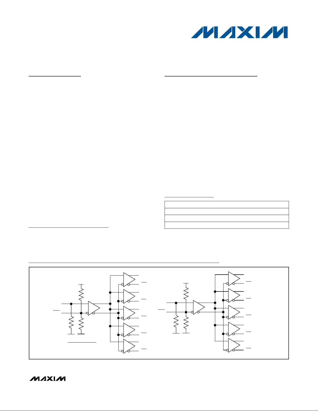
The MAX9312/MAX9314 are low skew, dual 1-to-5 differential drivers designed for clock and data distribution. These devices accept two inputs. Each input is
reproduced at five differential outputs. The differential
inputs can be adapted to accept single-ended inputs
by connecting the on-chip VBBsupply to one input as a
reference voltage.
The MAX9312/MAX9314 feature low part-to-part skew
(30ps) and output-to-output skew (12ps), making them
ideal for clock and data distribution across a backplane
or a board. For interfacing to differential HSTL and
LVPECL signals, these devices operate over a +2.25V
to +3.8V supply range, allowing high-performance clock
or data distribution in systems with a nominal +2.5V or
+3.3V supply. For differential LVECL operation, these
devices operate from a -2.25V to -3.8V supply.
The MAX9312 features an on-chip VBBreference output
of 1.425V below the positive supply voltage. The
MAX9314 offers an on-chip VBBreference output of
1.32V below the positive supply voltage.
Both devices are offered in an industry-standard 32-pin
7mm x 7mm LQFP package. In addition, the MAX9312
is offered in a space-saving 32-pin 5mm x 5mm TQFN
package.
Applications
Precision Clock Distribution
Low-Jitter Data Repeater
Features
o +2.25V to +3.8V Differential HSTL/LVPECL
Operation
o -2.25V to -3.8V Differential LVECL Operation
o 30ps (typ) Part-to-Part Skew
o 12ps (typ) Output-to-Output Skew
o 312ps (typ) Propagation Delay
o ≥ 300mV Differential Output at 3GHz
o On-Chip Reference for Single-Ended Inputs
o Output Low with Open Input
o Pin Compatible with MC100LVEP210 (MAX9312)
and MC100EP210 (MAX9314)
o Offered in Tiny QFN* Package (70% Smaller
Footprint than LQFP)
MAX9312/MAX9314
Dual 1:5 Differential LVPECL/LVECL/HSTL
Clock and Data Drivers
________________________________________________________________
Maxim Integrated Products
1
Ordering Information
19-2079; Rev 2; 4/09
For pricing, delivery, and ordering information, please contact Maxim Direct at 1-888-629-4642,
or visit Maxim’s website at www.maxim-ic.com.
Pin Configuration appears at end of data sheet.
Functional Diagram
*
Exposed pad.
+
Denotes a lead(Pb)-free/RoHS-compliant package.
PART TEMP RANGE PIN-PACKAGE
MAX9312ECJ+ -40°C to +85°C 32 LQFP
MAX9312ETJ+ -40°C to +85°C 32 TQFN-EP*
MAX9314ECJ -40°C to +85°C 32 LQFP
QB0
QB0
QB1
QB1
QB2
QB2
QB3
QB3
QB4
QB4
V
CC
75kΩ
CLKA
CLKA
75kΩ 75kΩ
V
V
EE
V
BB
EE
QA0
QA0
QA1
QA1
QA2
QA2
QA3
QA3
QA4
QA4
CLKB
CLKB
75kΩ 75kΩ
75kΩ
V
EE
V
CC
V
EE
Page 2
MAX9312/MAX9314
Dual 1:5 Differential LVPECL/LVECL/HSTL
Clock and Data Drivers
2 _______________________________________________________________________________________
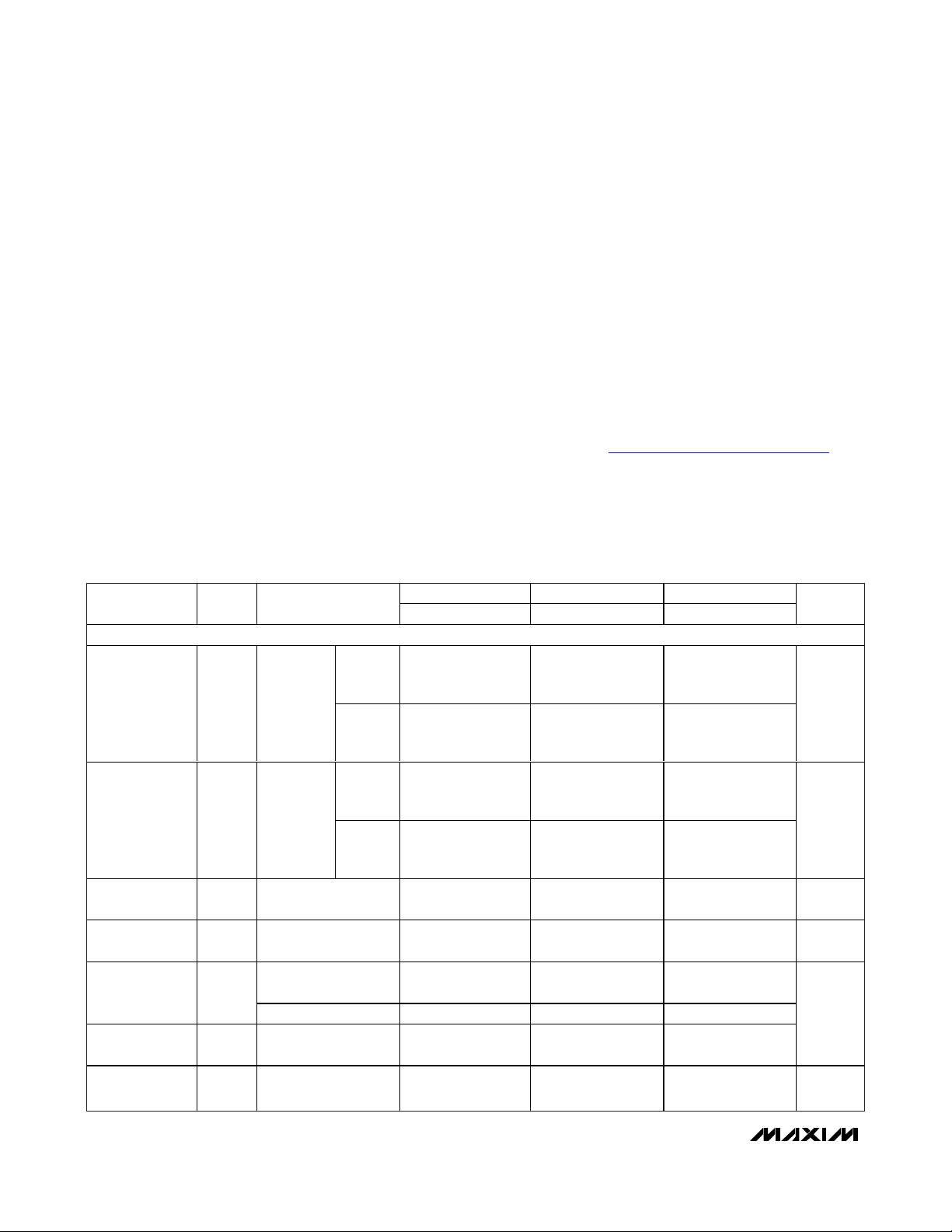
ABSOLUTE MAXIMUM RATINGS
DC ELECTRICAL CHARACTERISTICS
(VCC- VEE= +2.25V to +3.8V, outputs loaded with 50Ω ±1% to VCC- 2V.) (Notes 2–5)
Stresses beyond those listed under “Absolute Maximum Ratings” may cause permanent damage to the device. These are stress ratings only, and functional
operation of the device at these or any other conditions beyond those indicated in the operational sections of the specifications is not implied. Exposure to
absolute maximum rating conditions for extended periods may affect device reliability.
VCC- VEE...............................................................................4.1V
Inputs (CLK_, CLK_) .............................V
EE
- 0.3V to VCC+ 0.3V
CLK_ to CLK_ ....................................................................±3.0V
Continuous Output Current .................................................50mA
Surge Output Current........................................................100mA
V
BB
Sink/Source Current ...............................................±0.65mA
Continuous Power Dissipation (T
A
= +70°C)
32-Pin LQFP (derate 20.7mW/°C above +70°C) ....1652.9mW
32-Pin TQFN (derate 34.5mW/°C above +70°C)....2758.6mW
Junction-to-Case Thermal Resistance (T
JC
) (Note A)
32-Pin LQFP ................................................................12°C/W
32-Pin TQFN ..................................................................2°C/W
Junction-to-Ambient Thermal Resistance (T
JA
) (Note 1)
32-Pin LQFP .............................................................48.4°C/W
32-Pin TQFN ................................................................29°C/W
Operating Temperature Range ...........................-40°C to +85°C
Junction Temperature......................................................+150°C
Storage Temperature Range .............................-65°C to +150°C
ESD Protection
Human Body Model (CLK_, CLK_, Q_, Q_) ........................2kV
Soldering Temperature (10s) ...........................................+300°C
Note 1: Package thermal resistances were obtained using the method described in JEDEC specification JESD51-7, using a four-
layer board. For detailed information on package thermal considerations, refer to www.maxim-ic.com/thermal-tutorial
.
PARAMETER SYMBOL CONDITIONS
INPUTS (CLK_, CLK_)
-40°C +25°C +85°C
MIN MAX MIN MAX MIN MAX
UNITS
Single-Ended
Input High
Voltage
Single-Ended
Input Low
Voltage
High Voltage of
Differential Input
Low Voltage of
Differential Input
Differential Input
Voltage
Input High
Current
CLK_ Input Low
Current
V
V
V
IHD
V
ILD
V
IHD
V
ILD
I
IH
I
ILCLK
V
IH
B B
connected
to CLK_
(V
for V
IL
connected
MAX9312
B B
MAX9314
to C LK_)
V
IL
B B
connected
to CLK_
(V
for V
IL
connected
MAX9312 V
B B
MAX9314 V
to C LK_)
For VCC - VEE < 3.0V 0.095
-
V
CC
1.23
V
CC
1.165
EE
EE
VEE +
1.2
V
EE
V
CC
V
CC
VCC -
1.62
VCC -
1.475
V
CC
VCC -
0.095
V
CC
V
EE
VCC -
1.23
VCC -
1.165
V
EE
V
EE
VEE +
1.2
V
EE
-
0.095
V
CC
V
CC
VCC -
1.62
VCC -
1.475
V
CC
VCC -
0.095
V
CC
V
EE
-
For VCC - VEE ≥ 3.0V 0.095 3.0 0.095 3.0 0.095 3.0
150 150 150 µA
-10 +10 -10 +10 -10 +10 µA
VCC -
1.23
VCC -
1.165
V
EE
V
EE
VEE +
1.2
V
EE
0.095
V
CC
V
CC
VCC -
1.62
VCC -
1.475
V
CC
VCC -
0.095
V
CC
V
EE
V
V
V
V
V
Page 3
MAX9312/MAX9314
Dual 1:5 Differential LVPECL/LVECL/HSTL
Clock and Data Drivers
_______________________________________________________________________________________ 3
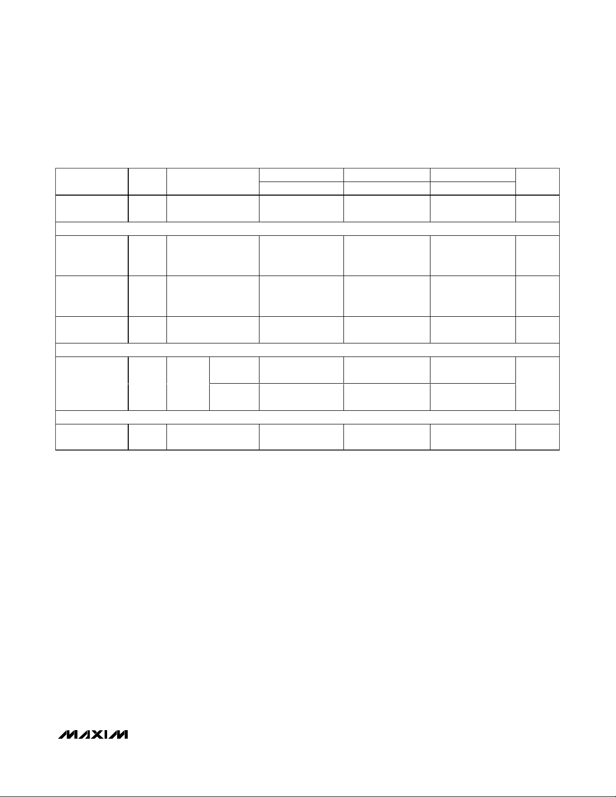
DC ELECTRICAL CHARACTERISTICS (continued)
(VCC- VEE= +2.25V to +3.8V, outputs loaded with 50Ω ±1% to VCC- 2V.) (Notes 2–5)
PARAMETER SYMBOL CONDITIONS
CLK_ Input Low
Current
OUTPUTS (Q__, Q__)
Single-Ended
Output High
Voltage
Single-Ended
Output Low
Voltage
Differential
Output Voltage
REFERENCE (VBB)
Reference
Voltage Output
(Note 6)
POWER SUPPLY
Supply Current
(Note 7)
I
ILCLK
V
OH
V
OL
VOH -
V
OL
V
BB
I
EE
Figure 1
Figure 1
Figure 1 670 950 670 950 670 950 mV
MAX9312
IBB =
±0.5mA
MAX9314
-40°C +25°C +85°C
MIN MAX MIN MAX MIN MAX
-150 -150 -150 µA
V
-
CC
1.025
V
CC
-1.930
V
CC
1.525
V
CC
1.38
VCC -
0.900
-
VCC -
1.695
-
VCC -
1.325
-
VCC -
1.26
75 82 95 mA
VCC -
1.025
VCC -
-1.930
VCC -
1.525
VCC -
1.38
VCC -
0.900
VCC -
1.695
VCC -
1.325
VCC -
1.26
VCC -
1.025
VCC -
-1.930
VCC -
1.525
VCC -
1.38
VCC -
0.900
VCC -
1.695
VCC -
1.325
VCC -
1.26
UNITS
V
V
V
Page 4

MAX9312/MAX9314
Dual 1:5 Differential LVPECL/LVECL/HSTL
Clock and Data Drivers
4 _______________________________________________________________________________________
AC ELECTRICAL CHARACTERISTICS
(VCC- VEE= +2.25V to +3.8V, outputs loaded with 50Ω ±1% to VCC- 2V, input frequency = 1.5GHz, input transition time = 125ps
(20% to 80%), V
IHD
= VEE+ 1.2V to VCC, V
ILD
= VEEto VCC- 0.15V, V
IHD
- V
ILD
= 0.15V to the smaller of 3V or VCC- VEE, unless oth-
erwise noted. Typical values are at V
CC
- VEE= 3.3V, V
IHD
= VCC- 1V, V
ILD
= VCC- 1.5V.) (Note 8)
Note 2: Measurements are made with the device in thermal equilibrium.
Note 3: Current into a pin is defined as positive. Current out of a pin is defined as negative.
Note 4: Single-ended input operation using V
BB
is limited to VCC- VEE= 3.0V to 3.8V for the MAX9312 and VCC- VEE= 2.7V to
3.8V for the MAX9314.
Note 5: DC parameters production tested at T
A
= +25°C. Guaranteed by design and characterization over the full operating temper-
ature range.
Note 6: Use V
BB
only for inputs that are on the same device as the VBBreference.
Note 7: All pins open except V
CC
and VEE.
Note 8: Guaranteed by design and characterization limits are set at ±6 sigma.
Note 9: Measured between outputs on the same part at the signal crossing points for a same-edge transition.
Note 10: Measured between outputs of different parts at the signal crossing points under identical conditions for a same-edge transition.
Note 11: Device jitter added to the input signal.
PARAMETER SYM B O L CONDITIONS
Differential Inputto-Output Delay
Output-to-Output
Skew (Note 9)
Part-to-Part Skew
(Note 10)
Added Random
Jitter (Note 11)
Added
Deterministic
Jitter (Note 11)
Switching
Frequency
Outp ut Ri se/Fal l
Ti m e ( 20% to 80%)
t
,
PLHD
t
PHLD
t
SKOO
t
SKPP
f
MAX
t
R
Figure 2
fIN = 1.5GHz
clock pattern
t
RJ
fIN = 3.0GHz
clock pattern
3Gbps,
t
DJ
2
V
cl ock p atter n, Fi g ur e 2
V
cl ock p atter n, Fi g ur e 2
, tFFigure 2 100 112 140 100 116 140 100 121 140 ps
23
-1 PRBS pattern
- V OL ≥ 300m V ,
OH
- V OL ≥ 500m V ,
OH
-40°C +25°C +85°C
MIN TYP MAX MIN TYP MAX MIN TYP MAX
220 321 380 220 312 410 260 322 400 ps
12 46 12 46 10 35 ps
30 160 30 190 30 140 ps
1.2 2.5 1.2 2.5 1.2 2.5
1.2 2.6 1.2 2.6 1.2 2.6
80 95 80 95 80 95
3.0 3.0 3.0
1.5 1.5 1.5
UNITS
ps
(RMS)
ps
(pk-pk)
GHz
Page 5

MAX9312/MAX9314
Dual 1:5 Differential LVPECL/LVECL/HSTL
Clock and Data Drivers
_______________________________________________________________________________________ 5
Typical Operating Characteristics
(VCC= +3.3V, VEE= 0, V
IHD
= VCC- 0.95V, V
ILD
= VCL- 1.25V, input transition time = 125ps (20% to 80%), fIN= 1.5GHz, outputs
loaded with 50Ω to VCC- 2V, TA= +25°C, unless otherwise noted.)
50
60
55
70
65
75
80
-40 10-15 35 60 85
SUPPLY CURRENT, I
EE
vs. TEMPERATURE
MAX9312 toc01
TEMPERATURE (°C)
SUPPLY CURRENT (mA)
0
0.2
0.3
0.4
0.5
0.6
0.7
0.8
0.9
0 1000 2000 3000
OUTPUT AMPLITUDE (V
OH
- VOL)
vs. FREQUENCY
MAX9312 toc02
FREQUENCY (MHz)
OUTPUT AMPLITUDE (V)
0.1
90
95
100
105
110
115
120
125
130
-40 -15 10 35 60 85
TRANSITION TIME vs. TEMPERATURE
MAX9312 toc03
TEMPERATURE (°C)
TRANSITION TIME (ps)
t
R
t
F
288
292
290
298
296
294
302
304
300
306
1.0 1.8 2.21.4
2.6
3.0 3.4
3.8
PROPAGATION DELAY vs.
SINGLE-ENDED HIGH VOLTAGE OF
DIFFERENTIAL INPUT (V
IHD
)
MAX9312 toc04
V
IHD
(V)
PROPAGATION DELAY (ps)
t
PLHD
t
PHLD
V
IHD
-V
ILD
= 150mV
-40 10-15 35 60 85
PROPAGATION DELAY vs. TEMPERATURE
MAX9312 toc05
TEMPERATURE (°C)
PROPAGATION DELAY (ps)
280
300
320
340
V
IHD
= VCC - 0.95V
V
ILD
= VCC - 1.1V
t
PHLD
t
PLHD
Page 6

MAX9312/MAX9314
Dual 1:5 Differential LVPECL/LVECL/HSTL
Clock and Data Drivers
6 _______________________________________________________________________________________
Pin Description
PIN NAME FUNCTION
Positive Supply Voltage. Bypass from VCC to VEE with 0.1µF and 0.01µF ceramic capacitors.
1, 9, 16, 25, 32 V
2 N.C. No Connection. Internally not connected.
3 CLKA Noninverting Differential Clock Input A
4 CLKA Inverting Differential Clock Input A
5V
6 CLKB Noninverting Differential Clock Input B
7 CLKB Inverting Differential Clock Input B
8VEENegative Supply Voltage
10 QB4 Inverting QB4 Output. Typically terminate with 50Ω resistor to VCC - 2V.
11 QB4 Noninverting QB4 Output. Typically terminate with 50Ω resistor to VCC - 2V.
12 QB3 Inverting QB3 Output. Typically terminate with 50Ω resistor to VCC - 2V.
13 QB3 Noninverting QB3 Output. Typically terminate with 50Ω resistor to VCC - 2V.
14 QB2 Inverting QB2 Output. Typically terminate with 50Ω resistor to VCC - 2V.
15 QB2 Noninverting QB2 Output. Typically terminate with 50Ω resistor to VCC - 2V.
17 QB1 Inverting QB1 Output. Typically terminate with 50Ω resistor to VCC - 2V.
18 QB1 Noninverting QB1 Output. Typically terminate with 50Ω resistor to VCC - 2V.
19 QB0 Inverting QB0 Output. Typically terminate with 50Ω resistor to VCC - 2V.
20 QB0 Noninverting QB0 Output. Typically terminate with 50Ω resistor to VCC - 2V.
21 QA4 Inverting QA4 Output. Typically terminate with 50Ω resistor to VCC - 2V.
22 QA4 Noninverting QA4 Output. Typically terminate with 50Ω resistor to VCC - 2V.
23 QA3 Inverting QA3 Output. Typically terminate with 50Ω resistor to VCC - 2V.
24 QA3 Noninverting QA3 Output. Typically terminate with 50Ω resistor to VCC - 2V.
26 QA2 Inverting QA2 Output. Typically terminate with 50Ω resistor to VCC - 2V.
27 QA2 Noninverting QA2 Output. Typically terminate with 50Ω resistor to VCC - 2V.
28 QA1 Inverting QA1 Output. Typically terminate with 50Ω resistor to VCC - 2V.
29 QA1 Noninverting QA1 Output. Typically terminate with 50Ω resistor to VCC - 2V.
30 QA0 Inverting QA0 Output. Typically terminate with 50Ω resistor to VCC - 2V.
31 QA0 Noninverting QA0 Output. Typically terminate with 50Ω resistor to VCC - 2V.
—EP
CC
BB
Place the capacitors as close to the device as possible with the smaller value capacitor closest to
the device.
Reference Output Voltage. Connect to the inverting or noninverting clock input to provide a
reference for single-ended operation. When used, bypass to V
capacitor.
Exposed Pad (TQFN package only). Internally connected to V
the PCB.
with a 0.01µF ceramic
CC
. Connect EP to the VEE pad on
EE
Page 7

Detailed Description
The MAX9312/MAX9314 are low-skew, dual 1-to-5 differential drivers designed for clock and data distribution.
For interfacing to differential HSTL and LVPECL signals,
these devices operate over a +2.25V to +3.8V supply
range, allowing high-performance clock or data distribution in systems with a nominal +2.5V or +3.3V supply.
For differential LVECL operation, these devices operate
from a -2.25V to -3.8V supply.
The differential inputs can be configured to accept single-ended inputs when operating at approximately V
CC
VEE= 3.0V to 3.8V for the MAX9312 or VCC- VEE= 2.7V
to 3.8V for the MAX9314. This is accomplished by connecting the on-chip reference voltage, VBB, to an input
as a reference. For example, the differential CLKA, CLKA
input is converted to a noninverting, single-ended input
by connecting VBBto CLKA and connecting the single-
ended input to CLKA. Similarly, an inverting input is
obtained by connecting VBBto CLKA and connecting
the single-ended input to CLKA. With a differential input
configured as single ended (using VBB), the singleended input can be driven to V
CC
and VEEor with a sin-
gle-ended LVPECL/LVECL signal.
When a differential input is configured as a single-ended
input (using VBB), the approximate supply range is VCCVEE= 3.0V to 3.8V for the MAX9312 and VCC- VEE=
2.7V to 3.8V for the MAX9314. This is because one of the
inputs must be VEE+ 1.2V or higher for proper operation
of the input stage. V
BB
must be at least VEE+ 1.2V
because it becomes the high-level input when the other
(single-ended) input swings below it. Therefore, minimum VBB= VEE+ 1.2V.
The minimum VBBoutput for the MAX9312 is VCC-
1.525V and the minimum VBBoutput for the MAX9314 is
VCC- 1.38V. Substituting the minimum VBBoutput for
each device into VBB= VEE+ 1.2V results in a minimum
supply of 2.725V for the MAX9312 and 2.58V for the
MAX9314. Rounding up to standard supplies gives the
single-ended operating supply ranges of VCC- VEE=
3.0V to 3.8V for the MAX9312 and VCC- VEE= 2.7V to
3.8V for the MAX9314.
When using the VBBreference output, bypass it with a
0.01µF ceramic capacitor to VCC. If the VBBreference is
not used, it can be left open. The VBBreference can
source or sink 0.5mA, which is sufficient to drive two
inputs. Use VBBonly for inputs that are on the same
device as the VBBreference.
The maximum magnitude of the differential input from
CLK_ to CLK_ is 3.0V or VCC- VEE, whichever is less.
This limit also applies to the difference between any reference voltage input and a single-ended input.
The differential inputs have bias resistors that drive the
outputs to a differential low when the inputs are open.
The inverting inputs (CLKA and CLKB) are biased with a
75kΩ pullup to V
CC
and a 75kΩ pulldown to VEE. The
noninverting inputs (CLKA and CLKB) are biased with a
75kΩ pulldown to VEE.
Specifications for the high and low voltages of a differential input (V
IHD
and V
ILD
) and the differential input volt-
age (V
IHD
- V
ILD
) apply simultaneously (V
ILD
cannot be
higher than V
IHD
).
Output levels are referenced to V
CC
and are considered
LVPECL or LVECL, depending on the level of the V
CC
supply. With VCCconnected to a positive supply and
VEEconnected to GND, the outputs are LVPECL. The
outputs are LVECL when VCCis connected to GND and
VEEis connected to a negative supply.
A single-ended input of at least VBB±95mV or a differential input of at least 95mV switches the outputs to the
VOHand VOLlevels specified in the
DC Electrical
Characteristics
table.
Applications Information
Supply Bypassing
Bypass VCCto VEEwith high-frequency surface-mount
ceramic 0.1µF and 0.01µF capacitors in parallel as close
to the device as possible, with the 0.01µF value capacitor closest to the device. Use multiple parallel vias for
low inductance. When using the VBBreference output,
bypass it with a 0.01µF ceramic capacitor to VCC(if the
VBBreference is not used, it can be left open).
Traces
Input and output trace characteristics affect the performance of the MAX9312/MAX9314.
Connect each signal of a differential input or output to a
50Ω characteristic impedance trace. Minimize the number of vias to prevent impedance discontinuities. Reduce
reflections by maintaining the 50Ω characteristic impedance through connectors and across cables. Reduce
skew within a differential pair by matching the electrical
length of the traces.
Output Termination
Terminate outputs through 50Ω to VCC- 2V or use an
equivalent Thevenin termination. When a single-ended
signal is taken from a differential output, terminate both
outputs. For example, if QA0 is used as a single-ended
output, terminate both QA0 and QA0.
MAX9312/MAX9314
Dual 1:5 Differential LVPECL/LVECL/HSTL
Clock and Data Drivers
_______________________________________________________________________________________ 7
Page 8

MAX9312/MAX9314
Dual 1:5 Differential LVPECL/LVECL/HSTL
Clock and Data Drivers
8 _______________________________________________________________________________________
Figure 1. Switching with Single-Ended Input
Figure 2. Differential Transition Time and Propagation Delay Timing Diagram
TOP VIEW
32 28
293031
25
26
27
V
CC
QA1QA0
V
CC
QA2
10
13
15
14
1611 12
9
17
18
19
20
21
22
23
24 QA3
QA4
QB0
QB1
V
EE
V
BB
N.C. 2
3
4
5
6
7
8
1V
CC
MAX9312
MAX9314
QA0
QA1
QA2
QA3
QA4
QB0
QB1
V
CC
QB3QB4
V
CC
QB2
QB4
QB3
QB2
CLKB
CLKB
CLKA
CLKA
LQFP OR TDFN
Pin Configuration
Chip Information
PROCESS: BIPOLAR
Package Information
For the latest package outline information and land patterns, go
to www.maxim-ic.com/packages
. Note that a “+”, “#”, or “-” in
the package code indicates RoHS status only. Package drawings may show a different suffix character, but the drawing pertains to the package regardless of RoHS status.
PACKAGE TYPE PACKAGE CODE DOCUMENT NO.
32 LQFP C32-1
21-0054
12 TQFN-EP T3255+4
21-0140
CLK_
CLK_
Q_
Q_
CLK_
CLK_
Q_
Q_
(Q_) - (Q_)
t
PLHD
20%
V
IL
V
IHD - VILD
80%
0 (DIFFERENTIAL)
t
R
V
OH
- V
V
OH - VOL
(CONNECTED TO CLK_)
OL
t
PHLD
80%
t
V
IH
V
IHD
V
ILD
0 (DIFFERENTIAL)
20%
F
V
BB
V
OH
V
OL
V
OH
V
OL
Page 9

MAX9312/MAX9314
Dual 1:5 Differential LVPECL/LVECL/HSTL
Clock and Data Drivers
Maxim cannot assume responsibility for use of any circuitry other than circuitry entirely embodied in a Maxim product. No circuit patent licenses are
implied. Maxim reserves the right to change the circuitry and specifications without notice at any time.
Maxim Integrated Products, 120 San Gabriel Drive, Sunnyvale, CA 94086 408-737-7600 _____________________
9
© 2009 Maxim Integrated Products Maxim is a registered trademark of Maxim Integrated Products, Inc.
Revision History
REVISION
NUMBER
2 4/09
REVISION
DATE
DESCRIPTION
Added lead-free TQFN package for MAX9312, deleted future product packages
for MAX9314, and updated Pin Description
PAGES
CHANGED
1, 6
 Loading...