

Page 1
General Description
The MAX9311/MAX9313 are low-skew, 1-to-10 differential drivers designed for clock and data distribution.
These devices allow selection between two inputs. The
selected input is reproduced at 10 differential outputs.
The differential inputs can be adapted to accept singleended inputs by connecting the on-chip VBBsupply to
one input as a reference voltage.
The MAX9311/MAX9313 feature low part-to-part skew
(30ps) and output-to-output skew (12ps), making them
ideal for clock and data distribution across a backplane
or a board. For interfacing to differential HSTL and
LVPECL signals, these devices operate over a +2.25V
to +3.8V supply range, allowing high-performance clock
or data distribution in systems with a nominal +2.5V or
+3.3V supply. For differential LVECL operation, these
devices operate from a -2.25V to -3.8V supply.
The MAX9311 features an on-chip VBBreference output
of 1.425V below the positive supply voltage. The
MAX9313 offers an on-chip VBBreference output of
1.32V below the positive supply voltage.
Both devices are offered in space-saving, 32-pin 5mm ✕
5mm TQFP, 5mm x 5mm QFN, and industry-standard
32-pin 7mm x 7mm LQFP packages.
Applications
Precision Clock Distribution
Low-Jitter Data Repeater
Features
♦ +2.25V to +3.8V Differential HSTL/LVPECL
Operation
♦ -2.25V to -3.8V LVECL Operation
♦ 30ps (typ) Part-to-Part Skew
♦ 12ps (typ) Output-to-Output Skew
♦ 312ps (typ) Propagation Delay
♦ ≥ 300mV Differential Output at 3GHz
♦ On-Chip Reference for Single-Ended Inputs
♦ Output Low with Open Input
♦ Pin Compatible with MC100LVEP111 (MAX9311)
and MC100EP111 (MAX9313)
♦ Offered in Tiny QFN* Package (70% Smaller
Footprint than LQFP)
MAX9311/MAX9313
1:10 Differential LVPECL/LVECL/HSTL
Clock and Data Drivers
________________________________________________________________ Maxim Integrated Products 1
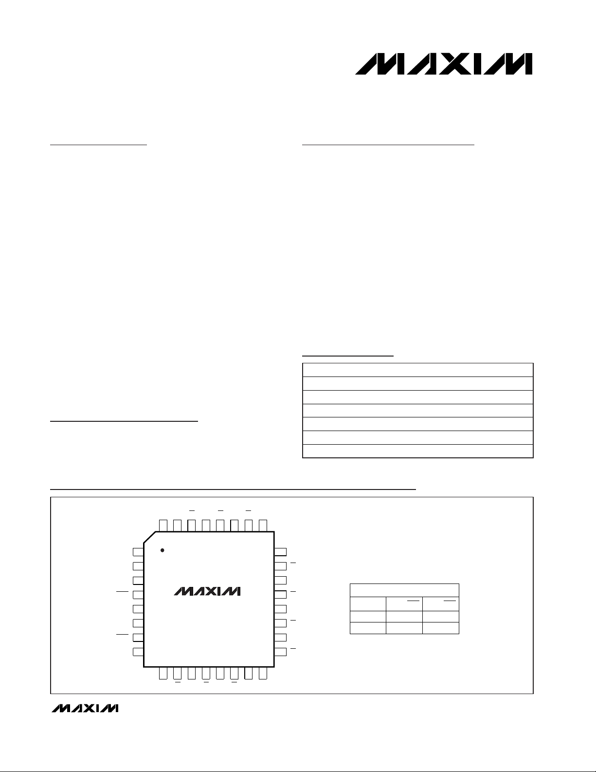
TOP VIEW
32 28293031 252627
V
CC
Q1Q0
V
CC
Q2
10
13
15
14
1611 12
9
17
18
19
20
21
22
23
24 Q3
Q4
Q5
Q6
V
EE
V
BB
CLK0
CLKSEL
2
3
4
5
6
7
8
1V
CC
MAX9311
MAX9313
Q0
Q1
Q2
Q3
Q4
Q5
Q6
V
CC
Q8Q9
V
CC
Q7
Q9
Q8
Q7
CLK1
CLK1
CLK0
LQFP (7mm × 7mm), TQFP (5mm × 5mm),
QFN (NO LEADS EXTENDING FROM QFN PACKAGE)
CLKSEL
0
1
MAX9311/MAX9313
ON
OFF
OFF
ON
CLK0, CLK0 CLK1, CLK1
Pin Configuration
Ordering Information
19-2078; Rev 2; 10/02
PART
TEMP. RANGE
PIN-PACKAGE
MAX9311ECJ
32 LQFP (7mm ✕ 7mm)
MAX9311EGJ*
32 QFN (5mm ✕ 5mm)
MAX9311EHJ*
32 TQFP (5mm ✕ 5mm)
MAX9313ECJ
32 LQFP (7mm ✕ 7mm)
MAX9313EGJ*
32 QFN (5mm ✕ 5mm)
MAX9313EHJ*
32 TQFP (5mm ✕ 5mm)
For pricing, delivery, and ordering information, please contact Maxim/Dallas Direct! at
1-888-629-4642, or visit Maxim’s website at www.maxim-ic.com.
*Future product—contact factory for availability.
-40°C to +85°C
-40°C to +85°C
-40°C to +85°C
-40°C to +85°C
-40°C to +85°C
-40°C to +85°C
Page 2
MAX9311/MAX9313
1:10 Differential LVPECL/LVECL/HSTL
Clock and Data Drivers
2 _______________________________________________________________________________________
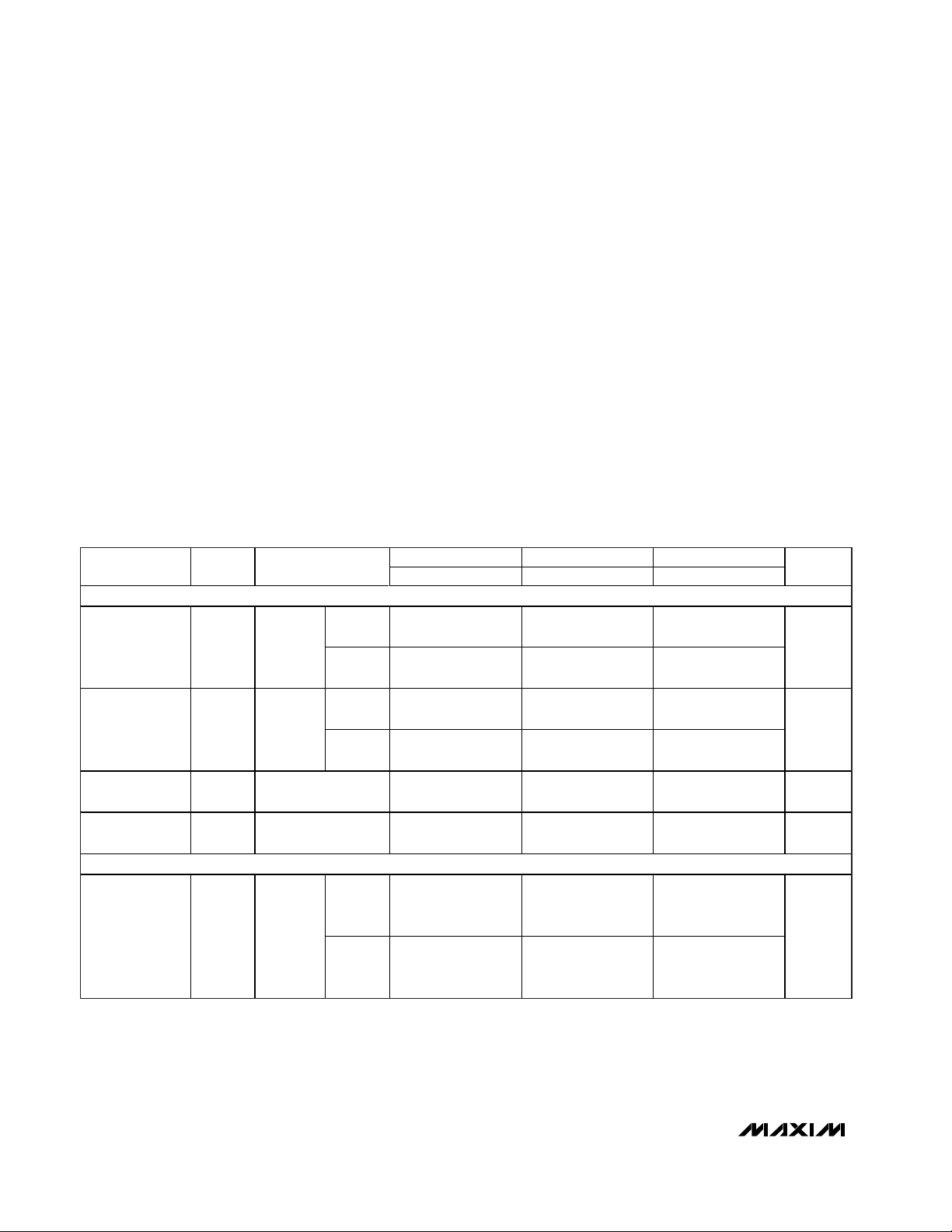
ABSOLUTE MAXIMUM RATINGS
DC ELECTRICAL CHARACTERISTICS
(VCC- VEE= +2.25V to +3.8V, outputs loaded with 50Ω ±1% to VCC- 2V, CLKSEL = high or low, unless otherwise noted.) (Notes 1–4)
Stresses beyond those listed under “Absolute Maximum Ratings” may cause permanent damage to the device. These are stress ratings only, and functional
operation of the device at these or any other conditions beyond those indicated in the operational sections of the specifications is not implied. Exposure to
absolute maximum rating conditions for extended periods may affect device reliability.
VCC- VEE...............................................................................4.1V
Inputs (CLK_,
CLK_, CLKSEL)..............VEE- 0.3V to VCC+ 0.3V
CLK_ to CLK_ ....................................................................±3.0V
Continuous Output Current .................................................50mA
Surge Output Current........................................................100mA
V
BB
Sink/Source Current ...............................................±0.65mA
Junction-to-Ambient Thermal Resistance in Still Air
7mm x 7mm LQFP .....................................................+90°C/W
Junction-to-Ambient Thermal Resistance with
500 LFPM Airflow
7mm x 7mm LQFP .....................................................+60°C/W
Junction-to-Case Thermal Resistance
7mm x 7mm LQFP .....................................................+12°C/W
Operating Temperature Range ...........................-40°C to +85°C
Junction Temperature......................................................+150°C
Storage Temperature Range .............................-65°C to +150°C
ESD Protection
Human Body Model (CLKSEL, CLK_, CLK_,
Q_, Q_, V
BB
).......................................................................2kV
Soldering Temperature (10s) ...........................................+300°C
-40°C +25°C +85°C
PARAMETER
CONDITIONS
MIN MAX MIN MAX MIN MAX
UNITS
SINGLE-ENDED INPUT (CLKSEL)
V
CC
V
CC
V
CC
V
CC
V
CC
V
CC
Input High
Voltage
V
IH
Inter nal
V
B B
V
CC
V
CC
V
CC
V
CC
V
CC
V
CC
V
V
EE
V
CC
- 1.62
V
EE
V
CC
- 1.62
V
EE
V
CC
- 1.62
Input Low
Voltage
V
IL
Inter nal
V
B B
V
EE
V
CC
V
EE
V
CC
V
EE
V
CC
V
Input High
Current
I
IH
150 150 150 µA
Input Low
Current
I
IL
-10 +10 -10 +10 -10 +10 µA
DIFFERENTIAL INPUTS (CLK_, CLK_)
V
CC
V
CC
V
CC
V
CC
V
CC
V
CC
Single-Ended
Input High
Voltage
V
IH
V
BB
connected
to CLK _
( V
IL
for V
BB
connected
to C LK_) ,
Figure 1
V
CC
V
CC
V
CC
V
CC
V
CC
V
CC
V
SYMBOL
thr eshol d
M AX 9311
M AX 9313
- 1.23
- 1.165
- 1.23
- 1.165
M AX 9311
thr eshol d
M AX 9313
- 1.475
M AX 9311
M AX 9313
- 1.23
- 1.165
- 1.23
- 1.165
- 1.475
- 1.23
- 1.165
- 1.23
- 1.165
- 1.475
Page 3
MAX9311/MAX9313
1:10 Differential LVPECL/LVECL/HSTL
Clock and Data Drivers
_______________________________________________________________________________________ 3
DC ELECTRICAL CHARACTERISTICS (continued)
(VCC- VEE= +2.25V to +3.8V, outputs loaded with 50Ω ±1% to VCC- 2V, CLKSEL = high or low, unless otherwise noted.) (Notes 1–4)
-40°C +25°C +85°C
PARAMETER
CONDITIONS
MIN MAX MIN MAX MIN MAX
UNITS
V
EE
V
CC
- 1.62
V
EE
V
CC
- 1.62
V
EE
V
CC
-1.62
Single-Ended
Input Low
Voltage
V
IL
V
BB
connected
to CLK _
( V
IH
for V
BB
connected
to C LK_) ,
Figure 1
V
EE
V
CC
V
EE
V
CC
V
EE
V
CC
V
High Voltage
of Differential
Input
V
IHD
V
CC
V
CC
V
CC
V
Low Voltage
of Differential
Input
V
ILD
V
EE
V
CC
V
EE
V
CC
V
EE
V
CC
V
0.095
V
CC
- V
EE
0.095
V
CC
- V
EE
V
CC
- V
EE
Differential
Input Voltage
V
ILD
0.095 3.0 0.095 3.0
3.0
V
Input High
Current
I
IH
150 150 150 µA
CLK_ Input Low
Current
-10 +10 -10 +10 -10 +10 µA
CLK_ Input Low
Current
-150 -150 -150 µA
OUTPUTS (Q_, Q_)
Single-Ended
Output High
Voltage
V
OH
Figure 1
V
CC
V
CC
V
CC
V
CC
V
CC
V
CC
V
Single-Ended
Output Low
Voltage
V
OL
Figure 1
V
CC
V
CC
V
CC
V
CC
V
CC
V
CC
V
Differential
Output Voltage
V
OH
-
V
OL
Figure 1 670 950 670 950 670 950 mV
REFERENCE (VBB)
V
C C
V
C C
V
C C
V
C C
V
C C
V
C C
Reference
Voltage Output
(Note 5)
V
BB
IBB =
±0.5mA
V
CC
V
CC
- 1.26
V
CC
V
CC
- 1.26
V
CC
V
CC
- 1.26
V
POWER SUPPLY
Supply Current
(Note 6)
I
EE
75 82 95 mA
SYMBOL
M AX 9311
M AX 9313
V
I
ILCLK
I
ILCLK
For VCC - VEE < 3.0V
IHD -
For VCC - VEE ≥ 3.0V
VEE +1.2
- 1.475
- 0.095
VEE + 1.2
- 1.475
- 0.095
VEE +1.2
0.095
0.095
-1.475
- 0.095
- 1.025
- 0.900
- 1.025
- 0.900
- 1.025
- 0.900
M AX 9311
M AX 9313
- 1.93
- 1.525
- 1.38
- 1.695
- 1.325
- 1.93
- 1.525
- 1.38
- 1.695
- 1.325
- 1.93
- 1.525
- 1.38
- 1.695
- 1.325
Page 4
MAX9311/MAX9313
1:10 Differential LVPECL/LVECL/HSTL
Clock and Data Drivers
4 _______________________________________________________________________________________
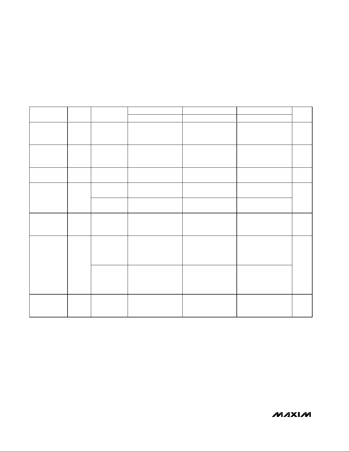
AC ELECTRICAL CHARACTERISTICS
(VCC- VEE= 2.25V to 3.8V, outputs loaded with 50Ω ±1% to VCC- 2V, input frequency = 1.5GHz, input transition time = 125ps
(20% to 80%), CLKSEL = high or low, V
IHD
= VEE+ 1.2V to VCC, V
ILD
= VEEto VCC- 0.15V, V
IHD
- V
ILD
= 0.15V to the smaller of 3V or
V
CC
- VEE, unless otherwise noted. Typical values are at VCC- VEE= 3.3V, V
IHD
= VCC-1V, V
ILD
= VCC-1.5V.) (Note 7)
-40°C +25°C +85°C
PARAMETER
SYMBOL
CONDITIONS
MA
UNITS
Differential
Input-toOutput Delay
t
PLHD
,
Figure 2
ps
Output-toOutput Skew
(Note 8)
12 46 12 46 10 35 ps
Part-to-Part
Skew (Note 9)
30
30
30
ps
f
IN
= 1.5GH z,
1.2
Added
Random Jitter
(Note 10)
t
RJ
f
IN
= 3.0GH z,
C l ock p atter n
ps
(RMS)
Added
Deterministic
Jitter (Note 10)
t
DJ
3Gbps,
2
23
-1 PRBS
pattern
80 95 80 95 80 95
ps
(p-p)
VOH - VOL ≥
350mV, Clock
pattern,
Figure 2
Switching
Frequency
f
MAX
VOH - VOL ≥
500mV, Clock
pattern,
Figure 2
GHz
Output
Rise/Fall Time
(20% to 80%)
Figure 2
ps
Note 1: Measurements are made with the device in thermal equilibrium.
Note 2: Current into a pin is defined as positive. Current out of a pin is defined as negative.
Note 3: Single-ended input operation using V
BB
is limited to VCC- VEE= 3.0V to 3.8V for the MAX9311 and VCC- VEE= 2.7V to 3.8V
for the MAX9313.
Note 4: DC parameters production tested at T
A
= +25°C. Guaranteed by design and characterization over the full operating temper-
ature range.
Note 5: Use V
BB
only for inputs that are on the same device as the VBBreference.
Note 6: All pins open except V
CC
and VEE.
Note 7: Guaranteed by design and characterization. Limits are set at ±6 sigma.
Note 8: Measured between outputs of the same part at the signal crossing points for a same-edge transition.
Note 9: Measured between outputs of different parts at the signal crossing points under identical conditions for a same-edge
transition.
Note 10:Device jitter added to the input signal.
t
PHLD
t
SKOO
t
SKPP
tR, t
C l ock p atter n
F
MIN TYP MAX MIN TYP
220 321 380 220 312 410 260 322 400
160
1.2 2.5 1.2 2.5
1.2 2.6 1.2 2.6 1.2 2.6
2.0 2.0 3.0 2.0
1.5 1.5 1.5
100 112 140 100 116 140 100 121 140
190
MIN TYP MAX
140
2.5
Page 5

MAX9311/MAX9313
1:10 Differential LVPECL/LVECL/HSTL
Clock and Data Drivers
_______________________________________________________________________________________ 5
Typical Operating Characteristics
(VCC= +3.3V, VEE= 0, V
IHD
= VCC- 0.95V, V
ILD
= VCC- 1.25V, input transition time = 125ps (20% to 80%), fIN= 1.5GHz, outputs
loaded with 50Ω to VCC- 2V, TA= +25°C, unless otherwise noted.)
50
60
55
70
65
80
75
85
-40 10-15 35 60 85
SUPPLY CURRENT (IEE)
vs. TEMPERATURE
MAX9311 toc01
TEMPERATURE (°C)
SUPPLY CURRENT (mA)
0
0.2
0.3
0.4
0.5
0.6
0.7
0.8
0.9
0 1000 2000 3000
OUTPUT AMPLITUDE (V
OH
- VOL)
vs. FREQUENCY
MAX9311 toc02
FREQUENCY (MHz)
OUTPUT AMPLITUDE (V)
0.1
100
130
-40 -15 10 35 60 85
TRANSITION TIME vs. TEMPERATURE
MAX9311 toc03
TEMPERATURE (°C)
TRANSITION TIME (ps)
105
110
115
120
125
t
R
t
F
303
305
304
307
306
309
308
310
312
311
313
1.0 3.8
PROPAGATION DELAY
vs. HIGH VOLTAGE OF
DIFFERENTIAL INPUT (V
IHD
)
MAX9311 toc04
V
IHD
(V)
PROPAGATION DELAY (ps)
1.4 1.8 2.2 3.43.02.6
t
PLHD
t
PHLD
V
IHD - VILD
= 150mV
200
220
240
260
280
300
320
340
360
-40 -15 10 35 60 85
PROPAGATION DELAY
vs. TEMPERATURE
MAX9311 toc05
TEMPERATURE (°C)
PROPAGATION DELAY (ps)
V
IHD
= V
CC
- 0.95V
V
ILD
= V
CC
- 1.1V
t
PLHD
t
PHLD
Page 6

MAX9311/MAX9313
1:10 Differential LVPECL/LVECL/HSTL
Clock and Data Drivers
6 _______________________________________________________________________________________
Pin Description
PIN NAME FUNCTION
1, 9, 16,
25, 32
V
CC
Positive Supply Voltage. Bypass from VCC to VEE with 0.1µF and 0.01µF ceramic capacitors. Place the
capacitors as close to the device as possible with the smaller value capacitor closest to the device.
2
Clock Select Input (Single-Ended). Drive low to select the CLK0, CLK0 input. Drive high to select the
CLK1, CLK1 input. The CLKSEL threshold is V
BB
. If CLKSEL is not driven by a logic signal, use a 1kΩ
pulldown to V
EE
to select CLK0, CLK0, or a 1kΩ pullup to VCC to select CLK1, CLK1.
3 CLK0 Noninverting Differential Clock Input 0. Internal 75kΩ pulldown resistor.
4 CLK0 Inverting Differential Clock Input 0. Internal 75kΩ pullup and pulldown resistors.
5V
BB
Refer ence Outp ut V ol tag e. C onnect to the i nver ti ng or noni nver ti ng cl ock i np ut to p r ovi d e a r efer ence for
si ng l e- end ed op er ati on. W hen used , b yp ass w i th a 0.01µF cer am i c cap aci tor to V
C C
; other w i se, l eave op en.
6 CLK1 Noninverting Differential Clock Input 1. Internal 75kΩ pulldown resistor.
7 CLK1 Inverting Differential Clock Input 1. Internal 75kΩ pullup and pulldown resistors.
8VEENegative Supply Voltage
10 Q9 Inverting Q9 Output. Typically terminate with 50Ω resistor to VCC - 2V.
11 Q9 Noninverting Q9 Output. Typically terminate with 50Ω resistor to VCC - 2V.
12 Q8 Inverting Q8 Output. Typically terminate with 50Ω resistor to VCC - 2V.
13 Q8 Noninverting Q8 Output. Typically terminate with 50Ω resistor to VCC - 2V.
14 Q7 Inverting Q7 Output. Typically terminate with 50Ω resistor to VCC - 2V.
15 Q7 Noninverting Q7 Output. Typically terminate with 50Ω resistor to VCC - 2V.
17 Q6 Inverting Q6 Output. Typically terminate with 50Ω resistor to VCC - 2V.
18 Q6 Noninverting Q6 Output. Typically terminate with 50Ω resistor to VCC - 2V.
19 Q5 Inverting Q5 Output. Typically terminate with 50Ω resistor to VCC - 2V.
20 Q5 Noninverting Q5 Output. Typically terminate with 50Ω resistor to VCC - 2V.
21 Q4 Inverting Q4 Output. Typically terminate with 50Ω resistor to VCC - 2V.
22 Q4 Noninverting Q4 Output. Typically terminate with 50Ω resistor to VCC - 2V.
23 Q3 Inverting Q3 Output. Typically terminate with 50Ω resistor to VCC - 2V.
24 Q3 Noninverting Q3 Output. Typically terminate with 50Ω resistor to VCC - 2V.
26 Q2 Inverting Q2 Output. Typically terminate with 50Ω resistor to VCC - 2V.
27 Q2 Noninverting Q2 Output. Typically terminate with 50Ω resistor to VCC - 2V.
28 Q1 Inverting Q1 Output. Typically terminate with 50Ω resistor to VCC - 2V.
29 Q1 Noninverting Q1 Output. Typically terminate with 50Ω resistor to VCC - 2V.
30 Q0 Inverting Q0 Output. Typically terminate with 50Ω resistor to VCC - 2V.
31 Q0 Noninverting Q0 Output. Typically terminate with 50Ω resistor to VCC - 2V.
CLKSEL
Page 7

MAX9311/MAX9313
1:10 Differential LVPECL/LVECL/HSTL
Clock and Data Drivers
_______________________________________________________________________________________ 7
Detailed Description
The MAX9311/MAX9313 are low skew, 1-to-10 differential drivers designed for clock and data distribution.
A 2:1 mux selects between the two differential inputs,
CLK0, CLK0 and CLK1, CLK1. The 2:1 mux is switched
by the single-ended CLKSEL input. A logic low selects
the CLK0, CLK0 input. A logic high selects the CLK1,
CLK1 input. The logic threshold for CLKSEL is set by an
internal VBBvoltage reference. The CLKSEL input can
be driven to VCCand VEEor by a single-ended LVPECL/
LVECL signal. The selected input is reproduced at 10
differential outputs.
For interfacing to differential HSTL and LVPECL signals,
these devices operate over a +2.25V to +3.8V supply
range, allowing high-performance clock or data distribution in systems with a nominal +2.5V or +3.3V supply.
For differential LVECL operation, these devices operate
from a -2.25V to -3.8V supply.
The differential inputs can be configured to accept single-ended inputs when operating at approximately VCCVEE= +3.0V to +3.8V for the MAX9311 or VCC- VEE=
+2.7V to +3.8V for the MAX9313. This is accomplished
by connecting the on-chip reference voltage, VBB, to an
input as a reference. For example, the differential CLK0,
CLK0 input is converted to a noninverting, single-ended
input by connecting VBBto CLK0 and connecting the
single-ended input to CLK0. Similarly, an inverting input
is obtained by connecting VBBto CLK0 and connecting
the single-ended input to CLK0. With a differential input
configured as single-ended (using VBB), the singleended input can be driven to VCCand VEEor with a single-ended LVPECL/LVECL signal.
When a differential input is configured as a single-ended
input (using VBB), the approximate supply range is VCCVEE= +3.0V to +3.8V for the MAX9311 and VCC- VEE=
+2.7V to +3.8V for the MAX9313. This is because one of
the inputs must be VEE+ 1.2V or higher for proper operation of the input stage. VBBmust be at least VEE+ 1.2V
because it becomes the high-level input when the other
(single-ended) input swings below it. Therefore, minimum VBB= VEE+ 1.2V.
The minimum V
BB
output for the MAX9311 is VCC-
1.525V and the minimum VBBoutput for the MAX9313 is
VCC- 1.38V. Substituting the minimum VBBoutput for
each device into VBB= VEE+ 1.2V results in a minimum
supply of 2.725V for the MAX9311 and 2.58V for the
MAX9313. Rounding up to standard supplies gives the
single-ended operating supply ranges of VCC- VEE=
3.0V to 3.8V for the MAX9311 and VCC- VEE= 2.7V to
3.8V for the MAX9313.
When using the V
BB
reference output, bypass it with a
0.01µF ceramic capacitor to VCC. If the VBBreference is
not used, it can be left open. The VBBreference can
source or sink 0.5mA, which is sufficient to drive two
inputs. Use VBBonly for inputs that are on the same
device as the VBBreference.
The maximum magnitude of the differential input from
CLK_ to CLK_ is 3.0V or VCC- VEE, whichever is less.
This limit also applies to the difference between any reference voltage input and a single-ended input.
The differential inputs have bias resistors that drive the
outputs to a differential low when the inputs are open.
The inverting inputs (CLK0 and CLK1) are biased with a
75kΩ pullup to VCCand a 75kΩ pulldown to VEE. The
noninverting inputs (CLK0 and CLK1) are biased with a
75kΩ pulldown to V
EE
. The single-ended CLKSEL input
does not have a bias resistor. If not driven, pull CLKSEL
up or down with a 1kHz resistor (see Pin Description).
Specifications for the high and low voltages of a differential input (V
IHD
and V
ILD
) and the differential input volt-
age (V
IHD
- V
ILD
) apply simultaneously (V
ILD
cannot be
higher than V
IHD
).
Output levels are referenced to VCCand are considered
LVPECL or LVECL, depending on the level of the V
CC
supply. With VCCconnected to a positive supply and
V
EE
connected to GND, the outputs are LVPECL. The
outputs are LVECL when VCCis connected to GND and
V
EE
is connected to a negative supply.
A single-ended input of at least VBB±95mV or a differential input of at least 95mV switches the outputs to the
V
OH
and VOLlevels specified in the DC Electrical
Characteristics table.
Applications Information
Supply Bypassing
Bypass VCCto VEEwith high-frequency surface-mount
ceramic 0.1µF and 0.01µF capacitors in parallel as close
to the device as possible, with the 0.01µF value capacitor closest to the device. Use multiple parallel vias for
low inductance. When using the VBBreference output,
bypass it with a 0.01µF ceramic capacitor to VCC(if the
VBBreference is not used, it can be left open).
Traces
Input and output trace characteristics affect the performance of the MAX9311/MAX9313. Connect each signal
of a differential input or output to a 50Ω characteristic
impedance trace. Minimize the number of vias to prevent
impedance discontinuities. Reduce reflections by maintaining the 50Ω characteristic impedance through connectors and across cables. Reduce skew within a
Page 8

MAX9311/MAX9313
1:10 Differential LVPECL/LVECL/HSTL
Clock and Data Drivers
8 _______________________________________________________________________________________
differential pair by matching the electrical length of the
traces.
Output Termination
Terminate outputs through 50Ω to VCC- 2V or use an
equivalent Thevenin termination. When a single-ended
signal is taken from a differential output, terminate both
outputs. For example, if Q0 is used as a single-ended
output, terminate both Q0 and Q0.
Chip Information
TRANSISTOR COUNT: 250
V
IL
V
IH
V
OH -
V
OL
V
OH
V
OL
Q_
Q_
CLK_
CLK_
(CONNECTED TO CLK_)
V
BB
Figure 1. Switching with Single-Ended Input
0 (DIFFERENTIAL)
80%
20%
80%
20%
0 (DIFFERENTIAL)
VOH - V
OL
V
IHD
- V
ILD
V
IHD
V
ILD
Q_
Q_
(Q_) - (Q_)
CLK_
CLK_
t
PLHD
t
PHLD
t
R
t
F
V
OH
V
OL
Figure 2. Differential Transition Time and Propagation Delay Timing Diagram
Page 9

MAX9311/MAX9313
1:10 Differential LVPECL/LVECL/HSTL
Clock and Data Drivers
_______________________________________________________________________________________ 9
Q0
CLK0
0
1
V
CC
75kΩ
75kΩ 75kΩ
Q0
Q2
Q2
Q3
Q3
Q4
Q4
Q5
Q5
Q6
Q6
Q7
Q7
Q8
Q8
Q9
Q9
Q1
Q1
CLK0
CLK1
CLKSEL
V
CC
75kΩ
75kΩ 75kΩ
CLK1
V
EE
V
EE
V
EE
V
EE
V
BB
Functional Diagram
Page 10

MAX9311/MAX9313
1:10 Differential LVPECL/LVECL/HSTL
Clock and Data Drivers
10 ______________________________________________________________________________________
32L/48L TQFP EPS
Package Information
(The package drawing(s) in this data sheet may not reflect the most current specifications. For the latest package outline information
go to www.maxim-ic.com/packages.)
Page 11

MAX9311/MAX9313
1:10 Differential LVPECL/LVECL/HSTL
Clock and Data Drivers
______________________________________________________________________________________ 11
32L TQFP, 5x5x01.0.EPS
Package Information (continued)
(The package drawing(s) in this data sheet may not reflect the most current specifications. For the latest package outline information
go to www.maxim-ic.com/packages.)
Page 12

MAX9311/MAX9313
1:10 Differential LVPECL/LVECL/HSTL
Clock and Data Drivers
Maxim cannot assume responsibility for use of any circuitry other than circuitry entirely embodied in a Maxim product. No circuit patent licenses are
implied. Maxim reserves the right to change the circuitry and specifications without notice at any time.
12 ____________________Maxim Integrated Products, 120 San Gabriel Drive, Sunnyvale, CA 94086 408-737-7600
© 2002 Maxim Integrated Products Printed USA is a registered trademark of Maxim Integrated Products.
32L QFN.EPS
Package Information (continued)
(The package drawing(s) in this data sheet may not reflect the most current specifications. For the latest package outline information
go to www.maxim-ic.com/packages.)
 Loading...