

Page 1
General Description
The MAX9310A is a fast, low-skew 1:5 differential driver
with selectable LVPECL inputs and LVDS outputs,
designed for clock distribution applications. This device
features an ultra-low propagation delay of 340ps with
48mA of supply current.
The MAX9310A operates from a 3V to 3.6V power supply for use in 3.3V systems. A 2:1 input multiplexer is
used to select one of two differential inputs. The input
selection is controlled through the CLKSEL pin.
This device features a synchronous enable function.
The MAX9310A LVPECL inputs can be driven by either
a differential or single-ended signal. A VBBreference
voltage output is provided for use with single-ended
inputs. The device can also accept differential HSTL
signals.
The MAX9310A is offered in a space-saving 20-pin
TSSOP package and operates over the extended temperature range from -40°C to +85°C.
Applications
Data and Clock Drivers and Buffers
Central-Office Backplane Clock Distribution
DSLAM
Base Stations
ATE
Features
♦ Guaranteed 1.0GHz Operating Frequency
♦ 8.0ps Output-to-Output Skew
♦ 340ps Propagation Delay
♦ Accepts LVPECL and Differential HSTL Inputs
♦ Synchronous Output Enable/Disable
♦ Two Selectable Differential Inputs
♦ 3V to 3.6V Supply Voltage
♦ On-Chip Reference for Single-Ended Operation
♦ ESD Protection: ±2kV (Human Body Model)
♦ Input Bias Resistors Drive Output Low for Open
Inputs
MAX9310A
1:5 Clock Driver with Selectable LVPECL
Inputs/Single-Ended Inputs and LVDS Outputs
________________________________________________________________ Maxim Integrated Products 1
20
19
18
17
16
15
14
13
1
2
3
4
5
6
7
8
V
CC
EN
V
CC
CLK1Q1
Q1
QO
Q0
TOP VIEW
CLK1
V
BB
CLK0
CLK0Q3
Q3
Q2
Q2
12
11
9
10
CLKSEL
GNDQ4
Q4
MAX9310A
TSSOP
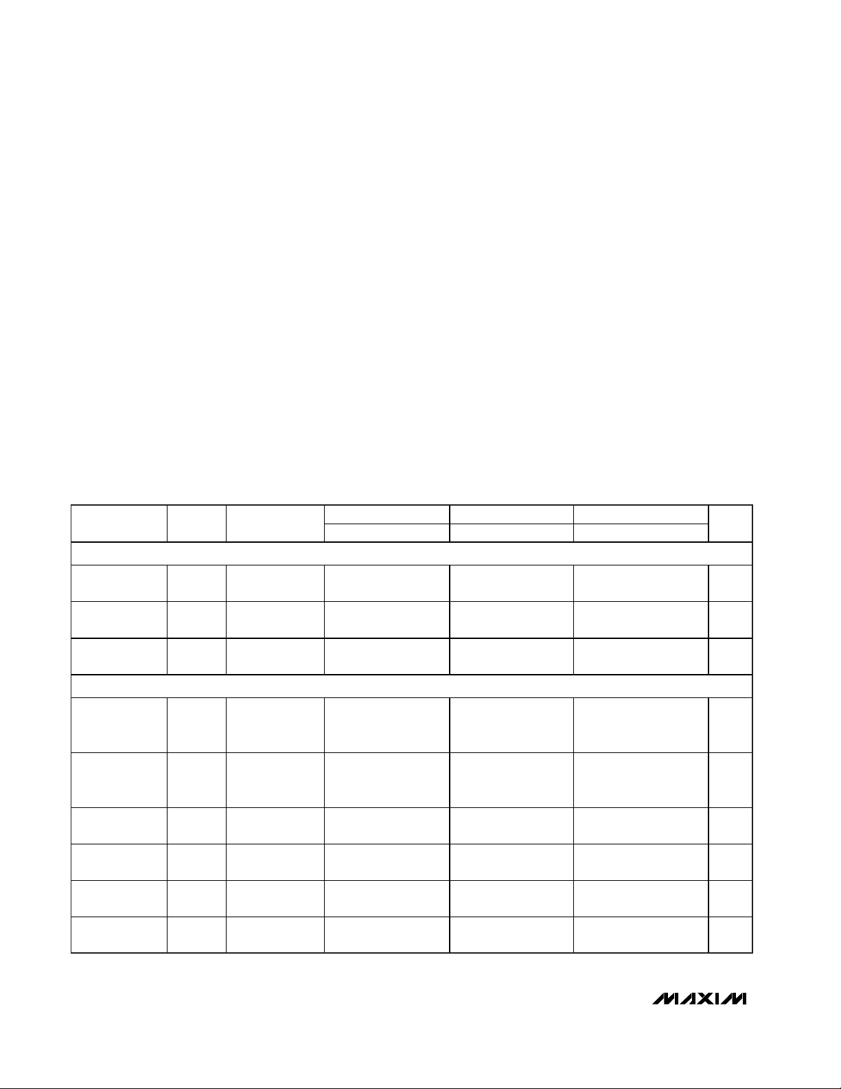
Pin Configuration
Ordering Information
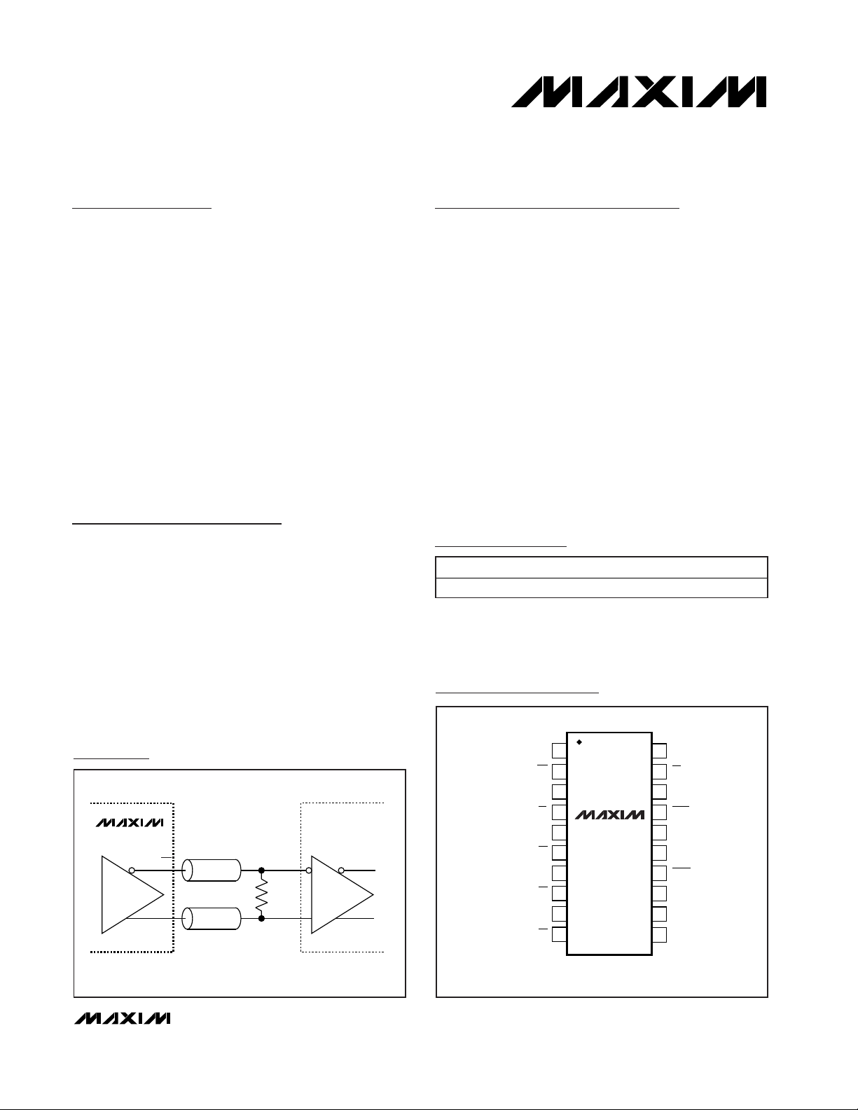
100Ω
MAX9310A
ZO = 50Ω
Z
O
= 50Ω
RECEIVER
Q_
Q_
Typical Application Circuit
19-2542; Rev 0; 7/02
For pricing, delivery, and ordering information, please contact Maxim/Dallas Direct! at
1-888-629-4642, or visit Maxim’s website at www.maxim-ic.com.
Functional Diagram appears at end of data sheet.
PART TEMP RANGE PIN-PACKAGE
MAX9310AEUP
-40°C to +85°C 20 TSSOP
Page 2
MAX9310A
1:5 Clock Driver with Selectable LVPECL
Inputs/Single-Ended Inputs and LVDS Outputs
2 _______________________________________________________________________________________
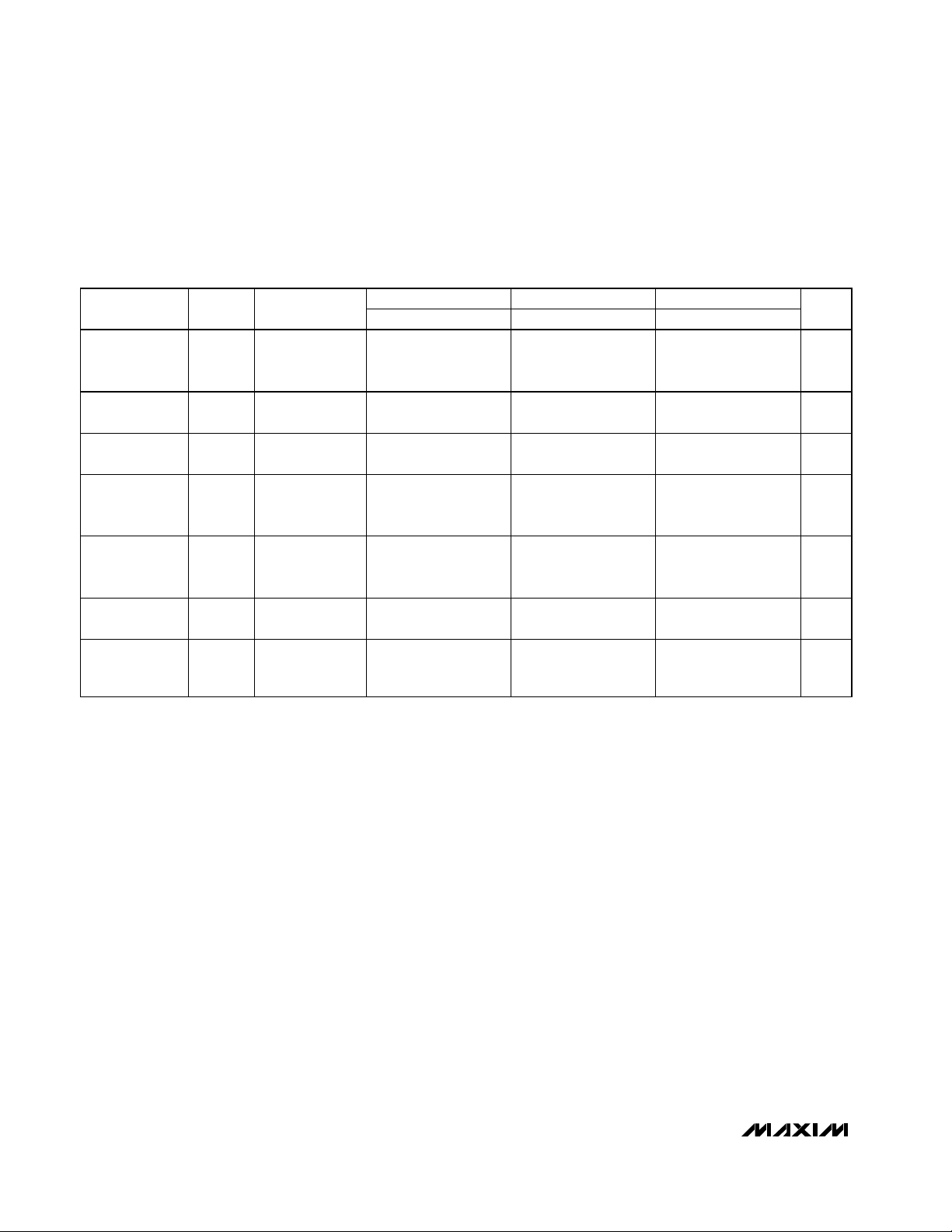
ABSOLUTE MAXIMUM RATINGS
DC ELECTRICAL CHARACTERISTICS
(VCC- GND = 3V to 3.6V, outputs terminated with 100Ω±1%, unless otherwise noted. Typical values are at VCC- GND = 3.3V, V
IHD
=
V
CC
- 1.0V, V
ILD
= VCC- 1.5V, unless otherwise noted.) (Notes 1, 2, and 3)
Stresses beyond those listed under “Absolute Maximum Ratings” may cause permanent damage to the device. These are stress ratings only, and functional
operation of the device at these or any other conditions beyond those indicated in the operational sections of the specifications is not implied. Exposure to
absolute maximum rating conditions for extended periods may affect device reliability.
VCCto GND...........................................................-0.3V to +4.1V
EN, CLKSEL, CLK_, CLK_, to GND............-0.3V to (VCC+ 0.3V)
CLK_ to CLK_.........................................................................±3V
Continuous Output Current .................................................24mA
Surge Output Current..........................................................50mA
V
BB
Sink/Source Current ...............................................±0.65mA
Continuous Power Dissipation (T
A
= +70°C)
Single-Layer PC Board
20-Pin TSSOP (derate 7.69mW/°C above +70°C) ......615mW
Multilayer PC Board
20-Pin TSSOP (derate 11mW/°C above +70°C) .........879mW
Junction-to-Ambient Thermal Resistance in Still Air
Single-Layer PC Board
20-Pin TSSOP .........................................................+130°C/W
Multilayer PC Board
20-Pin TSSOP ...........................................................+91°C/W
Junction-to-Ambient Thermal Resistance with 500LFPM
Airflow Single-Layer PC board
20-Pin TSSOP ...........................................................+96°C/W
Junction-to-Case Thermal Resistance
20-Pin TSSOP ...........................................................+20°C/W
Operating Temperature Range .......................... -40°C to +85°C
Junction Temperature......................................................+150°C
Storage Temperature Range .............................-65°C to +150°C
ESD Protection
Human Body Model (inputs and outputs) .......................±2kV
Lead Temperature (soldering, 10s) .................................+300°C
-40°C +25°C +85°C
PARAMETER
SYMBOL
CONDITIONS
UNITS
SINGLE-ENDED INPUTS (CLKSEL, EN)
Input High
Voltage
V
IH
VCC -
VCC -
VCC -
VCC -
VCC -
VCC -
V
Input Low
Voltage
V
IL
VCC -
VCC -
VCC -
VCC -
VCC -
VCC -
V
Input Current I
IN
V
IH(MAX)
,
V
IL(MAX)
µA
DIFFERENTIAL INPUTS (CLK_, CLK_)
Single-Ended
Input High
Voltage
V
IH
Figure 1
V
CC
-
VCC -
VCC -
VCC -
VCC -
VCC -
V
Single-Ended
Input Low
Voltage
V
IL
Figure 1
V
CC
-
VCC -
VCC -
VCC -
VCC -
VCC -
V
Differential Input
High Voltage
V
IHD
Figure 2
V
Differential Input
Low Voltage
V
ILD
Figure 2
VCC -
VCC -
VCC -
V
Differential Input
Voltage
V
ID
V
IHD
- V
ILD
3.0 V
Input Current
CLK_, or CLK_ =
V
IHD
or V
ILD
µA
MIN TYP MAX MIN TYP MAX MIN TYP MAX
IIH, I
IL
1.165
1.81
-10 +70 -10 +70 -10 +70
1.125
1.81
1.2 V
GND
0.095 3.0 0.095 3.0 0.095
-100 +100 -100 +100 -100 +100
0.88
1.475
0.88
1.475
CC
0.095
1.165
1.81
1.165
1.81
1.2 V
GND
0.88
1.475
0.88
1.475
CC
0.095
1.165
1.81
1.165
1.81
1.2 V
GND
0.88
1.475
0.88
1.495
CC
0.095
Page 3

MAX9310A
1:5 Clock Driver with Selectable LVPECL
Inputs/Single-Ended Inputs and LVDS Outputs
_______________________________________________________________________________________ 3
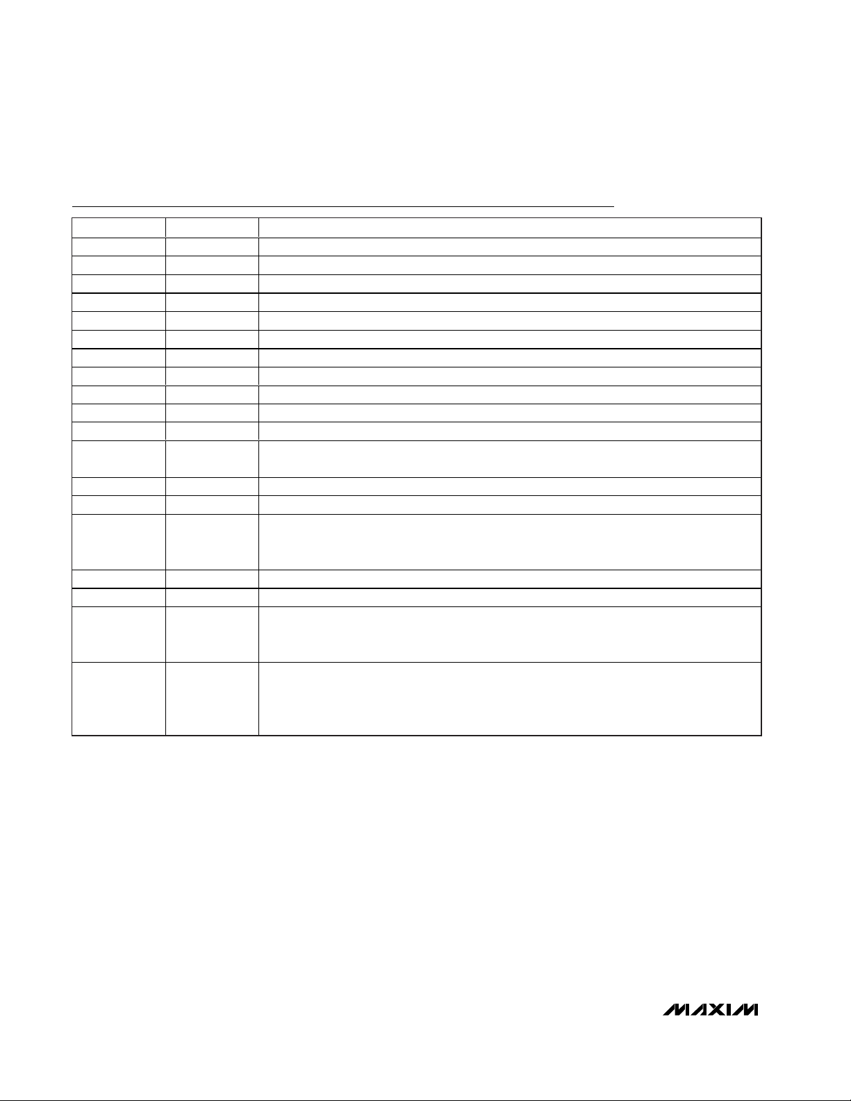
DC ELECTRICAL CHARACTERISTICS (continued)
(VCC- GND = 3V to 3.6V, outputs terminated with 100Ω±1%, unless otherwise noted. Typical values are at VCC- GND = 3.3V, V
IHD
=
V
CC
- 1.0V, V
ILD
= VCC- 1.5V, unless otherwise noted.) (Notes 1, 2, and 3)
-40°C +25°C +85°C
PARAMETER
SYMBOL
CONDITIONS
UNITS
OUTPUTS (Q_, Q_)
Output High
Voltage
V
OH
Figure 2
1.6 V
Output Low
Voltage
V
OL
Figure 2
V
Differential
Output Voltage
V
OD
VOH - VOL,
Figure 2
mV
Change in V
OD
Between
Complementary
Output States
∆V
OD
50 50 50
mV
Output Offset
Voltage
V
OS
mV
Change in VOS
Between
Complementary
Output States
25 25 25
mV
12 12 12
Output ShortCircuit Current
I
OSC
Q_ or Q_ shorted
to GND
29 29 29
mA
REFERENCE
Reference
Voltage Output
V
BB
IBB = ±0.65mA
(Note 4)
VCC -
VCC -
VCC -
VCC -
VCC -
VCC -
V
POWER SUPPLY
Power-Supply
Current
I
CC
(Note 5)
75
75 51 75
mA
MIN TYP MAX MIN TYP MAX MIN TYP MAX
0.9 0.9 0.9
250 350 450 250 350 450 250 350 450
1.125 1.25 1.375 1.125 1.25 1.375 1.125 1.25 1.375
∆VOCM
Q_ shorted to Q_
1.6 1.6
1.38
45
1.22
1.38
1.26
48
1.40
1.26
Page 4
MAX9310A
4 _______________________________________________________________________________________
Note 1: Measurements are made with the device in thermal equilibrium.
Note 2: Current into a pin is defined as positive. Current out of a pin is defined as negative.
Note 3: DC parameters are production tested at +25°C. DC limits are guaranteed by design and
characterized over the full operating temperature range.
Note 4: Use V
BB
only for inputs that are on the same device as the VBBreference.
Note 5: All pins are open except V
CC
and GND, all outputs are loaded with 100Ω differentially.
Note 6: Guaranteed by design and characterization. Limits are set to ±6 sigma.
Note 7: Measured between outputs of the same part at the signal crossing points for a same-edge
transition.
Note 8: Measured between outputs of different parts at the signal crossing points under identical conditions
for a same-edge transition.
Note 9: Device jitter added to the input signal.
AC ELECTRICAL CHARACTERISTICS
(VCC- GND = 3V to 3.6V, outputs terminated with 100Ω±1%, fIN≤ 1.0GHz, input transition time = 125ps (20% to 80%),
V
IHD
- V
ILD
= 0.15V to VCC, unless otherwise noted. Typical values are at VCC- GND = 3.3V, V
IHD
= VCC- 1.0V, V
ILD
= VCC- 1.5V,
unless otherwise noted.) (Notes 1 and 6)
-40°C +25°C +85°C
PARAMETER
SYMBOL
CONDITIONS
UNITS
Propagation
Delay CLK_,
CLK_ to Q_, Q_
t
PHL
,
t
PLH
Figure 2
ps
Output-toOutput Skew
(Note 7) 10 30 8 25 20 45 ps
Part-to-Part
Skew
t
SKPP
(Note 8)
ps
Added Random
Jitter
t
RJ
fIN = 1.0GHz,
clock pattern
(Note 9)
ps
(RMS)
Added
Deterministic
Jitter
t
DJ
fIN = 1.0Gsps,
2
23
- 1 PRBS
50 60 50 60 50 60
ps
(P-P)
Operating
Frequency
f
MAX
VOD ≥ 250mV
GHz
Differential
Output Rise/Fall
Time
t
R/tF
20% to 80%,
Figure 2
ps
1:5 Clock Driver with Selectable LVPECL
Inputs/Single-Ended Inputs and LVDS Outputs
MIN TYP MAX MIN TYP MAX MIN TYP MAX
250 340 600 250 340 600 250 340 600
t
SKOO
145 145 145
0.3 1.0 0.3 1.0 0.3 1.0
pattern (Note 9)
1.0 1.0 1.0
140 205 300 140 205 300 140 205 300
Page 5

MAX9310A
1:5 Clock Driver with Selectable LVPECL
Inputs/Single-Ended Inputs and LVDS Outputs
_______________________________________________________________________________________ 5
SUPPLY CURRENT vs. TEMPERATURE
MAX9310A toc01
TEMPERATURE (°C)
SUPPLY CURRENT (mA)
603510-15
43
44
45
46
47
48
49
50
51
52
42
-40 85
ALL PINS ARE OPEN EXCEPT VCC
AND GND OUTPUTS LOADED WITH 100Ω
DIFFERENTIAL
DIFFERENTIAL OUTPUT VOLTAGE (VOH - VOL)
vs. FREQUENCY
MAX9310A toc02
FREQUENCY (GHz)
DIFFERENTIAL OUTPUT VOLTAGE (mV)
1.501.250.25 0.50 0.75 1.00
100
150
200
250
300
350
400
450
50
0 1.75
OUTPUT RISE/FALL vs. TEMPERATURE
MAX9310A toc03
TEMPERATURE (°C)
RISE/FALL TIME (ps)
603510-15
205
210
215
220
200
-40 85
t
F
t
R
fIN = 500MHz
Typical Operating Characteristics
(VCC- GND = 3.3V, outputs terminated with 100Ω±1%, fIN= 1.0GHz, input transition time = 125ps (20% to 80%),V
IHD
= VCC- 1.0V,
V
ILD
= VCC- 1.5V, unless otherwise noted.)
PROPAGATION DELAY vs. HIGH VOLTAGE
OF DIFFERENTIAL INPUT (V
IHD
)
MAX9310A toc04
V
IHD
(V)
PROPAGATION DELAY (ps)
3.02.72.42.11.81.5
310
330
350
370
390
290
1.2 3.3
PROPAGATION DELAY vs. TEMPERATURE
MAX9310A toc05
TEMPERATURE (°C)
PROPAGATION DELAY (ps)
603510-15
320
340
360
380
400
300
-40 85
Page 6
MAX9310A
6 _______________________________________________________________________________________
Pin Description
PIN NAME FUNCTION
1 Q0 Noninverting Differential Output 0. Typically terminated with 100Ω to Q0.
2 Q0 Inverting Differential Output 0. Typically terminated with 100Ω to Q0.
3 Q1 Noninverting Differential Output 1. Typically terminated with 100Ω to Q1.
4 Q1 Inverting Differential Output 1. Typically terminated with 100Ω to Q1.
5 Q2 Noninverting Differential Output 2. Typically terminated with 100Ω to Q2.
6 Q2 Inverting Differential Output 2. Typically terminated with 100Ω to Q2.
7 Q3 Noninverting Differential Output 3. Typically terminated with 100Ω to Q3.
8 Q3 Inverting Differential Output 3. Typically terminated with 100Ω to Q3.
9 Q4 Noninverting Differential Output 4. Typically terminated with 100Ω to Q4.
10 Q4 Inverting Differential Output 4. Typically terminated with 100Ω to Q4.
11 GND Ground
12 CLKSEL
Clock Select Input. Drive low to select the CLK0, CLK0 input. Drive high to select the CLK1,
CLK1 input. The CLKSEL threshold is equal to V
BB
. Internal 60kΩ pulldown to GND.
13 CLK0 Noninverting Differential Clock Input 0. Internal 75kΩ pulldown to GND.
14 CLK0 Inverting Differential Clock Input 0. Internal 75kΩ pullup to VCC and 75kΩ pulldown to GND.
15 V
BB
Reference Output Voltage. Connect to the inverting or noninverting clock input to provide a
reference for single-ended operation. When used, bypass with a 0.01µF ceramic capacitor to
V
CC
; otherwise, leave open.
16 CLK1 Noninverting Differential Input 1. Internal 75kΩ pulldown to GND.
17 CLK1 Inverting Differential Input 1. Internal 75kΩ pullup to VCC and 75kΩ pulldown to GND.
18, 20 V
CC
Positive Supply Voltage. Bypass VCC to GND with 0.1µF and 0.01µF ceramic capacitors. Place
the capacitors as close to the device as possible with the smaller value capacitor closest to the
device.
19 EN
Output Enable Input. Outputs are synchronously enabled on the falling edge of the selected
clock input when EN is low. Outputs are synchronously driven to a differential low state on the
falling edge of the selected clock input when EN is high. Internal 60kΩ pulldown to GND
(Figure 3).
1:5 Clock Driver with Selectable LVPECL
Inputs/Single-Ended Inputs and LVDS Outputs
Page 7
MAX9310A
1:5 Clock Driver with Selectable LVPECL
Inputs/Single-Ended Inputs and LVDS Outputs
_______________________________________________________________________________________ 7
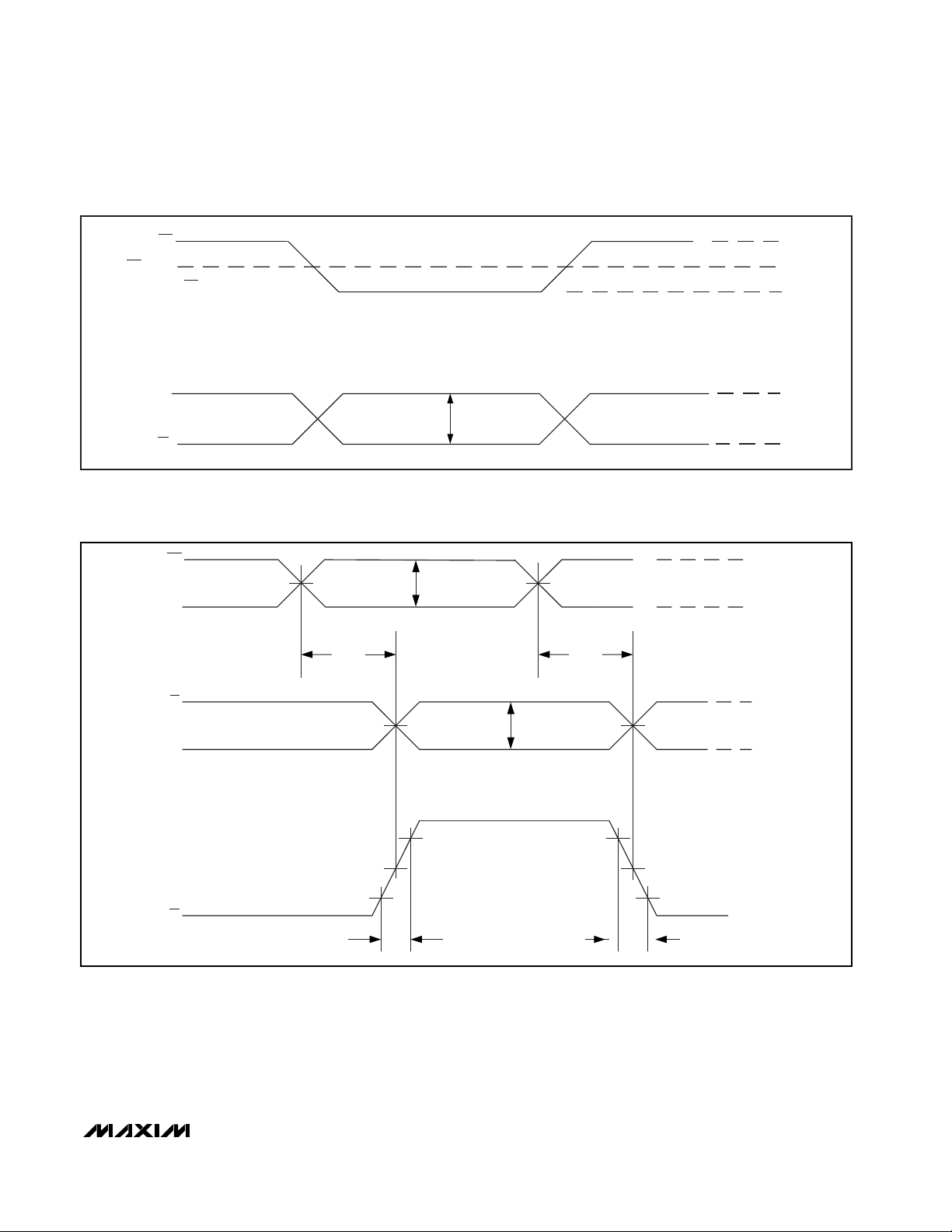
CLK
CLK
Q_
Q_
t
PLHD
t
PHLD
VOH - V
OL
V
IHD
- V
ILD
V
IHD
V
ILD
Q_ - Q_
0V (DIFFERENTIAL) 0V (DIFFERENTIAL)
20%
80%
20%
80%
t
R
t
F
V
OL
V
OH
Figure 2. MAX9310A Timing Diagram
Q_
V
OH
V
OL
V
IH
V
IL
V
BB
(CLK IS CONNECTED TO VBB)
VOH - V
OL
CLK OR CLK
Q_
CLK OR CLK
Figure 1. MAX9310A Switching Characteristics with Single-Ended Input
Page 8

MAX9310A
1:5 Clock Driver with Selectable LVPECL
Inputs/Single-Ended Inputs and LVDS Outputs
8 _______________________________________________________________________________________
Detailed Description
The MAX9310A is a low-skew 1:5 differential driver with
two selectable LVPECL inputs and LVDS outputs,
designed for clock distribution applications. The selected clock accepts a differential input signal and reproduces it on five separate differential LVDS outputs. The
inputs are biased with internal resistors such that the
output is differential low when inputs are open. An onchip VBBreference output is available for single-ended
input operation. The device is guaranteed to operate at
frequencies up to 1.0GHz with LVDS output levels conforming to the EIA/TIA-644 standard.
The MAX9310A is designed for 3V to 3.6V operation in
systems with a nominal 3.3V supply.
Differential LVPECL Input
The MAX9310A has two input differential pairs that
accept differential LVPECL/HSTL inputs, and can be
configured to accept single-ended LVPECL inputs
through the use of the VBBvoltage-reference output.
Each differential input pair has to be independently terminated. A select pin (CLKSEL) is used to activate the
desired input. The maximum magnitude of the differential signal applied to the input is 3V. Specifications for
the high and low voltages of a differential input (V
IHD
and V
ILD
) and the differential input voltage (V
IHD
- V
ILD
)
apply simultaneously.
Single-Ended Inputs and V
BB
The differential inputs can be configured to accept a
single-ended input through the use of the VBBreference voltage. A noninverting, single-ended input is produced by connecting VBBto the CLK_ input and
applying a single-ended signal to the CLK_ input.
Similarly, an inverting input is produced by connecting
VBBto the CLK_ input and applying the signal to the
CLK_ input. With a differential input configured as single ended (using VBB), the single-ended input can be
driven to VCCand GND, or with a single-ended
LVPECL signal. Note the single-ended input must be at
least VBB±95mV or a differential input of at least 95mV
to switch the outputs to the V
OH
and VOLlevels speci-
fied in the DC Electrical Characteristics table (Figure 1).
When using the V
BB
reference output, bypass it with a
0.01µF ceramic capacitor to VCC. If the VBBreference
is not used, leave unconnected. The VBBreference can
source or sink 500µA. Use VBBonly for inputs that are
on the same device as the VBBreference.
Synchronous Enable
The MAX9310A is synchronously enabled and disabled
with outputs in a differential low state to eliminate shortened clock pulses. EN is connected to the input of an
edge-triggered D flip-flop. After power-up, drive EN low
and toggle the selected clock input to enable the outputs. The outputs are enabled on the falling edge of the
selected clock input after EN goes low. The outputs are
set to a differential low state on the falling edge of the
selected clock input after EN goes high (Figure 3).
Input Bias Resistors
Internal biasing resistors ensure a (differential) output
low condition in the event that the inputs are not connected. The inverting input (CLK_) is biased with a
75kΩ pulldown to GND and a 75kΩ pullup to V
CC
. The
noninverting input (CLK_) is biased with a 75kΩ pull-
down to GND.
Differential LVDS Output
The LVDS outputs must be terminated with 100Ω
across Q and Q, as shown in the Typical Application
Circuit. The outputs are short-circuit protected.
t
S
t
H
t
S
t
PLHD
OUTPUTS ARE LOW OUTPUTS STAY LOW
EN
CLK
CLK
Q_
Q_
t
H
tS = SETUP TIME
t
H
= HOLD TIME
Figure 3. MAX9310A Timing ENDiagram
Page 9

Applications Information
Supply Bypassing
Bypass each V
CC
to GND with high-frequency surfacemount ceramic 0.1µF and 0.01µF capacitors in parallel
as close to the device as possible, with the 0.01µF
capacitor closest to the device. Use multiple parallel
vias to minimize parasitic inductance. When using the
V
BB
reference output, bypass it with a 0.01µF ceramic
capacitor to VCC. If the VBBreference is not used, it
can be left open.
Controlled-Impedance Traces
Input and output trace characteristics affect the performance of the MAX9310A. Connect high-frequency
input and output signals to 50Ω characteristic impedance traces. Minimize the number of vias to prevent
impedance discontinuities. Reduce reflections by maintaining the 50Ω characteristic impedance through
cables and connectors. Reduce skew within a differential pair by matching the electrical length of the traces.
Output Termination
Terminate the outputs with 100Ω across Q_ and Q_, as
shown in the Typical Application Circuit.
Chip Information
TRANSISTOR COUNT: 716
PROCESS: Bipolar
MAX9310A
1:5 Clock Driver with Selectable LVPECL
Inputs/Single-Ended Inputs and LVDS Outputs
_______________________________________________________________________________________ 9
Page 10

MAX9310A
1:5 Clock Driver with Selectable LVPECL
Inputs/Single-Ended Inputs and LVDS Outputs
10 ______________________________________________________________________________________
Functional Diagram
MAX9310A
CLK0
CLK0
CLK1
CLKSEL
EN
V
BB
V
CC
GND GND
GND
GND
GND
GND
0
1
Q
D
75kΩ
75kΩ
75kΩ
60kΩ
60kΩ
Q0
Q0
Q1
Q1
Q2
Q2
Q3
Q3
Q4
Q4
75kΩ
75kΩ
75kΩ
V
CC
CLK1
Page 11

MAX9310A
1:5 Clock Driver with Selectable LVPECL
Inputs/Single-Ended Inputs and LVDS Outputs
Maxim cannot assume responsibility for use of any circuitry other than circuitry entirely embodied in a Maxim product. No circuit patent licenses are
implied. Maxim reserves the right to change the circuitry and specifications without notice at any time.
Maxim Integrated Products, 120 San Gabriel Drive, Sunnyvale, CA 94086 408-737-7600 ____________________ 11
© 2002 Maxim Integrated Products Printed USA is a registered trademark of Maxim Integrated Products.
Package Information
(The package drawing(s) in this data sheet may not reflect the most current specifications. For the latest package outline information,
go to www.maxim-ic.com/packages.)
TSSOP,NO PADS.EPS
 Loading...