

Page 1
19-5211; Rev 2; 1/11
EVALUATION KIT
AVAILABLE
Gigabit Multimedia Serial Link Deserializer
with LVDS System Interface
General Description
The MAX9268 deserializer utilizes Maxim’s gigabit
multimedia serial link (GMSL) technology. The MAX9268
deserializer features an LVDS system interface for reduced
pin count and a smaller package, and pairs with any GMSL
serializer to form a complete digital serial link for joint
transmission of high-speed video, audio, and bidirectional
control data.
The MAX9268 allows a maximum serial payload data
rate of 2.5Gbps for a 15m shielded twisted-pair (STP)
cable. The deserializer operates up to a maximum
output clock rate of 104MHz (3-channel LVDS) or 78MHz
(4-channel LVDS). This serial link supports display
panels from QVGA (320 x 240) to WXGA (1280 x 800) and
higher with 24-bit color.
The 3-channel mode outputs an LVDS clock, three lanes
of LVDS data (21 bits), UART control signals, and one I2S
audio channel consisting of three signals. The 4-channel
mode outputs an LVDS clock, four lanes of LVDS data
(28 bits), UART control signals, an I2S audio channel,
and auxiliary control outputs. The three audio outputs
form a standard I2S interface, supporting sample rates
from 8kHz to 192kHz and audio word lengths of 4 to 32
bits. The embedded control channel forms a full-duplex,
differential, 100kbps to 1Mbps UART link between the
serializer and deserializer. An electronic control unit (ECU),
or microcontroller (FC), can be located on the serializer
side of the link (typical for video display), on the MAX9268
side of the link (typical for image sensing), or on both sides.
In addition, the control channel enables ECU/FC control of
peripherals on the remote side, such as backlight control,
grayscale gamma correction, camera module, and touch
screen. Base-mode communication with peripherals uses
either I2C or the GMSL UART format. In addition, the
MAX9268 features a bypass mode that enables full-duplex
communication using custom UART formats.
The GMSL serializer driver preemphasis, along with the
MAX9268 channel equalizer, extends the link length and
enhances the link reliability. Spread spectrum is available
to reduce EMI on the LVDS and control outputs of the
MAX9268. The serial line inputs comply with ISO 10605 and
IEC 61000-4-2 ESD protection standards.
The core supply for the MAX9268 is 3.3V. The I/O supply
ranges from 1.8V to 3.3V. The MAX9268 is available in
a 48-pin TQFP package (7mm x 7mm) with an exposed
pad, and is specified over the -40NC to +105NC automotive
temperature range.
Features
S Pairs with Any GMSL Serializer
S 2.5Gbps Payload-Rate AC-Coupled Serial Link
S Scrambled 8b/10b Line Coding
S Supports WXGA (1280 x 800) with 24-Bit Color
S 8.33MHz to 104MHz (3-Channel LVDS) or 6.25MHz
to 78MHz (4-Channel LVDS) Output Clock
S 4-Bit to 32-Bit Word Length, 8kHz to 192kHz I
2
S
Audio Channel Supports High-Definition Audio
S Embedded Half-/Full-Duplex Bidirectional Control
Channel (100kbps to 1Mbps)
S Two 3-Level Inputs Support 9 Device Addresses
S Interrupt Supports Touch-Screen Functions for
Display Panels
2
S I
C Master for Peripherals
S Equalizer for Serial Link Input
S Programmable Spread Spectrum on the LVDS and
Control Outputs for Reduced EMI
S Serial-Data Clock Recovery Eliminates an External
Clock
S Automatic Data-Rate Detection Allows On-the-Fly
Data-Rate Change
S Built-In PRBS Generator for BER Testing of the
Serial Link
S ISO 10605 and IEC 61000-4-2 ESD Protection
S -40NC to +105NC Operating Temperature Range
S 1.8V to 3.3V I/O and 3.3V Core Supplies
S Patent Pending
Ordering Information
PART TEMP RANGE PIN-PACKAGE
MAX9268GCM/V+
MAX9268GCM/V+T
/V denotes an automotive qualified product.
+Denotes a lead(Pb)-free/RoHS-compliant package.
*EP = Exposed pad.
T = Tape and reel.
-40NC to +105NC
-40NC to +105NC
48 TQFP-EP*
48 TQFP-EP*
Applications
High-Resolution Automotive Navigation
Rear-Seat Infotainment
Megapixel Camera Systems
MAX9268
_______________________________________________________________ Maxim Integrated Products 1
For pricing, delivery, and ordering information, please contact Maxim Direct at 1-888-629-4642,
or visit Maxim’s website at www.maxim-ic.com.
Page 2
Gigabit Multimedia Serial Link Deserializer
with LVDS System Interface
ABSOLUTE MAXIMUM RATINGS
AVDD to AGND ....................................................-0.5V to +3.9V
DVDD, IOVDD to AGND .......................................-0.5V to +3.9V
GND to AGND ......................................................-0.5V to +0.5V
IN+, IN- to AGND ................................................. -0.5V to +1.9V
TXOUT__, TXCLKOUT_ to AGND ........................-0.5V to +3.9V
All Other Pins to GND ......................... -0.5V to (V
TXOUT__, TXCLKOUT_ Short Circuit to Ground
or Supply ...............................................................Continuous
MAX9268
Continuous Power Dissipation (TA = +70°C)
48-Pin TQFP (derate 36.2mW/°C above +70°C) .... 2898.6mW
Human Body Model (RD = 1.5kΩ, CS = 100pF)
(IN+, IN-) to AGND ..........................................................±8kV
(TXOUT__, TXCLKOUT_) to AGND .................................±8kV
All Other Pins to GND ...................................................±3.5kV
IEC 61000-4-2 (RD = 330Ω, CS = 150pF)
Contact Discharge
(IN+, IN-) to AGND ..................................................±10kV
IOVDD
+ 0.5V)
PACKAGE THERMAL CHARACTERISTICS (Note 1)
48 TQFP
Junction-to-Ambient Thermal Resistance (BJA) .......27.6°C/W
Junction-to-Case Thermal Resistance (BJC).................2°C/W
Note 1: Package thermal resistances were obtained using the method described in JEDEC specification JESD51-7, using a four-
Stresses beyond those listed under “Absolute Maximum Ratings” may cause permanent damage to the device. These are stress ratings only, and functional
operation of the device at these or any other conditions beyond those indicated in the operational sections of the specifications is not implied. Exposure to absolute
maximum rating conditions for extended periods may affect device reliability.
layer board. For detailed information on package thermal considerations, refer to www.maxim-ic.com/thermal-tutorial.
(TXOUT__, TXCLKOUT_) to AGND ............................±8kV
Air Discharge
(IN+, IN-) to AGND ........................................................±12kV
(TXOUT__, TXCLKOUT_) to AGND ...............................±20kV
ISO 10605 (RD = 2kΩ, CS = 330pF)
Contact Discharge
(IN+, IN-) to AGND ..........................................................±8kV
(TXOUT__, TXCLKOUT_) to AGND .................................±8kV
Air Discharge
(IN+, IN-) to AGND ........................................................±15kV
(TXOUT__, TXCLKOUT_) to AGND ...............................±30kV
Operating Temperature Range ........................ -40°C to +105°C
Junction Temperature .....................................................+150°C
Storage Temperature Range ............................ -65°C to +150°C
Lead Temperature (soldering, 10s) ................................+300°C
Soldering Temperature (reflow) ......................................+260°C
DC ELECTRICAL CHARACTERISTICS
(V
= V
AVDD
Typical values are at V
SINGLE-ENDED INPUTS (BWS, INT, CDS, EQS, MS, PWDN, SSEN, DRS)
High-Level Input Voltage V
Low-Level Input Voltage V
Input Current I
Input Clamp Voltage V
SINGLE-ENDED OUTPUTS (WS, SCK, SD/CNTL0, CNTL1, CNTL2/MCLK)
High-Level Output Voltage V
Low-Level Output Voltage V
Output Short-Circuit Current I
= 3.0V to 3.6V, V
DVDD
= V
AVDD
PARAMETER SYMBOL CONDITIONS MIN TYP MAX UNITS
= 1.7V to 3.6V, RL = 100Ω Q1% (differential), TA = -40NC to +105NC, unless otherwise noted.
IOVDD
DVDD
= V
= 3.3V, TA = +25NC.)
IOVDD
IH1
IL1
IN1
CL
OH1
OL1
OS
VIN = 0V to V
ICL = -18mA -1.5 V
I
OUT
I
OUT
V
OUT
DCS = 0
V
OUT
DCS = 1
= -2mA
= 2mA
= V
GND
= V
GND
IOVDD
DCS = 0
DCS = 1
DCS = 0 0.3
DCS = 1 0.2
V
,
,
IOVDD
V
IOVDD
V
IOVDD
V
IOVDD
0.65 x
V
IOVDD
0.35 x
V
IOVDD
-10 +10
V
IOVDD
- 0.3
V
IOVDD
- 0.2
= 3.0V to 3.6V 15 25 39
= 1.7V to 1.9V 3 7 13
= 3.0V to 3.6V 20 35 63
= 1.7V to 1.9V 5 10 21
V
V
FA
V
V
mA
2 ______________________________________________________________________________________
Page 3
Gigabit Multimedia Serial Link Deserializer
with LVDS System Interface
DC ELECTRICAL CHARACTERISTICS (continued)
(V
= V
AVDD
Typical values are at V
I2C AND UART I/O, OPEN-DRAIN OUTPUTS (RX/SDA, TX/SCL, LOCK, ERR, GPIO_)
High-Level Input Voltage V
Low-Level Input Voltage V
Input Current I
Low-Level Output Voltage V
DIFFERENTIAL OUTPUT FOR REVERSE CONTROL CHANNEL (IN+, IN-)
Differential High Output Peak
Voltage, (V
Differential Low Output Peak
Voltage, (V
DIFFERENTIAL INPUTS (IN+, IN-)
Differential High Input Threshold
(Peak) Voltage, (V
Differential Low Input Threshold
(Peak) Voltage, (V
Input Common-Mode Voltage
((V
) + (V
IN+
Differential Input Resistance
(Internal)
THREE-LEVEL LOGIC INPUTS (ADD0, ADD1)
High-Level Input Voltage V
Low-Level Input Voltage V
Mid-Level Input Current I
Input Current I
Input Clamp Voltage V
LVDS OUTPUTS (TXOUT__, TXCLKOUT_)
Differential Output Voltage V
Change in VOD Between
Complementary Output States
Output Offset Voltage V
Change in VOS Between
Complementary Output States
= 3.0V to 3.6V, V
DVDD
AVDD
= V
= 1.7V to 3.6V, RL = 100Ω Q1% (differential), TA = -40NC to +105NC, unless otherwise noted.
IOVDD
DVDD
= V
= 3.3V, TA = +25NC.)
IOVDD
PARAMETER SYMBOL CONDITIONS MIN TYP MAX UNITS
IH2
IL2
RX/SDA, TX/SCL -110 +1
LOCK, ERR, GPIO_
V
= 1.7V to 1.9V 0.4
IOVDD
V
= 3.0V to 3.6V 0.3
IOVDD
IN+
IN+
IN-
) - (V
) - (V
))/2
IN+
IN+
IN-
IN-
)
)
) - (V
) - (V
IN-
IN-
IN2
OL2
V
ROH
V
ROL
V
)
)
IDH(P)
V
IDL(P)
V
CMR
R
IH
IL
VIN = 0V to
V
(Note 2)
IOVDD
I
= 3mA
OUT
No high-speed data transmission
(Figure 1)
No high-speed data transmission
(Figure 1)
Figure 2 40 90 mV
Figure 2 -90 -40 mV
I
ADD0 and ADD1 open or connected
INM
to a driver with output in high impedance
(Note 3)
ADD0 and ADD1 = high or low,
PWDN = high or low
ICL = -18mA -1.5 V
Figure 3 250 450 mV
Figure 3 25 mV
Figure 3 1.125 1.375 V
Figure 3 25 mV
DV
DV
IN
CL
OD
OD
OS
OS
0.7 x
V
IOVDD
0.3 x
V
IOVDD
-80 +1
30 60 mV
-60 -30 mV
1 1.3 1.6 V
80 100 130
0.7 x
V
IOVDD
0.3 x
V
IOVDD
-10 +10
-150 +150
MAX9268
V
V
FA
V
I
V
V
FA
FA
_______________________________________________________________________________________ 3
Page 4
Gigabit Multimedia Serial Link Deserializer
with LVDS System Interface
DC ELECTRICAL CHARACTERISTICS (continued)
(V
= V
AVDD
Typical values are at V
Output Short-Circuit Current I
Magnitude of Differential Output
MAX9268
Short-Circuit Current
Output High-Impedance Current I
POWER SUPPLY
Worst-Case Supply Current
(Figure 4)
Sleep-Mode Supply Current I
Power-Down Current I
= 3.0V to 3.6V, V
DVDD
AVDD
= V
= 1.7V to 3.6V, RL = 100Ω Q1% (differential), TA = -40NC to +105NC, unless otherwise noted.
IOVDD
DVDD
= V
= 3.3V, TA = +25NC.)
IOVDD
PARAMETER SYMBOL CONDITIONS MIN TYP MAX UNITS
OS
I
OSD
OZ
I
WCS
CCS
CCZ
V
= 0V or 3.6V
OUT
3.5mA LVDS output 7.5
7mA LVDS output 15
ADD0 and ADD1 = high or low,
PWDN = high or low
BWS = low, f
BWS = low, f
BWS = low, f
BWS = low, f
PWDN = GND
3.5mA LVDS output -7.5 +7.5
7mA LVDS output -15 +15
-0.5 +0.5
TXCLKOUT_
TXCLKOUT_
TXCLKOUT_
TXCLKOUT_
= 16.6MHz 142 180
= 33.3MHz 153 200
= 66.6MHz 179 240
= 104MHz 212 280
80 130
19 70
mA
mA
FA
mA
FA
FA
AC ELECTRICAL CHARACTERISTICS
(V
= V
AVDD
Typical values are at V
LVDS CLOCK OUTPUTS (TXCLKOUT+, TXCLKOUT-)
Clock Frequency f
I2C/UART PORT TIMING
Output Rise Time t
Output Fall Time t
Input Setup Time t
Input Hold Time t
SWITCHING CHARACTERISTICS
CNTL_ Output Rise-and-Fall Time tR, t
LVDS Output Rise Time t
LVDS Output Fall Time t
= 3.0V to 3.6V, V
DVDD
AVDD
= V
= 1.7V to 3.6V, RL = 100Ω Q1% (differential), TA = -40NC to +105NC, unless otherwise noted.
IOVDD
DVDD
= V
= 3.3V, TA = +25NC.)
IOVDD
PARAMETER SYMBOL CONDITIONS MIN TYP MAX UNITS
BWS = GND, V
TXCLKOUT_
R
F
SET
HOLD
BWS = GND, DRS = GND 16.66 104
V
BWS
V
BWS
30% to 70%, CL = 10pF to 100pF,
1kI pullup to IOVDD (Figure 5)
70% to 30%, CL = 10pF to 100pF,
1kI pullup to IOVDD (Figure 5)
I2C only (Figure 5) 100 ns
I2C only (Figure 5) 0 ns
20% to 80%, CL
= 10pF, DCS = 1
(Figure 6)
F
20% to 80%, CL
= 5pF, DCS = 0
(Figure 6)
R
F
20% to 80%, RL = 100I (Figure 3)
80% to 20%, RL = 100I (Figure 3)
= V
= V
= V
DRS
IOVDD
IOVDD
IOVDD
, V
= V
DRS
IOVDD
, DRS = GND 12.5 78
8.33 16.66
6.25 12.5
20 150 ns
20 150 ns
V
= 1.7V to 1.9V 0.5 3.1
IOVDD
V
= 3.0V to 3.6V 0.3 2.2
IOVDD
V
= 1.7V to 1.9V 0.6 3.8
IOVDD
V
= 3.0V to 3.6V 0.4 2.4
IOVDD
MHz
ns
200 350 ps
200 350 ps
4 ______________________________________________________________________________________
Page 5
Gigabit Multimedia Serial Link Deserializer
with LVDS System Interface
AC ELECTRICAL CHARACTERISTICS (continued)
(V
= V
AVDD
Typical values are at V
LVDS Output Pulse Position t
LVDS Output Enable Time t
LVDS Output Disable Time t
Deserializer Delay t
Reverse Control-Channel Output
Rise Time
Reverse Control-Channel Output
Fall Time
Lock Time t
Power-Up Time t
I2S OUTPUT TIMING
WS Jitter t
SCK Jitter t
Audio Skew Relative to Video t
SCK, SD, WS Rise-and-Fall Time t
SD, WS Valid Time Before SCK t
SD, WS Valid Time After SCK t
Note 2: Minimum IIN due to voltage drop across the internal pullup resistor.
Note 3: Measured in serial link bit times. Bit time = 1/(30 x f
Note 4: Rising to rising-edge jitter can be twice as large.
= 3.0V to 3.6V, V
DVDD
AVDD
= V
= 1.7V to 3.6V, RL = 100Ω Q1% (differential), TA = -40NC to +105NC, unless otherwise noted.
IOVDD
DVDD
= V
= 3.3V, TA = +25NC.)
IOVDD
PARAMETER SYMBOL CONDITIONS MIN TYP MAX UNITS
f
TXCLKOUT_
PPOSN
N = 0 to 6, t
1/f
TXCLKOUT_
f
TXCLKOUT_
104MHz
CLK
=
=
,
f
TXCLKOUT_
f
TXCLKOUT_
(Figure 7)
f
TXCLKOUT_
LVEN
LVDS
SD
t
R
t
F
LOCK
PU
From the last bit of the enable UART
packet to VOS = 1125mV
From the last bit of the enable UART
packet to VOS = 0V
Figure 8 (Note 4) 3540 Bits
No forward-channel data transmission
(Figure 1)
No forward-channel data transmission
(Figure 1)
Figure 9 3.6 ms
Figure 10 4.1 ms
tWS = 1/fWS,
fWS = 48kHz or 44.1kHz
rising (falling)
AJ-WS
edge to falling
(rising) edge
(Note 5)
fWS = 192kHz
nWS = 16 bits, fWS =
48kHz or 44.1kHz
,
SCK
nWS = 24 bits, fWS =
96kHz
AJ-SCK
t
= 1/f
SCK
rising edge to
rising edge
nWS = 32 bits,
fWS = 192kHz
Video and audio synchronized 3 x t
20% to 80%
t
= 1/f
SCK
t
= 1/f
SCK
CL = 10pF, DCS = 1 0.3 3.1
CL = 5pF, DCS = 0 0.4 3.8
(Figure 11)
SCK
(Figure 11)
SCK
TXCLKOUT_
) for BWS = GND. Bit time = 1/(40 x f
V
IOVDD
ASK
R, tF
DVB
DVA
.
= 12.5MHz
= 33MHz
= 78MHz
= 104MHz
N/7 x t
N/7 x t
N/7 x t
N/7 x t
- 250
- 200
- 125
- 100
CLK
CLK
CLK
CLK
N/7 x
t
CLK
N/7 x
t
CLK
N/7 x
t
CLK
N/7 x
t
CLK
N/7 x t
+ 250
N/7 x t
+ 200
N/7 x t
+ 125
N/7 x t
+ 100
CLK
CLK
CLK
CLK
100
100
180 400 ns
180 400 ns
0.35 x
t
SCK
0.35 x
t
SCK
-3
0.4e
x t
WS
-3
0.8e
x t
WS
-3
1.6e
x t
WS
-3
13e
x t
SCK
-3
39e
x t
SCK
0.1
x t
SCK
WS
0.5 x
t
SCK
0.5 x
t
SCK
TXCLKOUT_
0.5e
x t
1e
x t
2e
x t
16e
x t
48e
x t
0.13
x t
4 x t
-3
WS
-3
WS
-3
WS
-3
SCK
-3
SCK
SCK
WS
) for V
MAX9268
ps
Fs
Fs
nsfWS = 96kHz
ns
Fs
ns
ns
ns
=
BWS
_______________________________________________________________________________________ 5
Page 6
Gigabit Multimedia Serial Link Deserializer
with LVDS System Interface
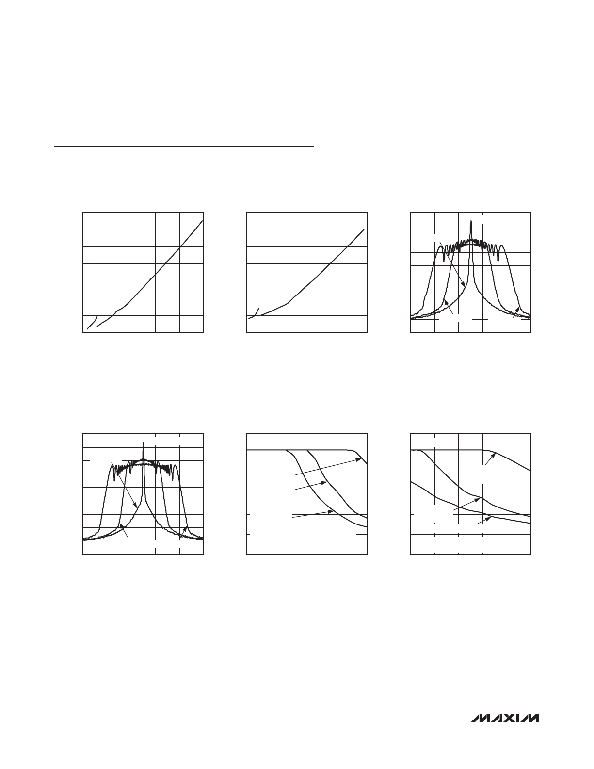
Typical Operating Characteristics
(V
AVDD
= V
DVDD
= V
= 3.3V, TA = +25NC, unless otherwise noted.)
IOVDD
TOTAL SUPPLY CURRENT
vs. TXCLKOUT_ FREQUENCY
(3-CHANNEL MODE)
210
MAX9268
PRBS PATTERN
200
ALL EQUALIZER MODES
ALL SPREAD MODES
190
180
170
160
TOTAL SUPPLY CURRENT (mA)
150
140
5 105
TXCLKOUT_ FREQUENCY (MHz)
OUTPUT POWER SPECTRUM
vs. TXCLKOUT_ FREQUENCY
(VARIOUS MAX9268 SPREAD)
-10
-20
0% SPREAD
-30
-40
-50
-60
-70
-80
OUTPUT POWER SPECTRUM (dBm)
-90
-100
61 71
2% SPREAD
TXCLKOUT_ FREQUENCY (MHz)
f
TXCLKOUT_
4% SPREAD
85654525
= 66MHz
69676563
TOTAL SUPPLY CURRENT
vs. TXCLKOUT_ FREQUENCY
(4-CHANNEL MODE)
210
PRBS PATTERN
200
MAX9268 toc01
ALL EQUALIZER MODES
ALL SPREAD MODES
190
180
170
160
TOTAL SUPPLY CURRENT (mA)
150
140
5 80
TXCLKOUT_ FREQUENCY (MHz)
MAXIMUM TXCLKOUT_ FREQUENCY
vs. STP CABLE LENGTH (BER < 10
120
100
MAX9268 toc04
OPTIMUM
80
PE/EQ SETTINGS
NO PE, 10.7dB
60
EQUALIZATION
40
NO PE, 5.2dB
EQUALIZATION
20
BER CAN BE AS LOW AS 10
MAXIMUM TXCLKOUT_ FREQUENCY (MHz)
CABLE LENGTHS LESS THAN 10m
0
0 20
STP CABLE LENGTH (m)
OUTPUT POWER SPECTRUM
vs. TXCLKOUT_ FREQUENCY
(VARIOUS MAX9268 SPREAD)
-10
-20
MAX9268 toc02
OUTPUT POWER SPECTRUM (dBm)
65503520
0% SPREAD
-30
-40
-50
-60
-70
-80
-90
-100
30.5 35.5
2% SPREAD
TXCLKOUT_ FREQUENCY (MHz)
f
TXCLKOUT_
4% SPREAD
= 33MHz
MAX9268 toc03
34.533.532.531.5
MAXIMUM TXCLKOUT_ FREQUENCY
vs. ADDITIONAL DIFFERENTIAL
-9
)
-12
FOR
15105
120
10m STP CABLE
100
MAX9268 toc05
80
60
NO PE, 10.7dB
40
EQUALIZATION
NO PE, 5.2dB EQUALIZATION
20
BER CAN BE AS LOW AS 10
MAXIMUM TXCLKOUT_ FREQUENCY (MHz)
FOR OPTIMUM PE/EQ SETTINGS
0
ADDITIONAL DIFFERENTIAL LOAD CAPACITANCE (pF)
C
(BER < 10-9)
L
PE/EQ SETTINGS
OPTIMUM
-12
MAX9268 toc06
FOR CL < 4pF
86420 10
6 ______________________________________________________________________________________
Page 7
Gigabit Multimedia Serial Link Deserializer
with LVDS System Interface
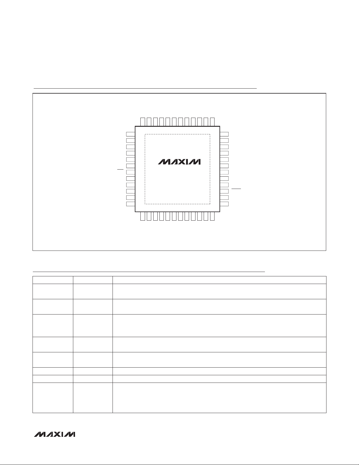
Pin Configuration
TXOUT1+
AVDD
AGND
TXOUT2-
TXOUT2+
TXCLKOUT-
TXCLKOUT+
TXOUT3-
TOP VIEW
TXOUT0-
TXOUT0+
36 35 34
TXOUT1-
33 32 31 30 29 28 27 26 25
TXOUT3+
MAX9268
AGND
GND
IOVDD
ADD0
ADD1
LOCK
ERR
MS
SSEN
DRS
AVDD
AGND
37
38
39
40
41
42
43
44
45
46
47
48
+
1
2
INT
BWS
MAX9268
EP
4
5
6
7
8
9
10
11
EQS
GPIO1
12
DVDD
GND
3
IN-
GPIO0
AVDD
IN+
AGND
CDS
24
23
22
21
20
19
18
17
16
15
14
13
AGND
AVDD
GND
IOVDD
CNTL2/MCLK
CNTL1
SD/CNTL0
SCK
WS
PWDN
TX/SCL
RX/SDA
TQFP
Pin Description
PIN NAME FUNCTION
1
BWS
2 INT
3 CDS
4 GPIO0
5, 23, 32, 47 AVDD
6, 7 IN+, IN- Differential CML Input. Differential input of the serial link.
8, 24, 31, 37, 48 AGND Analog Ground
9 EQS
Bus-Width Select. Output width selection requires external pulldown or pullup resistor. Set
BWS = low for 3-channel mode. Set BWS = high for 4-channel mode.
Interrupt Input. Requires external pulldown or pullup resistor. A transition on the MAX9268’s
INT input toggles the GMSL serializer’s INT output.
Control Direction Selection. Control link direction selection input requires external pulldown or
pullup resistor. Set CDS = low for FC on the GMSL serializer side of the serial link. Set CDS =
high for FC on the MAX9268 side of the serial link.
General-Purpose I/O 0. Open-drain, general-purpose input/output with internal 60kI (typ)
pullup resistor to IOVDD. GPIO0 is high impedance during power-up and when PWDN = low.
3.3V Analog Power Supply. Bypass AVDD to AGND with 0.1FF and 0.001FF capacitors as
close as possible to the device with the smaller capacitor closest to AVDD.
Equalizer Select Input. EQS requires external pulldown or pullup resistor. The state of EQS
latches upon power-up or when resuming from power-down mode (PWDN = low). Set
EQS = low for 10.7dB equalizer boost (EQTUNE = 1001). Set EQS = high for 5.2dB
equalizer boost (EQTUNE = 0100).
_______________________________________________________________________________________ 7
Page 8
Gigabit Multimedia Serial Link Deserializer
with LVDS System Interface
Pin Description (continued)
PIN NAME FUNCTION
10 GPIO1
11 DVDD
MAX9268
12, 22, 38 GND Digital and I/O Ground
13 RX/SDA
14 TX/SCL
15 PWDN Power-Down. Active-low power-down input requires external pulldown or pullup resistor.
16 WS I2S Word-Select Output
17 SCK I2S Serial-Clock Output
18 SD/CNTL0 I2S Serial-Data/Control Output. Disable I2S to use SD/CNTL0 as an additional control output.
19 CNTL1
20 CNTL2/MCLK
General-Purpose I/O 1. Open-drain general-purpose input/output with internal 60kI (typ)
pullup resistor to IOVDD. GPIO1 is high impedance during power-up and when PWDN = low.
3.3V Digital Power Supply. Bypass DVDD to GND with 0.1FF and 0.001FF capacitors as close
as possible to the device with the smaller capacitor closest to DVDD.
Receive/Serial Data. UART receive or I2C serial-data input/output with internal 30kI (typ)
pullup to IOVDD. In UART mode, RX/SDA is the Rx input of the MAX9268’s UART. In I2C
mode, RX/SDA is the SDA input/output of the MAX9268’s I2C master.
Transmit/Serial Clock. UART transmit or I2C serial-clock output with internal 30kI (typ) pullup
to IOVDD. In UART mode, TX/SCL is the Tx output of the MAX9268’s UART. In I2C mode, TX/
SCL is the SCL output of the MAX9268’s I2C master.
Control Output 1. CNTL1 is not active in 3-channel mode and remains low. To use CNTL1,
drive BWS high (4-channel mode) and set DISCNTL = 0. CNTL1 is mapped from DOUT27.
Control 2/MCLK Output. CNTL2/MCLK is not active in 3-channel mode and remains low.
To use CNTL2/MCLK, drive BWS high (4-channel mode). CNTL2/MCLK is mapped from
DOUT28. CNTL/MCLK can also be used to output MCLK (see the Additional MCLK Output for
Audio Applications section).
I/O Supply Voltage. 1.8V to 3.3V logic I/O power supply. Bypass IOVDD to GND with
21, 39 IOVDD
25, 26, 29, 30,
33–36
27, 28
40 ADD0
41 ADD1
42 LOCK
43 ERR
8 ______________________________________________________________________________________
TXOUT_+,
TXOUT_-
TXCLKOUT+,
TXCLKOUT-
0.1FF and 0.001FF capacitors as close as possible to the device with the smaller
capacitor closest to IOVDD.
Differential LVDS Data Outputs. Set BWS = low (3-channel mode) to use TXOUT0_ to
TXOUT2_. Set BWS = high (4-channel mode) to use TXOUT0_ to TXOUT3_.
Differential LVDS Output for the LVDS Clock
Address Selection Input 0. Three-level input to select the MAX9268’s device address
(see Table 2). The state of ADD0 latches upon power-up or when resuming from power-down
mode (PWDN = low).
Address Selection Input 1. Three-level input to select the MAX9268’s device address
(see Table 2). The state of ADD1 latches upon power-up or when resuming from power-down
mode (PWDN = low).
Open-Drain Lock Output with Internal 60kI (typ) Pullup to IOVDD. LOCK = high indicates
PLLs are locked with correct serial-word-boundary alignment. LOCK = low indicates PLLs are
not locked or incorrect serial-word-boundary alignment. LOCK remains low when the
configuration link is active. LOCK is high impedance when PWDN = low.
Active-Low, Open-Drain Video Data Error Output with Internal 60kI (typ) Pullup to IOVDD.
ERR goes low when the number of decoding errors during normal operation exceeds a programmed error threshold, or when at least one PRBS error is detected during PRBS test. ERR
is high impendence when PWDN = low.
Page 9
Gigabit Multimedia Serial Link Deserializer
with LVDS System Interface
Pin Description (continued)
PIN NAME FUNCTION
44 MS
45 SSEN
46 DRS
— EP
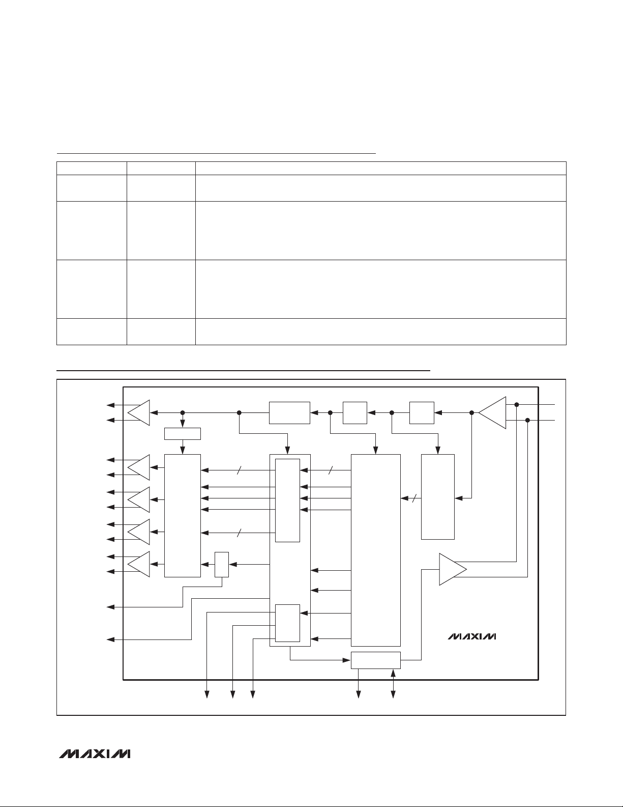
Functional Diagram
Mode Select. Control link mode-selection input requires an external pulldown or pullup resistor. Set MS = low to select base mode. Set MS = high to select bypass mode.
Spread-Spectrum Enable. Serial link spread-spectrum enable input requires an external pulldown or pullup resistor. The state of SSEN latches upon power-up or when resuming from
power-down mode (PWDN = low). Set SSEN = high for Q2% spread spectrum on the LVDS
and control outputs. Set SSEN = low to use the LVDS and control outputs without spread
spectrum.
Data-Rate Select. Data-rate range-selection input requires an external pulldown or pullup resistor.
The state of DRS latches upon power-up or when resuming from power-down mode (PWDN =
low). Set DRS = high for TXCLKOUT_ frequencies of 8.33MHz to 16.66MHz (3-channel mode), or
6.25MHz to 12.5MHz (4-channel mode). Set DRS = low for TXCLKOUT_ frequencies of 16.66MHz
to 104MHz (3-channel mode), or 12.5MHz to 78MHz (4-channel mode).
Exposed Pad. EP internally connected to AGND. MUST externally connect EP to the plane
supplying AGND for proper thermal and electrical performance.
MAX9268
TXCLKOUT+/-
TXOUT0+/-
TXOUT1+/-
TXOUT2+/-
TXOUT3+/-
CNTL1
(4-CH)
CNTL2/MCLK
(4-CH)
7x PLL
PARALLEL
TO LVDS
SSPLL
RGB[17:0]
HS HS
VS
DE
RGB[23:18] (4-CH)
RES/CNTL1
(4-CH)
VIDEO
FIFO
AUDIO
RGB
VS
DE
CNTL1/RES
CNTL2
ACB
FCC
CLK
DIV
8b/10b
DECODE/
UNSCRAMBLE
UART/I
CDR
PLL
SERIAL
TO
PARALLEL
REVERSE CONTROL
Rx/EQ
Tx
CHANNEL
IN+
IN-
MAX9268
2
C
SD/CNTL0 TX/SCL RX/SDASCK WS
_______________________________________________________________________________________ 9
Page 10
Gigabit Multimedia Serial Link Deserializer
with LVDS System Interface
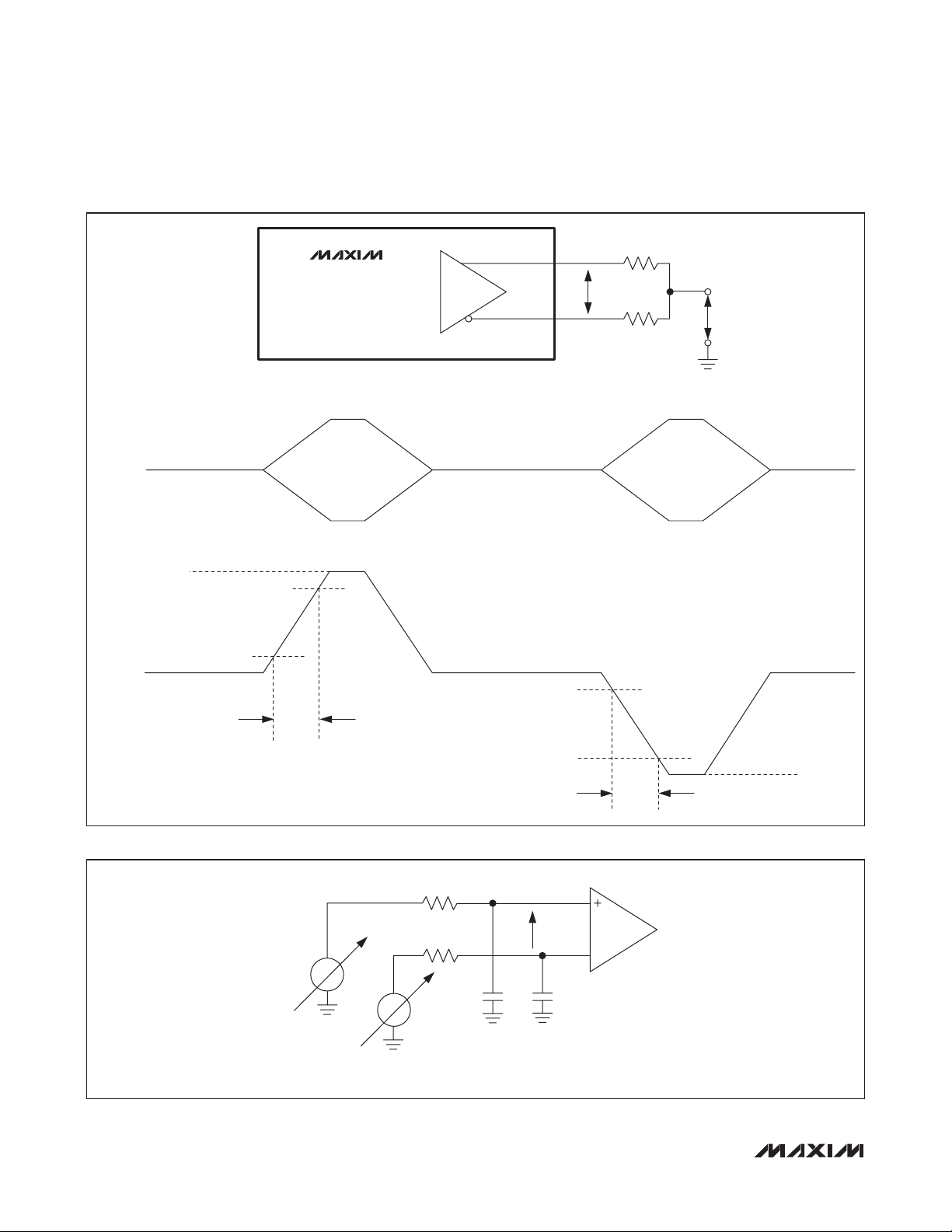
R
/2
IN+
L
MAX9268
V
OD
REVERSE
CONTROL-CHANNEL
TRANSMITTER
IN-
RL/2
V
CMR
MAX9268
IN+
V
CMR
IN-
V
ROH
0.9 x V
ROH
0.1 x V
(IN+) - (IN-)
ROH
t
R
Figure 1. Reverse Control-Channel Output Parameters
IN-
IN+
0.1 x V
ROL
0.9 x V
ROL
t
F
R
/2
L
IN+
V
ROL
V
RL/2
V
IN+
+
_
+
V
IN-
_
ID(P)
IN-
_
C
C
V
V
ID(P) =
CMR =
| V
(V
IN
- V
|
IN+
IN-
+ V
)/2
IN+
IN-
IN
Figure 2. Test Circuit for Differential Input Measurement
10 _____________________________________________________________________________________
Page 11
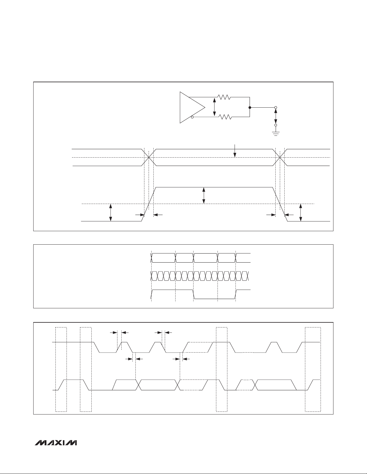
Gigabit Multimedia Serial Link Deserializer
TXOUT_-
TXCLKOUT-
TXOUT_+
TXCLKOUT+
(TXOUT_+) - (TXOUT_-)
(TXCLKOUT+) - (TXCLKOUT-)
with LVDS System Interface
MAX9268
TXOUT_+
TXCLKOUT+
TXOUT_-,
TXCLKOUT-
V
OS(-)
DV
OS
V
OD(-)
t
R
DVOD = |V
/2
R
L
V
OD
/2
R
L
((TXOUT_+) + (TXOUT_-))/2
((TXCLKOUT+) + (TXCLKOUT-))/2
V
OS(+)
= |V
- V
- V
OS(-)
OD(-)
|
|
OS(+)
VOD(+)
OD(+)
GND
V
OS
V
OS(-)
V
= 0V
OD
V
t
F
OD(-)
Figure 3. LVDS Output Parameters
Figure 4. Worst-Case Pattern Output
TX/
SCL
RX/
SDA
P
TXCLKOUT+
TXCLKOUT-
TXOUT0+ TO TXOUT3+
TXOUT0- TO TXOUT3-
CNTL_
t
R
t
HOLD
t
F
t
SET
PSS
Figure 5. I2C Timing Parameters
______________________________________________________________________________________ 11
Page 12

Gigabit Multimedia Serial Link Deserializer
with LVDS System Interface
(TXCLKOUT+) -
C
L
MAX9268
SINGLE-ENDED OUTPUT LOAD
0.8 x V
I0VDD
MAX9268
0.2 x V
I0VDD
t
R
Figure 6. Single-Ended Output Rise-and-Fall Times Figure 7. LVDS Output Pulse Position Measurement
t
F
(TXCLKOUT-)
(TXOUT_+) -
(TXOUT_-)
t
PPOS0
t
PPOS1
t
PPOS2
t
PPOS3
t
PPOS4
t
PPOS5
t
PPOS6
FIRST BIT
N
IN+/IN-
TXOUT_+/
TXOUT_-
TXCLKOUT+/-
N+1
Figure 8. Deserializer Delay
IN+/-
PWDN
LOCK
N+2...
V
EXPANDED TIME SCALE
FIRST BIT
N-1
t
SD
N
IN+ - IN-
LOCK
t
LOCK
PWDN MUST BE HIGH
V
OH
Figure 9. Lock Time
WS
t
t
DVA
IH1
t
PU
V
OH
SCK
SD
DVB
t
DVBtDVA
t
R
t
F
Figure 10. Power-Up Delay
Figure 11. Output I2S Timing Parameters
12 _____________________________________________________________________________________
Page 13

Gigabit Multimedia Serial Link Deserializer
with LVDS System Interface
Detailed Description
The MAX9268 deserializer with LVDS system interface utilizes Maxim’s GMSL technology. The MAX9268
deserializer pairs with any GMSL serializer to form a
complete digital serial link for joint transmission of highspeed video, audio, and bidirectional control data.
The MAX9268 allows a maximum serial payload data
rate of 2.5Gbps for greater than 15m of STP cable. The
deserializer operates up to 104MHz for 3-channel LVDS
or 78MHz for 4-channel LVDS. The operating frequency
range supports display panels from QVGA (320 x 240)
up to WXGA (1280 x 800) and higher with 24-bit color.
The 3-channel mode outputs an LVDS clock, three
lanes of LVDS data (21 bits), UART control signals,
and one I2S audio channel (consisting of three signals). The 4-channel mode outputs an LVDS clock, four
lanes of LVDS data (28 bits), UART control signals,
one I2S audio channel, and control signals. The I2S
interface supports sample rates from 8kHz to 192kHz
and audio word lengths of 4 to 32 bits. The embedded control channel forms a full-duplex, differential,
100kbps to 1Mbps UART link between the serializer and
deserializer. An ECU or FC can be located on the
serializer side of the link (typical for video display), on the
MAX9268
MAX9268 side of the link (typical for image sensing), or
on both sides. In addition, the control channel enables
ECU/FC control of peripherals in the remote side, such
as backlight control, grayscale Gamma correction,
camera module, and touch screen. Base-mode communication with peripherals uses either I2C or the GMSL
UART format. A bypass mode enables full-duplex communication using custom UART formats.
The MAX9268 channel equalizer, along with the
serializer preemphasis, extends the link length and
enhances the link reliability. Spread spectrum is available to reduce EMI on the LVDS and control outputs of
the MAX9268. The serial input complies with ISO 10605
and IEC 61000-4-2 ESD protection standards.
Register Mapping
The FC configures various operating conditions of the
GMSL serializer and the MAX9268 through internal
registers. The default device addresses are stored in registers 0x00 and 0x01 of both the GMSL serializer and the
MAX9268 (Table 1). Write to the 0x00 and 0x01 registers
in both devices to change the device address of the GMSL
serializer or the MAX9268.
Table 1. Power-Up Default Register Map (see Table 12)
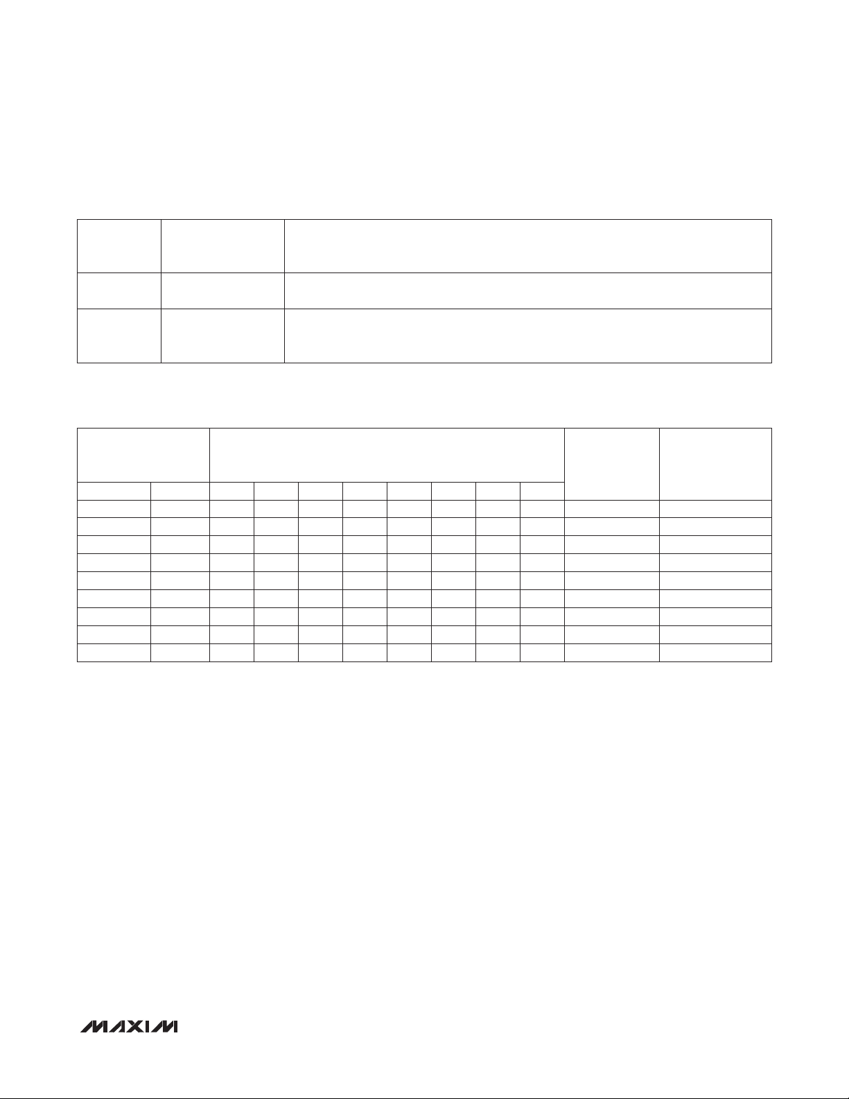
REGISTER
ADDRESS
(hex)
0x00
0x01
0x02 0x1F or 0x5F
0x03 0x00
POWER-UP
DEFAULT
(hex)
0x40, 0x44, 0x48
0x80, 0x84, 0x88,
0xC0, 0xC4, 0xC8
0x50, 0x54, 0x58,
0x90, 0x94, 0x98,
0xD0, 0xD4, 0xD8
POWER-UP DEFAULT SETTINGS
(MSB FIRST)
SERID = XX00XX0, serializer device address is determined by ADD1 and ADD0
(Table 2)
RESERVED = 0
DESID =XX01XX0, deserializer device address is determined by ADD1 and ADD0
(Table 2)
RESERVED = 0
SS = 00 (SSEN = low), SS = 01 (SSEN = high), spread-spectrum settings depend on
SSEN pin state at power-up
RESERVED = 0
AUDIOEN = 1, I2S channel enabled
PRNG = 11, automatically detect the pixel clock range
SRNG = 11, automatically detect serial-data rate
AUTOFM = 00, calibrate spread-modulation rate only once after locking
RESERVED = 0
SDIV = 00000, autocalibrate sawtooth divider
______________________________________________________________________________________ 13
Page 14

Gigabit Multimedia Serial Link Deserializer
with LVDS System Interface
Table 1. Power-Up Default Register Map (see Table 12) (continued)
REGISTER
ADDRESS
(hex)
MAX9268
0x04 0x03 or 0x13
0x05 0x24 or 0x29
0x06 0x0F
0x07 0x54 RESERVED = 01010100
0x08 0x30 RESERVED = 00110000
0x09 0xC8 RESERVED = 11001000
0x0A 0x12 RESERVED = 00010010
0x0B 0x20 RESERVED = 00100000
0x0C 0x00 ERRTHR = 00000000, error threshold set to zero for decoding errors
0x0D
0x0E
0x12 0x00
0x13 0xX0
POWER-UP
DEFAULT
(hex)
0x00
(read only)
0x00
(read only)
POWER-UP DEFAULT SETTINGS
(MSB FIRST)
LOCKED = 0, LOCK output is low (read only)
OUTENB = 0, outputs enabled
PRBSEN = 0, PRBS test disabled
SLEEP = 0 or 1, SLEEP setting default depends on CDS and MS pin state at power-up
(see the Link Startup Procedure section)
INTTYPE = 00, base mode uses I2C
REVCCEN = 1, reverse control channel active (sending)
FWDCCEN = 1, forward control channel active (receiving)
I2CMETHOD = 0, I2C master sends the register address
HPFTUNE = 01, 3.75MHz equalizer highpass cutoff frequency
PDHF = 0, high-frequency boosting disabled
EQTUNE = 0100 (EQS = high, 5.2dB), EQTUNE = 1001 (EQS = low, 10.7dB), EQTUNE
default setting depends on EQS pin state at power-up
RESERVED = 0
AUTORST = 0, error registers/output autoreset disabled
DISINT = 0, INT transmission enabled
INT = 0, INT output is low (read only)
GPIO1OUT = 1, GPIO1 output set to high
GPIO1 = 1, GPIO1 input = high (read only)
GPIO0OUT = 1, GPIO0 output set to high
GPIO0 = 1, GPIO0 input = high (read only)
DECERR = 00000000, zero decoding errors detected
PRBSERR = 00000000, zero PRBS errors detected
MCLKSRC = 0, MCLK is derived from PCLK (see Table 5)
MCLKDIV = 0000000, MCLK output is disabled
RESERVED = XXX
RESERVED = 10000
RESERVED = 00
FORCELVDS = 0, normal LVDS operation
0x14 0x01
14 _____________________________________________________________________________________
DCS = 0, normal CMOS driver current strength
DISCNTL1 = 0, serial-data bit 27 is mapped to CNTL1
DISRES = 0, serial-data bit 27 is mapped to RES
ILVDS = 01, 3.5mA LVDS output current
Page 15
Gigabit Multimedia Serial Link Deserializer
with LVDS System Interface
Table 1. Power-Up Default Register Map (see Table 12) (continued)
MAX9268
REGISTER
ADDRESS
(hex)
0x1E
0x1F
X = Don’t care.
POWER-UP
DEFAULT
(hex)
0x04
(read only)
0x0X
(read only)
POWER-UP DEFAULT SETTINGS
(MSB FIRST)
ID = 00000100, device ID is 0x04
RESERVED = 000
CAPS = 0, not HDCP capable
REVISION = XXXX
Table 2. Deserializer Device Address Defaults (Register 0x01)
PIN
ADD1 ADD0 D7 D6 D5 D4 D3 D2 D1 D0
Low Low 1 0 0 X** 0 0 0
Low High 1 0 0 X** 0 1 0
Low Open 1 0 0 X** 1 0 0
High Low 1 1 0 X** 0 0 0
High High 1 1 0 X** 0 1 0
High Open 1 1 0 X** 1 0 0
Open Low 0 1 0 X** 0 0 0
Open High 0 1 0 X** 0 1 0
Open Open 0 1 0 X** 1 0 0
*ADD0 and ADD1 affect the default device address values stored in the MAX9268 only. The default device address values stored
in the GMSL serializer may differ (see the 3-Level Inputs for Default Device Address section).
**X = 0 for the serializer address, X = 1 for the deserializer address.
DEVICE ADDRESS*
(bin)
R/W
R/W
R/W
R/W
R/W
R/W
R/W
R/W
R/W
SERIALIZER
DEVICE
ADDRESS*
(hex)
80 90
84 94
88 98
C0 D0
C4 D4
C8 D8
40 50
44 54
48 58
DESERIALIZER
DEVICE
ADDRESS*
(hex)
______________________________________________________________________________________ 15
Page 16

Gigabit Multimedia Serial Link Deserializer
with LVDS System Interface
Typical Bitmapping and
Bus-Width Selection
The LVDS output has two selectable widths: 3-channel
and 4-channel. The MAX9268 outputs 3- or 4-channel
LVDS (Table 3). Serial data is mapped to outputs on the
MAX9268 according to Figures 12 and 13. In 3-channel mode, TXOUT3_ and CNTL1, CNTL2/MCLK are not
available. For both modes, the SD/CNTL0, SCK, and WS
MAX9268
pins are for I2S audio when audio is enabled. With audio
disabled, SD/CNTL0 becomes control signal CNTL0.
The MAX9268 outputs clock rates from 8.33MHz to
104MHz for 3-channel mode and 6.25MHz to 78MHz for
4-channel mode.
Serial Link Signaling and Data Format
The GMSL high-speed serial link uses CML signaling
with programmable preemphasis and AC-coupling. The
GMSL deserializer uses AC-coupling and programmable
channel equalization. When using both the preemphasis
and equalization, including internally generated over-
head bits, the GMSL link operates up to 3.125Gbps over
STP cable lengths of 15m or greater. The payload data
rate, which is the data rate available to the user or the
data rate after subtracting overhead, is 2.5Gbps.
The GMSL serializer scrambles and encodes the input
data and sends the 8b/10b coded signal through the
serial link. The MAX9268 deserializer recovers the
embedded serial clock and then samples, decodes, and
descrambles before outputting the data. Figures 14 and
15 show the serial-data packet format after unscrambling
and 8b/10b decoding. In 3-channel or 4-channel mode,
21 or 28 bits map to the TXOUT_ _ LVDS outputs. Serialdata bits 27 and 28 map to control outputs in 4-channel
mode. The audio channel bit (ACB) contains an encoded
audio signal derived from the three I2S signals (SD/
CNTL0, SCK, and WS). The forward control-channel
(FCC) bit carries the forward control data. The last bit
(PCB) is the parity bit of the previous 23 or 31 bits.
Table 3. Bus-Width Selection Using BWS
3-CHANNEL MODE
OUTPUT BITS
TYPICAL BITMAPPING
DOUT[0:5] R[0:5] — R[0:5] —
DOUT[6:11] G[0:5] — G[0:5] —
DOUT[12:17] B[0:5] — B[0:5] —
DOUT[18:20] HS, VS, DE — HS, VS, DE —
DOUT[21:22] Not used Not used R6, R7 —
DOUT[23:24] Not used Not used G6, G7 —
DOUT[25:26] Not used Not used B6, B7 —
DOUT27 Not used Not used RES* CNTL1*
DOUT28 Not used Not used — CNTL2/MCLK
SD — SD/CNTL0 — SD/CNTL0
*See the Reserved Bit (RES)/CNTL1 section for details.
(BWS = LOW)
AUXILIARY SIGNALS
MAPPING
TYPICAL BITMAPPING
4-CHANNEL MODE
(BWS = HIGH)
AUXILIARY SIGNALS
MAPPING
16 _____________________________________________________________________________________
Page 17

Gigabit Multimedia Serial Link Deserializer
with LVDS System Interface
TXCLKOUT-
TXCLKOUT+
TXOUT0+/TXOUT0-
CYCLE N-1
DOUT0 DOUT6 DOUT5 DOUT4 DOUT3 DOUT2 DOUT1 DOUT0
DOUT1
CYCLE N
MAX9268
TXOUT1+/TXOUT1-
TXOUT2+/TXOUT2-
TXOUT3+/TXOUT3-
CNTL2/MCLK
SD/CNTL0
Figure 12. LVDS Output Timing
TXCLKOUT-
TXCLKOUT+
CNTL1
DOUT8 DOUT7 DOUT13 DOUT12 DOUT11 DOUT10 DOUT9 DOUT8 DOUT7
DOUT15 DOUT14 DOUT20 DOUT19 DOUT18 DOUT17 DOUT16 DOUT15 DOUT14
DOUT22 DOUT21
*ONLY WHEN I
2
S IS DISABLED.
DOUT27 DOUT26 DOUT25 DOUT24 DOUT23 DOUT22 DOUT21
DOUT27
DOUT28
SD*
CYCLE N-1 CYCLE N
TXOUT0+/TXOUT0-
TXOUT1+/TXOUT1-
TXOUT2+/TXOUT2-
TXOUT3+/TXOUT3-
R1
G2 G1 B1 B0 G5 G4 G3 G2 G1
B3 B2 DE VS HS B5 B4 B3 B2
R7 R6 RES B7 B6 G7 G6 R7 R6
Figure 13. Typical Panel Clock and Bit Assignment
______________________________________________________________________________________ 17
R0 G0 R5 R4 R3 R2 R1 R0
Page 18

Gigabit Multimedia Serial Link Deserializer
with LVDS System Interface
24 BITS
DOUT0
DOUT1 DOUT17 DOUT18 DOUT19 DOUT20 ACB FCC PCB
R0 R1 B5 HS VS DE
MAX9268
NOTE: TYPICAL LOCATIONS OF THE RGB DATA AND CONTROL SIGNALS.
Figure 14. 3-Channel Mode Serial Link Data Format
DOUT1
DOUT0
R0 HS
R1
(TXOUT[2:0]_)
NOTE: TYPICAL LOCATIONS OF THE LVDS RGB DATA AND CONTROL SIGNALS.
*DOUT27 OUTPUTS TO LVDS DATA (TXOUT3_) AND/OR EXTERNAL PIN (CNTL1).
Figure 15. 4-Channel Mode Serial Link Data Format
DOUT18 DOUT19 DOUT20
DOUT17
B5 VS DE
LVDS
DATA
LVDS
DATA
(3 CHANNELS)
32 BITS
DOUT21
DOUT22 DOUT25 DOUT26 DOUT27 DOUT28 ACB FCC PCB
DOUT23
R6 R7 B6
AUDIO
CHANNEL BIT
FORWARD
CONTROL-
CHANNEL BIT
PACKET
PARITY
CHECK BIT
DOUT24
G7
G6 B7 CNTL2
LVDS
DATA
(TXOUT3_)
RES/CNTL1*
CHANNEL/CNTL0
AUDIO
BIT
FORWARD
CONTROL-
CHANNEL BIT
PACKET
PARITY
CHECK BIT
Reserved Bit (RES)/CNTL1
In 4-channel mode, the MAX9268 deserializes serialdata bit 27 to both RES and CNTL1 by default (both
DISCNTL and DISRES = 0). Setting DISRES (D2 of
register 0x14) = 1 forces RES low. Setting DISCNTL1 (D3
of register 0x14) = 1 forces CNTL1 low.
Reverse Control Channel
The GMSL serializer uses the reverse control
channel to receive I2C/UART and interrupt signals from
the MAX9268 in the opposite direction of the video
channel for 350Fs after starting/stopping the forward
serial link.
Data-Rate Selection
The MAX9268 uses the DRS input to set the TXCLKOUT_
frequency. Set DRS high for a TXCLKOUT_ frequency
of 6.25MHz to 12.5MHz (4-channel mode), or 8.33MHz
to 16.66MHz (3-channel mode). Set DRS low for normal
operation with a TXCLKOUT_ frequency of 12.5MHz
to 78MHz (4-channel mode), or 16.66MHz to 104MHz
(3-channel mode).
stream. The reverse control channel and forward video
data coexist on the same twisted pair forming a bidirectional link. The reverse control channel operates independently from the forward control channel. The reverse
control channel is available 500Fs after power-up. The
GMSL serializer temporarily disables the reverse control
18 _____________________________________________________________________________________
The I2S audio channel supports audio sampling rates
from 8kHz to 192kHz and audio word lengths from 4 bits
to 32 bits. The audio bit clock (SCK) does not have to
be synchronized with TXCLKOUT_. The GMSL serializer
automatically encodes audio data into a single bit stream
Audio Channel
Page 19

Gigabit Multimedia Serial Link Deserializer
with LVDS System Interface
synchronous with TXCLKOUT_. The MAX9268 deserializer decodes the audio stream and stores audio words
in a FIFO. Audio rate detection uses an internal oscillator
to continuously determine the audio data rate and output
the audio in I2S format. The audio channel is enabled by
default. When the audio channel is disabled, the audio
data input (SD) on the serializer becomes a control input
(CNTL0) and SD/CNTL0 becomes a control output on
the deserializer.
Low TXCLKOUT_ frequencies limit the maximum
audio sampling rate. Table 4 lists the maximum audio
sampling rate for various TXCLKOUT_ frequencies.
Spread-spectrum settings do not affect the I2S data rate
or WS clock frequency.
Additional MCLK Output for
Audio Applications
Some audio DACs such as the MAX9850 do not require
a synchronous main clock (MCLK), while other DACs
require MCLK to be a specific multiple of WS. If the audio
DAC chip needs the MCLK to be a multiple of WS, use
an external PLL to regenerate the required MCLK from
WS or SCK.
For audio applications that have WS synchronous to
TXCLKOUT_, the MAX9268 provides a divided clock
output on CNTL2/MCLK at the expense of one less
control line in 4-channel mode (3-channel mode is not
affected). By default, CNTL2/MCLK operates as a con-
trol data output, and MCLK is turned off. Set MCLKDIV
(MAX9268 register 0x12, D[6:0]) to a nonzero value
to enable the MCLK output. Set MCLKDIV to 0x00 to
disable MCLK and set CNTL2/MCLK as a control data
output.
The output MCLK frequency is:
f
SRC
=
MCLKDIV
where:
f
f
MCLK
= the MCLK source frequency (Table 5)
SRC
MCLKDIV = the divider ratio from 1 to 127
Choose MCLKDIV values such that f
MCLK
is not
greater than 60MHz. MCLK frequencies derived from
TXCLKOUT_ (MSCLKSRC = 0) are not affected by
spread-spectrum settings in the MAX9268. However,
enabling spread spectrum in the GMSL serializer introduces spread spectrum into MCLK. Spread-spectrum
settings of either device do not affect MCLK frequencies
derived from the internal oscillator. The internal oscillator frequency ranges from 100MHz to 150MHz over all
process corners and operating conditions.
MAX9268
Table 4. Maximum Audio WS Frequency (kHz) for Various TXCLKOUT_ Frequencies
WORD
LENGTH
(BITS)
8 > 192 > 192 > 192 > 192 > 192 > 192 > 192 > 192
16 > 192 > 192 > 192 > 192 > 192 > 192 > 192 > 192
18 185.5 > 192 > 192 > 192 185.5 > 192 > 192 > 192
20 174.6 > 192 > 192 > 192 174.6 > 192 > 192 > 192
24 152.2 182.7 > 192 > 192 152.2 182.7 > 192 > 192
32 123.7 148.4 164.3 > 192 123.7 148.4 164.3 > 192
Table 5. f
MCLKSRC SETTING
(REGISTER 0x12, D7)
12.5 15 16.6 > 20 6.25 7.5 8.33 > 10
Settings
SRC
0
1 — —
TXCLKOUT_ FREQUENCY
(DRS = LOW)
(MHz)
DATA-RATE SETTING BUS-WIDTH SETTING MCLK SOURCE FREQUENCY (f
High speed
Low speed
3-channel mode 3 x f
4-channel mode 4 x f
3-channel mode 6 x f
4-channel mode 8 x f
TXCLKOUT_ FREQUENCY
(DRS = HIGH)
(MHz)
SRC
TXCLKOUT_
TXCLKOUT_
TXCLKOUT_
TXCLKOUT_
Internal oscillator
(120MHz, typ)
)
______________________________________________________________________________________ 19
Page 20

Gigabit Multimedia Serial Link Deserializer
with LVDS System Interface
Control Channel and Register Programming
The control channel is available for the FC to send and
receive control data over the serial link simultaneously with
the high-speed data, to program registers on the link serializer/deserializer or to program peripherals. Configuring the
CDS pin allows a FC to control the link from the side of the
serializer or deserializer, or with dual FCs from both sides,
to support a wide variety of applications.
MAX9268
The control channel runs in base mode or bypass mode
according to the mode-selection (MS) input of the device
connected to the FC. In base mode, the control-channel
transactions are half-duplex and in bypass mode they are
full-duplex.
Base Mode
In base mode the FC is the host, and in order to access the
registers of the serializer or deserializer it must use the
GMSL UART format and protocol. The FC accesses
peripherals with an I2C interface by sending GMSL UART
packets, which are converted to I2C by the serializer
or deserializer on the remote side of the link. The FC
communicates with a UART peripheral in base mode
(through INTTYPE register settings) using the GMSL UART
protocol. The device addresses of the GMSL serializer and
MAX9268 in base mode are programmable. The default
MAX9268 device address is determined by ADD0 and
ADD1 upon power-up, or after returning from a powerdown state (Table 2).
When the peripheral interface uses I2C (default), the GMSL
serializer/MAX9268 convert packets to I2C that have device
addresses different from those of the GMSL serializer or
MAX9268. The converted I2C bit rate is the same as the
original UART bit rate.
The GMSL serializer embeds control signals going to the
MAX9268 in the high-speed forward link. The MAX9268
uses a proprietary differential line coding to send signals
back towards the serializer. The speed of the control channel ranges from 100kbps to 1Mbps in both directions. The
GMSL serializer and MAX9268 deserializer automatically
detect the control-channel bit rate in base mode. Packet bit
rates can vary up to 3.5x from the previous bit rate (see the
Changing the Clock Frequency section). Figure 16 shows
the UART protocol for writing and reading in base mode
between the FC and the GMSL serializer/MAX9268.
Figure 17 shows the UART data format. Figures 18 and 19
detail the formats of the SYNC byte (0x79) and the ACK
byte (0xC3). The FC and the connected slave chip generate the SYNC byte and ACK byte, respectively. Events
such as device wake-up and interrupt generate transitions
on the control channel that should be ignored by the FC.
Data written to the GMSL serializer/MAX9268 registers do
not take effect until after the acknowledge byte is sent.
This allows the FC to verify write commands received without error, even if the result of the write command directly
affects the serial link. The slave uses the SYNC byte to
synchronize with the host UART data rate automatically. If
the INT or MS inputs of the MAX9268 toggle while there is
control-channel communication, the control-channel communication can be corrupted since INT has priority on the
control channel. In the event of a missed acknowledge, the
FC should assume there was an error in the packet when
the slave device receives it, or that an error occurred during
the response from the slave device. In base mode, the FC
must keep the UART Tx/Rx lines high for 16 bit times before
sending a new packet.
As shown in Figure 20, the remote-side device converts
the packets going to or coming from the peripherals from
the UART format to the I2C format and vice versa. The
remote device removes the byte number count and adds or
receives the ACK between the data bytes of I2C. The I2C’s
data rate is the same as the UART data rate.
WRITE DATA FORMAT
SYNC DEV ADDR + R/W REG ADDR NUMBER OF BYTES BYTE 1 BYTE N
MASTER WRITES TO SLAVE
MASTER READS FROM SLAVE
READ DATA FRMAT
SYNC DEV ADDR + R/W REG ADDR NUMBER OF BYTES
MASTER WRITES TO SLAVE
MASTER READS FROM SLAVE
Figure 16. GMSL UART Protocol for Base Mode
20 _____________________________________________________________________________________
ACK
BYTE NBYTE 1ACK
Page 21

Gigabit Multimedia Serial Link Deserializer
with LVDS System Interface
1 UART FRAME
START D0 D1 D2 D3 D4 D5 D6 D7 PARITY STOP
MAX9268
FRAME 1
STOP START STOP START
FRAME 2 FRAME 3
Figure 17. GMSL UART Data Format for Base Mode
D1 D2 D3 D4 D5 D6 D7
STARTD01 0 0 1 1 1 1 0
PARITY STOP
STARTD01 1 0 0 0 0 1 1
D1 D2 D3 D4 D5 D6 D7
Figure 18. SYNC Byte (0x79) Figure 19. ACK Byte (0xC3)
2
UART-TO-I
FC
GMSL SERIALIZER/MAX9268
C CONVERSION OF WRITE PACKET (I2CMETHOD = 0)
GMSL SERIALIZER/MAX9268
11
SYNC FRAME REGISTER ADDRESS NUMBER OF BYTESDEVICE ID + WR DATA 0
11 11 11 11
PERIPHERAL
1 11
7
DEV ID A
S
W1REG ADDR8A
1 1 8 1
8
DATA 0 A DATA N A P
11 11
DATA N
PARITY STOP
ACK FRAME
2
UART-TO-I
FC
GMSL SERIALIZER/MAX9268 PERIPHERAL
C CONVERSION OF READ PACKET (I2CMETHOD = 0)
GMSL SERIALIZER/MAX9268
11
SYNC FRAME REGISTER ADDRESS NUMBER OF BYTESDEVICE ID + RD
11 11 11 11
: MASTER TO SLAVE
1 17W1
DEV ID AS
REG ADDR8A
1
: SLAVE TO MASTER
ACK FRAME
1 17R1
DEV ID AS
S: START P: STOP A: ACKNOWLEDGE
1
DATA 08A
11
DATA 0
DATA N P18A
Figure 20. Format Conversion between GMSL UART and I2C with Register Address (I2CMETHOD = 0)
______________________________________________________________________________________ 21
11
DATA N
1
Page 22

Gigabit Multimedia Serial Link Deserializer
with LVDS System Interface
Interfacing Command-Byte-Only I2C Devices
The GMSL serializer and MAX9268 UART-to-I2C
conversion interfaces with devices that do not require
register addresses, such as the MAX7324 GPIO expander. In this mode, the I2C master ignores the register
address byte and directly reads/writes the subsequent
data bytes (Figure 21). Change the communication
method of the I2C master using the I2CMETHOD bit.
MAX9268
I2CMETHOD = 1 sets command-byte-only mode, while
I2CMETHOD = 0 sets normal mode where the first byte
in the data stream is the register address.
Bypass Mode
In bypass mode, the GMSL serializer/MAX9268 ignore
UART communications. The FC is thereby free to
communicate with the peripherals using its own UART
protocol without concern that communication traffic
inadvertently misprograms the GMSL serializer or
MAX9268. The FC cannot access the GMSL serializer/
MAX9268 registers in this mode. Peripherals accessed
through the forward control channel using the UART
interface need to handle at least one TXCLKOUT_ period
of jitter due to the asynchronous sampling of the UART
signal by TXCLKOUT_.
Set MS = high to put the control channel into bypass
mode. For applications with the FC connected to the
deserializer (CDS is high), there is a 1ms wait time
between setting MS high and the bypass control channel
being active. There is no delay time when switching to
bypass mode when the FC is connected to the serializer
(CDS = low). Bypass mode accepts bit rates down to
28kbps in the forward direction (serializer to deserializer), and 7.7kbps in the reverse direction (deserializer to
serializer). See the Interrupt Control section for interrupt
functionality limitations. The control-channel data pattern
should not be held low longer than 100µs if interrupt
control is used.
Interrupt Control
The INT pin of the GMSL serializer is the interrupt output
and the INT pin of the MAX9268 is the interrupt input.
The interrupt output on the GMSL serializer follows the
transitions at the interrupt input, even during reversechannel communication or loss of lock. This interrupt
function supports remote-side functions such as touchscreen peripherals, remote power-up, or remote monitoring. Interrupts that occur during periods where the
reverse control channel is disabled, such as link startup/
shutdown, are automatically resent once the reverse
control channel becomes available again. Bit D4 of
register 0x06 in the MAX9268 also stores the interrupt
input state. The INT output of the GMSL serializer is low
after power-up. In addition, the FC can set the INT output
of the serializer by writing to the SETINT register bit. In
normal operation, the state of the interrupt output
changes when the interrupt input on the MAX9268 toggles.
Do not send a logic-low value longer than 100Fs in
either base or bypass mode to ensure proper interrupt
functionality.
2
C CONVERSION OF WRITE PACKET (I2CMETHOD = 1)
UART-TO-I
GMSL SERIALIZER/MAX9268FC
11 11 11 11 11 11 11
SYNC FRAME DEVICE ID + WR REGISTER ADDRESS NUMBER OF BYTES DATA 0 DATA N ACK FRAME
GMSL SERIALIZER/MAX9268
2
UART-TO-I
FC
SYNC FRAME
GMSL SERIALIZER/MAX9268
Figure 21. Format Conversion Between GMSL UART and I2C with Register Address (I2CMETHOD = 1)
22 _____________________________________________________________________________________
C CONVERSION OF READ PACKET (I2CMETHOD = 1)
GMSL SERIALIZER/MAX9268
PERIPHERAL
1111 11 11 11 11 11
DEVICE ID + RD REGISTER ADDRESS NUMBER OF BYTES
PERIPHERAL
: MASTER TO SLAVE
: SLAVE TO MASTER S: START P: STOP A: ACKNOWLEDGE
1 1 1 8
DEV ID R A A A PDATA 0 DATA N
S
ACK FRAME DATA 0 DATA N
8 81111 7 1 1
1 1 17
DATA NADATA 0W ADEV IDS A P
8
Page 23

Gigabit Multimedia Serial Link Deserializer
with LVDS System Interface
Line Equalizer
The MAX9268 includes an adjustable line equalizer to
further compensate cable attenuation at high frequencies.
The cable equalizer has 12 selectable levels of compensation, from 2.1dB to 13dB (Table 6). The EQS input selects
the default equalization level at power-up. The state of EQS
is latched upon power-up or when resuming from powerdown mode. To select other equalization levels, set the
corresponding register bits in the MAX9268 (0x05 D[3:0]).
Use equalization in the MAX9268, together with preemphasis in the GMSL serializer, to create the most reliable link
for a given cable.
Spread Spectrum
To reduce the EMI generated by the transitions on the serial
link and outputs of the MAX9268, both the GMSL serializer and MAX9268 support spread spectrum. Turning on
spread spectrum on the GMSL serializer spreads the serial
data and the MAX9268 outputs. Do not enable spread for
both the GMSL serializer and the MAX9268. The two selectable spread-spectrum rates at the MAX9268 outputs are
Q2% and Q4% (Table 7).
Set the MAX9268 SSEN input high to select 2% spread
at power-up, and SSEN input low to select no spread at
power-up. The state of SSEN is latched upon power-up or
when resuming from power-down mode.
Turning on spread spectrum on the GMSL serializer or the
MAX9268 does not affect the audio data stream. Changes
in the GMSL serializer spread settings only affect the
MAX9268 MCLK output if it is derived from TXCLKOUT_
(MCLKSRC = 0).
The MAX9268 includes a sawtooth divider to control the
spread-modulation rate. Autodetection or manual programming of the TXCLKOUT_ operation range guarantees a
spread-spectrum modulation frequency within 20kHz to
40kHz. Additionally, manual configuration of the sawtooth
divider (SDIV, 0x03 D[4:0]) allows the user to set a modulation frequency according to the TXCLKOUT_ frequency.
Always keep the modulation frequency between 20kHz to
40kHz to ensure proper operation.
Manual Programming of the
Spread-Spectrum Divider
The modulation rate for the MAX9268 relates to the
TXCLKOUT_ frequency as follows:
f
f 1 DRS
= +
( )
where:
fM = Modulation frequency
DRS = DRS input value (0 or 1)
f
TXCLKOUT_
MOD = Modulation coefficient given in Table 8
SDIV = 5-bit SDIV setting, manually programmed by the FC
To program the SDIV setting, first look up the modulation
coefficient according to the spread-spectrum settings.
M
= LVDS clock frequency
TXCLKOUT_
MOD SDIV
×
MAX9268
Table 6. Cable Equalizer Boost Levels
BOOST SETTING
(0x05 D[3:0])
0000 2.1
0001 2.8
0010 3.4
0011 4.2
0100
0101 6.2
0110 7
0111 8.2
1000 9.4
1001
1010 11.7
1011 13
______________________________________________________________________________________ 23
TYPICAL BOOST GAIN (dB)
5.2
Power-up default
(EQS = high)
10.7
Power-up default
(EQS = low)
Table 7. LVDS and Control Output Spread
Rates
SS SPREAD (%)
00
01
10 No spread spectrum
11
No spread spectrum.
Power-up default when SSEN = low.
Q2% spread spectrum.
Power-up default when SSEN = high.
Q4% spread spectrum
Table 8. Modulation Coefficients and
Maximum SDIV Settings
SPREAD-
SPECTRUM
SETTING (%)
4 208 15
2 208 30
MODULATION
COEFFICIENT
(dec)
SDIV UPPER
LIMIT (dec)
Page 24

Gigabit Multimedia Serial Link Deserializer
with LVDS System Interface
Solve the above equation for SDIV using the desired pixel
clock and modulation frequencies. If the calculated SDIV
value is larger than the maximum allowed SDIV value in
Table 8, set SDIV to the maximum value.
Sleep Mode
The GMSL serializer/MAX9268 include low-power sleep
mode to reduce power consumption on the device not
attached to the FC (the MAX9268 in LCD applications and
MAX9268
the GMSL serializer in camera applications). Set the corresponding remote IC’s SLEEP bit to 1 to initiate sleep mode.
The GMSL serializer sleeps immediately after setting its
SLEEP = 1. The MAX9268 sleeps after serial link inactivity
or 8ms (whichever arrives first) after setting its SLEEP = 1.
See the Link Startup Procedure section for details on wak-
ing up the device for different FC and starting conditions.
The FC side device cannot enter into sleep mode. If an
attempt is made to program the FC side device for sleep,
the SLEEP bit remains 0. Use the power-down mode to
bring the FC side device into a low-power state.
Power-Down Mode
The MAX9268 includes a power-down mode to further
reduce power consumption. Set PWDN low to enter power-
down mode. While in power-down mode, the outputs of
the device remain high impedance. Entering power-down
mode resets the internal registers of the device. In addition,
upon exiting power-down mode, the MAX9268 relatches
the state of SSEN, EQS, DRS, and ADD_.
Configuration Link Mode
The GMSL includes a low-speed configuration link to allow
control-data connection between the two devices in the
absence of a valid clock input. In either display or camera
applications, the configuration link can be used to program
equalizer/preemphasis or other registers before establishing the video link. An internal oscillator provides a clock
for establishing the serial configuration link between the
GMSL serializer and the MAX9268. Set CLINKEN = 1 on
the GMSL serializer to turn on the configuration link. The
configuration link remains active as long as the video link
has not been enabled. The video link overrides the configuration link and attempts to lock when SEREN = 1.
Link Startup Procedure
Table 9 lists four startup cases for video-display applications. Table 10 lists two startup cases for image-sensing
applications. In either video-display or image-sensing
applications, the control link is always available after the
high-speed data link or the configuration link is established
and the GMSL serializer/MAX9268 registers or peripherals
are ready for programming.
Video-Display Applications
For a video-display application with a remote display unit,
connect the FC to the GMSL serializer and set CDS = low
for both the GMSL serializer and the MAX9268. Table 9
summarizes the four startup cases based on the settings
of AUTOS and MS.
Case 1: Autostart Mode
After power-up or when PWDN transitions from low to
high for both the serializer and deserializer, the serial link
establishes whether a stable clock is present. The GMSL
serializer locks to the clock and sends the serial data to the
MAX9268. The MAX9268 then detects activity on the serial
link and locks to the input serial data.
Case 2: Standby Start Mode
After power-up or when PWDN transitions from low to high
for both the serializer and deserializer, the MAX9268 starts
up in sleep mode, and the GMSL serializer stays in standby
mode (does not send serial data). Use the FC and program
the serializer to set SEREN = 1 to establish a video link
or CLINKEN = 1 to establish the configuration link. After
locking to a stable clock (for SEREN = 1) or the internal
oscillator (for CLINKEN = 1), the serializer sends a wakeup signal to the MAX9268. The MAX9268 exits sleep mode
after locking to the serial data and sets SLEEP = 0. If after
8ms the MAX9268 does not lock to the input serial data, the
deserializer goes back to sleep and the internal sleep bit
remains set (SLEEP = 1).
Case 3: Remote Side Autostart Mode
After power-up or when PWDN transitions from low to
high, the remote device (MAX9268) starts up and tries to
lock to an incoming serial signal with sufficient power. The
host side (GMSL serializer) is in standby mode and does
not try to establish a link. Use the FC and program the
serializer to set SEREN = 1 (and apply a stable clock signal)
to establish a video link, or CLINKEN = 1 to establish the
configuration link. In this case, the MAX9268 ignores the
short wake-up signal sent from the GMSL serializer.
Case 4: Remote Side in Sleep Mode
After power-up or when PWDN transitions from low to high,
the remote device (MAX9268) starts up in sleep mode.
The high-speed link establishes automatically after the
GMSL serializer powers up with a stable clock signal and
sends a wake-up signal to the MAX9268. Use this mode in
applications where the MAX9268 powers up before the
GMSL serializer.
24 _____________________________________________________________________________________
Page 25

Gigabit Multimedia Serial Link Deserializer
with LVDS System Interface
Table 9. Startup Selection for Display Applications (CDS = Low)
MAX9268
CASE
SERIALIZER)
1 Low
2 High
3 High
4 Low
AUTOS
(GMSL
GMSL SERIALIZER
POWER-UP STATEMS(MAX9268)
Serialization
enabled
Serialization
disabled
Serialization
disabled
Serialization
enabled
SLEEP = 1, VIDEO LINK OR CONFIG
LINK NOT LOCKED AFTER 8ms
Low
High
Low
High
MAX9268
POWER-UP STATE
Normal
(SLEEP = 0)
Sleep mode
(SLEEP = 1)
Normal
(SLEEP = 0)
In sleep mode
(SLEEP = 1)
LINK STARTUP MODE
Both devices power up with serial link
active (autostart).
Serial link is disabled and the
MAX9268 powers up in sleep mode.
Set SEREN = 1 or CLINKEN = 1 in the
GMSL serializer to start the serial link
and wake up the MAX9268.
Both devices power up in normal
mode with the serial link disabled. Set
SEREN = 1 or CLINKEN = 1 in the
GMSL serializer to start the serial link.
MAX9268 starts in sleep mode. Link
autostarts upon GMSL serializer
power-up. Use this case when the
MAX9268 powers up before the
serializer.
MS PIN
SETTING
LOW
HIGH
SEND INT TO
GMSL SERIALIZER
SLEEP BIT
POWER-UP VALUE
0
1
SERIAL LINK ACTIVITY STOPS OR 8ms ELAPSES AFTER
INT CHANGES FROM
LOW TO HIGH OR
HIGH TO LOW
SLEEP
FC SETS SLEEP = 1
ALL STATES
WAKE-UP
SIGNAL
PWDN = LOW OR
POWER-OFF
Figure 22. State Diagram, CDS = Low (LCD Application)
______________________________________________________________________________________ 25
POWER-ON
IDLE
POWER-DOWN
OR
POWER-OFF
SIGNAL
DETECTED
PWDN = HIGH,
POWER-ON
SERIAL PORT
VIDEO LINK
LOCKED
VIDEO LINK
OPERATING
0 SLEEP
LOCKING
CONFIG LINK
UNLOCKED
CONFIG LINK
LOCKED
PRBSEN = 0
PRBSEN = 1
VIDEO LINK
UNLOCKED
CONFIG LINK
OPERATING
PROGRAM
REGISTERS
0 SLEEP
VIDEO LINK
PRBS TEST
Page 26

Gigabit Multimedia Serial Link Deserializer
with LVDS System Interface
Image-Sensing Applications
For image-sensing applications, connect the FC to the
MAX9268 and set CDS = high for both the GMSL serializer and the MAX9268. The deserializer powers up normally (SLEEP = 0) and continuously tries to lock to a valid
serial input. Table 10 summarizes both startup cases,
based on the state of the GMSL serializer AUTOS pin.
MAX9268
After power-up or when PWDN transitions from low to
Case 1: Autostart Mode
high, the GMSL serializer locks to a stable input clock
and sends the high-speed data to the MAX9268. The
deserializer locks to the serial data and outputs the video
data and clock.
Case 2: Sleep Mode
After power-up or when PWDN transitions from low to
high, the GMSL serializer starts up in sleep mode. Use the
FC to wake up the serializer by sending a GMSL protocol
UART frame containing at least three rising edges (e.g.,
0x66), at a bit rate no greater than 1Mbps. The low-power
wake-up receiver of the serializer detects the wake-up
frame over the reverse control channel and powers up.
Reset the sleep bit (SLEEP = 0) of the GMSL serializer
using a regular control-channel write packet to power up
the device fully. Send the sleep bit write packet at least
500Fs after the wake-up frame. The GMSL serializer goes
back to sleep mode if its sleep bit is not cleared within
5ms (min) after detecting a wake-up frame.
Applications Information
The MAX9268 checks the serial link for errors and stores
the number of detected decoding errors in the 8-bit
register DECERR (0x0D). If a large number of decoding
errors are detected within a short duration, the deserializer
loses lock and stops the error counter. The deserializer
then attempts to relock to the serial data. DECERR resets
upon successful video link lock, successful readout of
DECERR (through UART), or whenever autoerror reset is
enabled. The MAX9268 does not check for decoding errors
during the internal PRBS test and DECERR is reset to 0x00.
Table 10. Startup Selection for Image-Sensing Applications (CDS = High)
CASE
1 Low Serialization enabled
2 High
AUTOS
(GMSL SERIALIZER)
GMSL SERIALIZER
POWER-UP STATE
Sleep mode
(SLEEP = 1)
MAX9268 POWER-UP
STATE
Normal
(SLEEP = 0)
Normal
(SLEEP = 0)
Autostart
GMSL serializer is in sleep mode.
Wake up the serializer through the
control channel (FC attached to
MAX9268).
Error Checking
LINK STARTUP MODE
POWER-ON
IDLE
(REVERSE
CHANNEL
ACTIVE)
NO SIGNAL
DETECTED
ALL STATES
Figure 23. MAX9268 State Diagram, CDS = High (Camera Application)
26 _____________________________________________________________________________________
PWDN = LOW OR
POWER-OFF
SIGNAL
DETECTED
PWDN = HIGH,
POWER-ON
POWER-DOWN
OR
POWER-OFF
SERIAL PORT
LOCKING
VIDEO LINK
LOCKED
CONFIG LINK
UNLOCKED
CONFIG LINK
LOCKED
VIDEO LINK
UNLOCKED
VIDEO LINK
OPERATING
CONFIG
LINK OPERATING
PROGRAM
REGISTERS
PRBSEN = 0
PRBSEN = 1
VIDEO LINK
PRBS TEST
Page 27

Gigabit Multimedia Serial Link Deserializer
with LVDS System Interface
ERR Output
The MAX9268 has an open-drain ERR output. This
output asserts low whenever the number of decoding errors
exceeds the error threshold ERRTHR (0x0C) during normal
operation, or when at least one PRBS error is detected during the PRBS test. ERR reasserts high whenever DECERR
(0x0D) resets due to DECERR readout, video link lock, or
autoerror reset.
Autoerror Reset
The default method to reset errors is to read the
respective error registers in the MAX9268 (0x0D, 0x0E).
Autoerror reset clears the decoding error counter DECERR
and the ERR output ~1Fs after ERR goes low. Autoerror
reset is disabled on power-up. Enable autoerror reset
through AUTORST (0x06 D6). Autoerror reset does not
run when the device is in PRBS test mode.
Self-PRBS Test
The GMSL serializer/MAX9268 link includes a PRBS pattern
generator and bit-error verification function. Set PRBSEN
= 1 (0x04 D5) first in the GMSL serializer and then the
MAX9268 to start the PRBS test. Set PRBSEN = 0 (0x04 D5)
first in the MAX9268 and then the GMSL serializer to exit the
PRBS self-test. The MAX9268 uses an 8-bit register (0x0E)
to count the number of detected errors. The control link
also controls the start and stop of the error counting. During
PRBS mode, the device does not count decoding errors
and the MAX9268 ERR output reflects PRBS errors only.
Microcontrollers on Both Sides of the
GMSL Link (Dual µC Control)
Usually a single FC is used for GMSL device programming
and control-channel communications and is located either
on the serializer side for video-display applications or on
the deserializer (MAX9268) side for image-sensing applications. In the former case, the CDS pins of the serializer/
deserializer are set to low; in the latter case, they are set to
high. However, if the CDS pin of the serializer is low and the
same pin on the deserializer is high, then FCs connected
at each device are enabled as masters simultaneously. In
such a case, the FC on either side communicates with the
GMSL serializer and the MAX9268.
Contention can occur if the FCs attempt to use the control
channel at the same time. The serializer/deserializer do
not in themselves provide a way to avoid contention. The
fact that an acknowledge is not received when contention
occurs can be used to trigger a retry. Alternatively, a higher
layer protocol can be implemented to avoid contention. In
addition, if UART communication across the serial link is
not required, the FCs can disable the forward and reverse
control channel through the REVCCEN and FWDCCEN
bits (0x04 D[1:0]) in the GMSL serializer/MAX9268. UART
communication across the serial link is prevented and
therefore contention between FCs can no longer occur.
During dual FC operation, if one of the CDS pins on either
side changes state, the link resumes the corresponding
state described in the Link Startup Procedure section.
As an example of dual FC use in an image-sensing application, the GMSL serializer can be in sleep mode and
waiting for wake-up by the MAX9268. After wake-up, the
serializer-side FC sets the GMSL serializer’s CDS pin low
and assumes master control of the serializer’s registers.
Changing the Clock Frequency
Both the video clock rate (f
channel clock rate (f
to support applications with multiple clock speeds. It is
recommended to enable the serial link after the video clock
stabilizes. Stop the video clock for 5Fs and restart the serial
link, or toggle SEREN after each change in the video clock
frequency, to recalibrate any automatic settings if a smooth
frequency change cannot be guaranteed. The reverse
control channel remains unavailable for 350Fs after serial
link start or stop. Limit on-the-fly changes in f
of less than 3.5 at a time to ensure that the device recognizes the UART sync pattern. For example, when lowering
the UART frequency from 1Mbps to 100kbps, first send
data at 333kbps and then at 100kbps to have reduction
ratios of 3 and 3.333, respectively.
TXCLKOUT_
) can be changed on-the-fly
UART
) and the control-
to factors
UART
LOCK Output Loopback
For quick loss-of-lock notification, the MAX9268 can loop
back its LOCK output to the GMSL serializer using the
INT signal. Connect the LOCK output to the INT input of
the MAX9268. The interrupt output on the GMSL serializer
follows the transitions at the LOCK output. Reverse controlchannel communication does not require an active forward
link to operate and accurately tracks the LOCK status of the
video link. LOCK asserts for video link only and not for the
configuration link.
GPIOs
The MAX9268 has two open-drain GPIOs available.
GPIO1OUT and GPIO0OUT (0x06 D3, D1) set the output
state of the GPIOs. The GPIO input buffers are always
enabled. The input states are stored in GPIO1 and GPIO0
(0x06 D2, D0). SET GPIO1OUT/GPIO0OUT to 1 when
using GPIO1/GPIO0 as an input.
MAX9268
______________________________________________________________________________________ 27
Page 28

Gigabit Multimedia Serial Link Deserializer
with LVDS System Interface
Programming the Device Addresses
Both the GMSL serializer and the MAX9268 have programmable device addresses. This allows multiple GMSL devices along with I2C peripherals to coexist on the same control
channel. The serializer device address is stored in registers
0x00 of each device, while the deserializer device address
is stored in register 0x01 of each device. To change the
device address, first write to the device whose address
MAX9268
changes (register 0x00 of the GMSL serializer for serializer
device address change, or register 0x01 of the MAX9268
for deserializer device address change). Then write the
same address into the corresponding register on the other
device (register 0x00 of the MAX9268 for serializer device
address change, or register 0x01 of the GMSL serializer for
deserializer device address change).
3-Level Inputs for Default Device Address
ADD0 and ADD1 are 3-level inputs, which set the device
addresses stored in the MAX9268 (Table 2). Set the
desired device addresses by connecting ADD0/ADD1
through a pullup resistor to IOVDD, a pulldown resistor to
GND, or to high impedance. For digital control, use threestate logic to drive the 3-level logic inputs.
ADD0/ADD1 set the device addresses in the MAX9268
only and not the GMSL serializer. Set the GMSL serializer’s ADD0/ADD1 inputs to the same settings as the
MAX9268; alternatively, write to registers 0x00 and 0x01
of the GMSL serializer to reflect any changes made due
to the 3-level inputs.
Choosing I2C/UART Pullup Resistors
Both I2C/UART open-drain lines require pullup resistors to
provide a logic-high level. There are trade-offs between
power dissipation and speed, and a compromise made in
choosing pullup resistor values. Every device connected
to the bus introduces some capacitance even when the
device is not in operation. I2C specifies 300ns rise times to
go from low to high (30% to 70%) for fast mode, which is
defined for data rates up to 400kbps (see the I2C specifications in the AC Electrical Characteristics section for details).
To meet the fast-mode rise-time requirement, choose the
pullup resistors such that rise time tR = 0.85 x R
C
< 300ns. The waveforms are not recognized if the
BUS
transition time becomes too slow. The MAX9268 supports
I2C/UART rates up to 1Mbps.
PULLUP
AC-Coupling
AC-coupling isolates the receiver from DC voltages up
to the voltage rating of the capacitor. Four capacitors
(two at the serializer output and two at the deserializer
input) are needed for proper link operation and to provide
protection if either end of the cable is shorted to a high voltage. AC-coupling blocks low-frequency ground shifts and
low-frequency common-mode noise.
Selection of AC-Coupling Capacitors
Voltage droop and the digital sum variation (DSV) of
transmitted symbols cause signal transitions to start from
different voltage levels. Because the transition time is finite,
starting the signal transition from different voltage levels
causes timing jitter. The time constant for an AC-coupled
link needs to be chosen to reduce droop and jitter to an
acceptable level. The RC network for an AC-coupled link
consists of the CML receiver termination resistor (RTR),
the CML driver termination resistor (RTD), and the series
AC-coupling capacitors (C). The RC time constant for four
equal-value series capacitors is (C x (RTD + RTR))/4. RTD
and RTR are required to match the transmission line impedance (usually 100I). This leaves the capacitor selection
to change the system time constant. Use at least 0.2FF
high-frequency surface-mount ceramic capacitors, with
sufficient voltage rating to withstand a short to battery, to
pass the lower speed reverse control-channel signal. Use
capacitors with a case size less than 3.2mm x 1.6mm to
have lower parasitic effects to the high-speed signal.
Power-Supply Circuits and Bypassing
The MAX9268 uses a 3.0V to 3.6V V
single-ended inputs and outputs on the MAX9268 derive
power from a 1.7V to 3.6V V
IOVDD. Proper voltage-supply bypassing is essential for
high-frequency circuit stability.
IOVDD
and V
AVDD
, which scales with
Cables and Connectors
Interconnect for CML typically has a differential impedance
of 100I. Use cables and connectors that have matched
differential impedance to minimize any impedance discontinuities. Twisted-pair and shielded twisted-pair cables
x
tend to generate less EMI due to magnetic-field canceling
effects. Balanced cables pick up noise as common mode
rejected by the CML receiver. Table 11 lists the suggested
cables and connectors used in the GMSL link.
DVDD
. All
28 _____________________________________________________________________________________
Page 29

Gigabit Multimedia Serial Link Deserializer
with LVDS System Interface
Board Layout
Separate the digital signals and CML/LVDS high-speed
signals to prevent crosstalk. Use a four-layer PCB with
separate layers for power, ground, CML/LVDS, and digital
signals. Layout PCB traces close to each other for a 100I
differential characteristic impedance. The trace dimensions
depend on the type of trace used (microstrip or stripline).
Note that two 50I PCB traces do not have 100I differential impedance when brought close together because the
impedance goes down when the traces are brought closer.
Route the PCB traces for a CML/LVDS channel (there
are two conductors per CML/LVDS channel) in parallel to
maintain the differential characteristic impedance. Avoid
vias. Keep PCB traces that make up a differential pair equal
length to avoid skew within the differential pair.
ESD Protection
MAX9268
The MAX9268 ESD tolerance is rated for Human Body
Model, IEC 61000-4-2, and ISO 10605. The ISO 10605
and IEC 61000-4-2 standards specify ESD tolerance for
electronic systems. CML/LVDS I/O are tested for ISO 10605
ESD protection and IEC 61000-4-2 ESD protection. All
pins are tested for the Human Body Model. The Human
Body Model discharge components are CS = 100pF and
RD = 1.5kI (Figure 24). The IEC 61000-4-2 discharge
components are CS = 150pF and RD = 330I (Figure 25).
The ISO 10605 discharge components are CS = 330pF and
RD = 2kI (Figure 26).
Table 11. Suggested Connectors and
Cables for GMSL
VENDOR CONNECTOR CABLE
JAE Electronics, Inc. MX38-FF A-BW-Lxxxxx
Nissei Electric Co., Ltd. GT11L-2S
Rosenberger
Hochfrequenztechnik GmbH
1MI
CHARGE-CURRENT-
HIGH-
VOLTAGE
SOURCE
LIMIT RESISTOR
DC
D4S10A-40ML5-Z Dacar 538
R
D
1.5kI
DISCHARGE
RESISTANCE
C
S
100pF
STORAGE
CAPACITOR
Figure 24. Human Body Model ESD Test Circuit
F-2WME
AWG28
DEVICE
UNDER
TEST
R
D
330I
HIGH-
VOLTAGE
DC
SOURCE
CHARGE-CURRENT-
LIMIT RESISTOR
150pF
C
S
DISCHARGE
RESISTANCE
STORAGE
CAPACITOR
DEVICE
UNDER
TEST
Figure 25. IEC 61000-4-2 Contact Discharge ESD Test Circuit
R
D
2kI
HIGH-
VOLTAGE
DC
SOURCE
CHARGE-CURRENT-
LIMIT RESISTOR
330pF
C
S
DISCHARGE
RESISTANCE
STORAGE
CAPACITOR
DEVICE
UNDER
TEST
Figure 26. ISO 10605 Contact Discharge ESD Test Circuit
______________________________________________________________________________________ 29
Page 30

Gigabit Multimedia Serial Link Deserializer
with LVDS System Interface
Table 12. Register Table (see Table 1)
REGISTER
ADDRESS
0x00
MAX9268
0x01
0x02
0x03
BITS NAME VALUE FUNCTION
D[7:1] SERID XXXXXXX
D0 — 0 Reserved 0
D[7:1] DESID XXXXXXX
D0 — 0 Reserved 0
D[7:6] SS
D5 — 0 Reserved 0
D4 AUDIOEN
D[3:2] PRNG
D[1:0] SRNG
D[7:6] AUTOFM
D5 — 0 Reserved 0
D[4:0] SDIV
Serializer device address. Power-up default address
determined by ADD0 and ADD1 (see Table 2).
Deserializer device address. Power-up default address
determined by ADD0 and ADD1 (see Table 2).
00
01
10 No spread spectrum
11
0 Disable I2S channel
1 Enable I2S channel
00 12.5MHz to 25MHz pixel clock
01 25MHz to 50MHz pixel clock
10 50MHz to 104MHz pixel clock
11 Automatically detect the pixel clock range
00 0.5Gbps to 1Gbps serial-data rate
01 1Gbps to 2Gbps serial-data rate
10 2Gbps to 3.125Gbps serial-data rate
11 Automatically detect serial-data rate
00 Calibrate spread-modulation rate only once after locking
01 Calibrate spread-modulation rate every 2ms after locking
10
11
00000 Autocalibrate sawtooth divider
XXXXX
No spread spectrum. Power-up default when
SSEN = low.
Q2% spread spectrum. Power-up default when
SSEN = high.
Q4% spread spectrum
Calibrate spread-modulation rate every 16ms after
locking
Calibrate spread-modulation rate every 256ms after
locking
Manual SDIV setting. See the Manual Programming of
Spread-Spectrum Divider section.
DEFAULT
VALUE
XX00XX0
XX01XX0
00, 01
1
11
11
00
00000
30 _____________________________________________________________________________________
Page 31

Gigabit Multimedia Serial Link Deserializer
with LVDS System Interface
Table 12. Register Table (see Table 1) (continued)
REGISTER
ADDRESS
0x04
0x05
BITS NAME VALUE FUNCTION
D7 LOCKED
D6 OUTENB
D5 PRBSEN
D4 SLEEP
D[3:2] INTTYPE
D1 REVCCEN
D0 FWDCCEN
D7 I2CMETHOD
D[6:5] HPFTUNE
D4 PDHF
D[3:0] EQTUNE
0 LOCK output is low
1 LOCK output is high
0 Enable outputs
1 Disable outputs
0 Disable PRBS test
1 Enable PRBS test
0
1
00 Base mode uses I2C peripheral interface
10, 11 Base mode peripheral interface disabled
0 Disable reverse control channel to serializer (sending)
1 Enable reverse control channel to serializer (sending)
0
1 Enable forward control channel from serializer (receiving)
0 I2C conversion sends the register address
1
00 7.5MHz equalizer highpass cutoff frequency
01 3.75MHz cutoff frequency
10 2.5MHz cutoff frequency
11 1.87MHz cutoff frequency
0 High-frequency boosting enabled
1 High-frequency boosting disabled
0000 2.1dB equalizer boost gain
0001 2.8dB equalizer boost gain
0010 3.4dB equalizer boost gain
0011 4.2dB equalizer boost gain
0100
0101 6.2dB equalizer boost gain
0110 7dB equalizer boost gain
0111 8.2dB equalizer boost gain
1000 9.4dB equalizer boost gain
1001
1010 11.7dB equalizer boost gain
1011 13dB equalizer boost gain
11XX Do not use
Normal mode. Default value depends on CDS and MS
pin values at power-up).
Activate sleep mode. Default value depends on CDS
and MS pin values at power-up).
Disable forward control channel from serializer
(receiving)
Disable sending of I2C register address (commandbyte-only mode)
5.2dB equalizer boost gain. Power-up default when
EQS = high.
10.7dB equalizer boost gain. Power-up default when
EQS = low.
MAX9268
DEFAULT
VALUE
0
(read only)
0
0
0, 1
0001 Base mode uses UART peripheral interface
1
1
0
01
0
0100, 1001
______________________________________________________________________________________ 31
Page 32

Gigabit Multimedia Serial Link Deserializer
with LVDS System Interface
Table 12. Register Table (see Table 1) (continued)
REGISTER
ADDRESS
MAX9268
0x06
0x07 D[7:0] — 01010100 Reserved 01010100
0x08 D[7:0] — 00110000 Reserved 00110000
0x09 D[7:0] — 11001000 Reserved 11001000
0x0A D[7:0] — 00010010 Reserved 00010010
0x0B D[7:0] — 00100000 Reserved 00100000
0x0C D[7:0] ERRTHR XXXXXXXX
0x0D D[7:0] DECERR XXXXXXXX
0x0E D[7:0] PRBSERR XXXXXXXX PRBS error counter
0x12
0x13
BITS NAME VALUE FUNCTION
D7 — 0 Reserved 0
D6 AUTORST
D5 DISINT
D4 INT
D3 GPIO1OUT
D2 GPIO1
D1 GPIO0OUT
D0 GPIO0
D7 MCLKSRC
D[6:0] MCLKDIV
D[7:5] — XXX Reserved (read only)
D[4:0] — 10000 Reserved 10000
0 Do not automatically reset error registers and outputs
1 Automatically reset error registers and outputs
0 Enable interrupt transmission to serializer
1 Disable Interrupt transmission to serializer
0 INT input = low (read only)
1 INT input = high (read only)
0 Output low to GPIO1
1 Output high to GPIO1
0 GPIO1 is low
1 GPIO1 is high
0 Output low to GPIO0
1 Output high to GPIO0
0 GPIO0 is low
1 GPIO0 is high
Error threshold for decoding errors. ERR = low when
DECERR > ERRTHR.
Decoding error counter. This counter remains zero while
the device is in PRBS test mode.
0 MCLK derived from PCLK (see Table 5)
1 MCLK derived from internal oscillator
0000000 MCLK disabled
XXXXXXX MCLK divider
DEFAULT
VALUE
0
0
0
(read only)
1
1
(read only)
1
1
(read only)
00000000
00000000
(read only)
00000000
(read only)
0
0000000
32 _____________________________________________________________________________________
Page 33
Gigabit Multimedia Serial Link Deserializer
with LVDS System Interface
Table 12. Register Table (see Table 1) (continued)
MAX9268
REGISTER
ADDRESS
0x14
0x1E D[7:0] ID 00000100
0x1F
X = Don’t care.
BITS NAME VALUE FUNCTION
D[7:6] — 00 Reserved 00
D5 FORCELVDS
D4 DCS
D3 DISCNTL1
D2 DISRES
D[1:0] ILVDS
D[7:5] — 000 Reserved
D4 CAPS
D[3:0] REVISION XXXX Device revision (read only)
0 Normal operation
1 Force LVDS outputs low
0
1
0 Serial-data bit 27 is mapped to CNTL1
1 CNTL1 forced low
0 Serial-data bit 27 is mapped to RES
1 RES bit forced low
00 1.75mA LVDS current
01 3.5mA LVDS current
10 Do not use
11 7mA LVDS current
0 Not HDCP capable
1 HDCP capable
Normal driver current for CMOS outputs (WS, SCK, SD/
CNTL0, CNTL1, CNTL2/MCLK)
Strong driver current for CMOS outputs (WS, SCK, SD/
CNTL0, CNTL1, CNTL2/MCLK)
Device identifier
(MAX9268 = 0x04)
DEFAULT
VALUE
0
0
0
0
01
00000100
(read only)
000
(read only)
0
(read only)
______________________________________________________________________________________ 33
Page 34

Gigabit Multimedia Serial Link Deserializer
with LVDS System Interface
Typical Application Circuit
TXCLK+/-
TX0+/-
TO TX2+/-
GPU
MAX9268
ECU
UART
AUDIO
NOTE: NOT ALL PULLUP/PULLDOWN RESISTORS ARE SHOWN. SEE PIN DESCRIPTION FOR DETAILS.
Tx
Rx
LFLT
INT
MS
WS
SCK
SD
RXCLKIN+/-
RXIN0+/TO RXIN2+/-
CDS
AUTOS
MAX9249
RX/SDA
TX/SCL
LFLT
INT
MS
WS
SCK
SD/CNTL0
45kI 45kI
LMN1
LMN0
5kI 5kI
OUT+
OUT-
50kI
DISPLAY APPLICATION
50kI
IN+
IN-
IN
TCLKOUT+/-
TXOUT0+/-
TO TXOUT2+/-
CDS
MAX9268
INT
RX/SDA
TX/SCL
LOCK
WS
SCK
SD/CNTL0
PLL
OUT
RXCLK+/RX0+/-
TO RX2+/-
DISPLAY
TO PERIPHERALS
SCL
SDA
WS
MAX9850
SCK
SD
MCLK
Chip Information
PROCESS: CMOS
Package Information
For the latest package outline information and land patterns
(footprints), go to www.maxim-ic.com/packages. Note that a
“+”, “#”, or “-” in the package code indicates RoHS status only.
Package drawings may show a different suffix character, but
the drawing pertains to the package regardless of RoHS status.
PACKAGE
TYPE
48 TQFP-EP C48E+8
PACKAGE
CODE
OUTLINE
NO.
21-0065 90-0138
34 _____________________________________________________________________________________
LAND PATTERN
NO.
Page 35

Gigabit Multimedia Serial Link Deserializer
with LVDS System Interface
Revision History
MAX9268
REVISION
NUMBER
0 4/10 Initial release —
1 5/10
2 1/11 Added Patent Pending to Features 1
REVISION
DATE
DESCRIPTION
Changed conditions for LVDS output enable/disable times and SCK jitter limits in
the AC Electrical Characteristics table
PAGES
CHANGED
5
Maxim cannot assume responsibility for use of any circuitry other than circuitry entirely embodied in a Maxim product. No circuit patent licenses are implied.
Maxim reserves the right to change the circuitry and specifications without notice at any time.
Maxim Integrated Products, 120 San Gabriel Drive, Sunnyvale, CA 94086 408-737-7600 35
©
2011 Maxim Integrated Products Maxim is a registered trademark of Maxim Integrated Products, Inc.
 Loading...