

Page 1
19-4968; Rev 3; 1/11
EVALUATION KIT
AVAILABLE
Gigabit Multimedia Serial Link with Spread
Spectrum and Full-Duplex Control Channel
General Description
The MAX9259/MAX9260 chipset presents Maxim’s
gigabit multimedia serial link (GMSL) technology. The
MAX9259 serializer pairs with the MAX9260 deserializer
to form a complete digital serial link for joint transmission
of high-speed video, audio, and control data.
The MAX9259/MAX9260 allow a maximum serial payload
data rate of 2.5Gbps for a 15m shielded twisted-pair
(STP) cable. The 24-bit or 32-bit width parallel interface
operates up to a maximum bus clock of 104MHz or
78MHz, respectively. This serial link supports display
panels from QVGA (320 x 240) up to XGA (1280 x 768),
or dual-view WVGA (2 x 854 x 480).
The 24-bit or 32-bit mode handles 21 or 29 bits of data,
along with an I2S input, supporting 4- to 32-bit audio
word lengths and an 8kHz to 192kHz sample rate. The
embedded control channel forms a full-duplex, differential 100kbps to 1Mbps UART link between the serializer
and deserializer. The host electronic control unit (ECU)
or microcontroller (FC) resides either on the MAX9259
(for video display) or on the MAX9260 (for image sensing). In addition, the control channel enables ECU/FC
control of peripherals in the remote side of the serial link
through I2C (base mode) or a user-defined full-duplex
UART format (bypass mode).
The MAX9259 serializer driver preemphasis and channel equalizer on the MAX9260 extend the link length and
enhance the link reliability. Spread spectrum is available
on the MAX9259/MAX9260 to reduce EMI on the serial
and parallel output data signals. The differential link
complies with the ISO 10605 and IEC 61000-4-2 ESDprotection standards.
The core supplies for the MAX9259/MAX9260 are 1.8V
and 3.3V, respectively. Both devices use an I/O supply from 1.8V to 3.3V. These devices are available in
a 64-pin TQFP package (10mm x 10mm) and a 56-pin
TQFN package (8mm x 8mm x 0.75mm) with an exposed
pad. Electrical performance is guaranteed over the
-40NC to +105NC automotive temperature range.
Applications
High-Speed Serial-Data Transmission for Display
High-Speed Serial-Data Transmission for Image
Sensing
Automotive Navigation, Infotainment, and ImageSensing Systems
Features
S 2.5Gbps Payload Rate, AC-Coupled Serial Link
with 8B/10B Line Coding
S 24-Bit or 32-Bit Programmable Parallel Input Bus
Supports Up to XGA (1280 x 768) or Dual-View
WVGA (2 x 854 x 480) Panels with 18-Bit or 24-Bit
Color
S 8.33MHz to 104MHz (24-Bit Bus) or 6.25MHz to
78MHz (32-Bit Bus) Parallel Data Rate
S Support Two/Three 10-Bit Camera Links at
104MHz/78MHz Maximum Pixel Clock
S 4-Bit to 32-Bit Word Length, 8kHz to 192kHz I
2
S
Audio Channel Supports High-Definition Audio
S Embedded Half-/Full-Duplex Bidirectional Control
Channel (100kbps to 1Mbps)
S Separate Interrupt Signal Supports Touch-Screen
Functions for Display Panels
S Remote-End I
S Preemphasis Line Driver (MAX9259)/Line
2
C Master for Peripherals
Equalizer (MAX9260)
S Programmable Spread Spectrum on the Serial or
Parallel Data Outputs Reduce EMI
S Deserializer Does Not Require an External Clock
S Auto Data-Rate Detection Allows “On-The-Fly”
Data-Rate Change
S Input Clock PLL Jitter Attenuator (MAX9259)
S Built-In PRBS Generator/Checker for BER Testing
S Line-Fault Detector Detects Wire Shorts to
Ground, Battery, or Open Link
S ISO 10605 and IEC 61000-4-2 ESD Protection
S -40NC to +105NC Operating Temperature Range
S Patent Pending
Ordering Information
PART TEMP RANGE PIN-PACKAGE
MAX9259GCB/V+
MAX9259GCB/V+T
MAX9259GTN/V+T
MAX9260GCB/V+
MAX9260GCB/V+T
/V denotes an automotive qualified part.
+Denotes a lead(Pb)-free/RoHS-compliant package.
*EP = Exposed pad.
T = Tape and reel.
-40NC to +105NC
-40NC to +105NC
-40NC to +105NC
-40NC to +105NC
-40NC to +105NC
64 TQFP-EP*
64 TQFP-EP*
56 TQFN-EP*
64 TQFP-EP*
64 TQFP-EP*
MAX9259/MAX9260
Typical Applications Circuit appears at end of data sheet.
_______________________________________________________________ Maxim Integrated Products 1
For pricing, delivery, and ordering information, please contact Maxim Direct at 1-888-629-4642,
or visit Maxim’s website at www.maxim-ic.com.
Page 2
Gigabit Multimedia Serial Link with Spread
Spectrum and Full-Duplex Control Channel
ABSOLUTE MAXIMUM RATINGS
AVDD to AGND
MAX9259 ...........................................................-0.5V to +1.9V
MAX9260 ...........................................................-0.5V to +3.9V
DVDD to GND (MAX9259) ...................................-0.5V to +1.9V
DVDD to DGND (MAX9260) .................................-0.5V to +3.9V
IOVDD to GND (MAX9259) ..................................-0.5V to +3.9V
IOVDD to IOGND (MAX9260) .............................. -0.5V to +3.9V
Any Ground to Any Ground .................................-0.5V to +0.5V
OUT+, OUT- to AGND (MAX9259) ......................-0.5V to +1.9V
IN+, IN- to AGND (MAX9260) ..............................-0.5V to +1.9V
LMN_ to GND (MAX9259)
(60kI source impedance) ................................-0.5V to +3.9V
All Other Pins to GND (MAX9259) ....... -0.5V to (IOVDD + 0.5V)
All Other Pins to IOGND (MAX9260) ...-0.5V to (IOVDD + 0.5V)
OUT+, OUT- Short Circuit to Ground or
Supply (MAX9259) .................................................Continuous
IN+, IN- Short Circuit to Ground or
Supply (MAX9260) .................................................Continuous
MAX9259/MAX9260
Continuous Power Dissipation (TA = +70NC)
64-Pin TQFP (derate 31.3mW/NC above +70NC) .......2508mW
56-Pin TQFN (derate 47.6mW/NC above +70NC) ....3809.5mW
PACKAGE THERMAL CHARACTERISTICS (Note 1)
64 TQFP
Junction-to-Ambient Thermal Resistance (BJA) .......31.9NC/W
Junction-to-Case Thermal Resistance (BJC) ................. 1NC/W
Note 1: Package thermal resistances were obtained using the method described in JEDEC specification JESD51-7, using a four-
layer board. For detailed information on package thermal considerations, refer to www.maxim-ic.com/thermal-tutorial.
Stresses beyond those listed under “Absolute Maximum Ratings” may cause permanent damage to the device. These are stress ratings only, and functional
operation of the device at these or any other conditions beyond those indicated in the operational sections of the specifications is not implied. Exposure to absolute
maximum rating conditions for extended periods may affect device reliability.
ESD Protection
Human Body Model (RD = 1.5kI, CS = 100pF)
(OUT+, OUT-) to AGND (MAX9259) ............................Q8kV
(IN+, IN-) to AGND (MAX9260) ....................................Q8kV
All Other Pins to Any Ground (MAX9259) ....................Q4kV
All Other Pins to Any Ground (MAX9260) ....................Q4kV
IEC 61000-4-2 (RD = 330I, CS = 150pF)
Contact Discharge
(OUT+, OUT-) to AGND (MAX9259) ..........................Q10kV
(IN+, IN-) to AGND (MAX9260) ....................................Q8kV
Air Discharge
(OUT+, OUT-) to AGND (MAX9259) ..........................Q12kV
(IN+, IN-) to AGND (MAX9260) ..................................Q10kV
ISO 10605 (RD = 2kI, CS = 330pF)
Contact Discharge
(OUT+, OUT-) to AGND (MAX9259) ..........................Q10kV
(IN+, IN-) to AGND (MAX9260) ....................................Q8kV
Air Discharge
(OUT+, OUT-) to AGND (MAX9259) ..........................Q25kV
(IN+, IN-) to AGND (MAX9260) ..................................Q20kV
Operating Temperature Range ........................ -40NC to +105NC
Junction Temperature .....................................................+150NC
Storage Temperature Range ............................ -65NC to +150NC
Lead Temperature (soldering, 10s) ................................+300NC
Soldering Temperature (reflow) ......................................+260NC
56 TQFN
Junction-to-Ambient Thermal Resistance (BJA) ..........21NC/W
Junction-to-Case Thermal Resistance (BJC) ................. 1NC/W
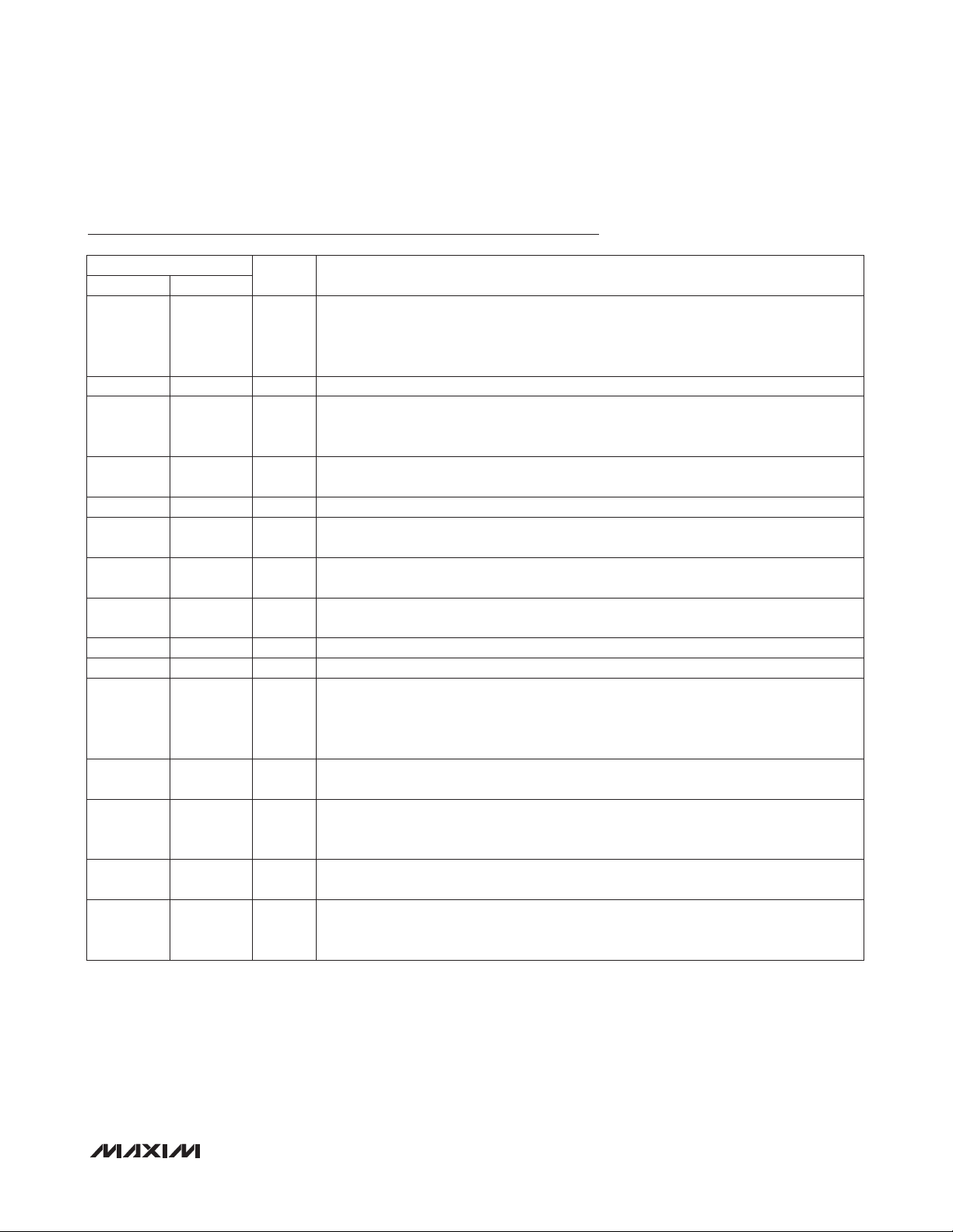
MAX9259 DC ELECTRICAL CHARACTERISTICS
(V
= V
DVDD
Typical values are at V
SINGLE-ENDED INPUTS (DIN_, PCLKIN, PWDN, SSEN, BWS, ES, DRS, MS, CDS, AUTOS, SD, SCK, WS)
High-Level Input Voltage V
Low-Level Input Voltage V
Input Current I
Input Clamp Voltage V
SINGLE-ENDED OUTPUT (INT)
High-Level Output Voltage V
Low-Level Output Voltage V
Output Short-Circuit Current I
2 ______________________________________________________________________________________
= 1.7V to 1.9V, V
AVDD
= V
DVDD
PARAMETER SYMBOL CONDITIONS MIN TYP MAX UNITS
= 1.7V to 3.6V, RL = 100I Q1% (differential), TA = -40NC to +105NC, unless otherwise noted.
IOVDD
AVDD
= V
OH1IOH
= 1.8V, TA = +25NC.)
IOVDD
IH1
IL1
IN1
OL1
OS
VIN = 0 to V
ICL = -18mA -1.5 V
CL
IOL = 2mA 0.2 V
VO = 0V
= -2mA
IOVDD
0.65 x
V
IOVDD
-10 +10
V
IOVDD
- 0.2
V
= 3.0V to 3.6V 16 35 64
IOVDD
V
= 1.7V to 1.9V 3 12 21
IOVDD
0.35 x
V
IOVDD
V
V
FA
V
mA
Page 3
Gigabit Multimedia Serial Link with Spread
Spectrum and Full-Duplex Control Channel
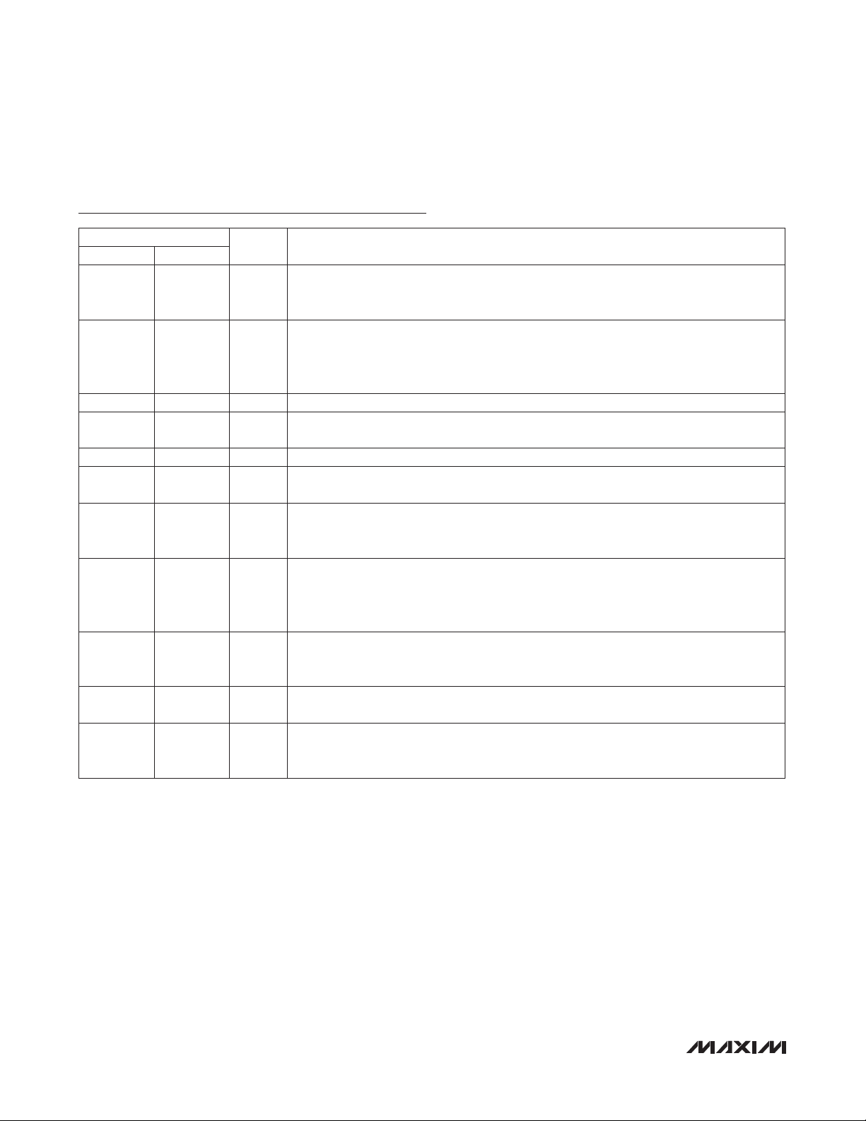
MAX9259 DC ELECTRICAL CHARACTERISTICS (continued)
(V
= V
DVDD
Typical values are at V
I2C AND UART I/O, OPEN-DRAIN OUTPUTS (RX/SDA, TX/SCL, LFLT)
High-Level Input Voltage V
Low-Level Input Voltage V
Input Current I
Low-Level Open-Drain Output
Voltage
DIFFERENTIAL OUTPUT (OUT+, OUT-)
Differential Output Voltage V
Change in VOD Between
Complementary Output States
Output Offset Voltage,
(V
+ + V
OUT
Change in VOS Between
Complementary Output States
Output Short-Circuit Current I
Magnitude of Differential Output
Short-Circuit Current
Output Termination Resistance
(Internal)
REVERSE CONTROL-CHANNEL RECEIVER (OUT+, OUT-)
High Switching Threshold V
Low Switching Threshold V
LINE-FAULT-DETECTION INPUT (LMN_)
Short-to-GND Threshold V
Normal Thresholds V
Open Thresholds V
Open Input Voltage V
Short-to-Battery Threshold V
POWER SUPPLY
Worst-Case Supply Current
(Figure 4)
Sleep-Mode Supply Current I
Power-Down Supply Current I
= 1.7V to 1.9V, V
AVDD
DVDD
= V
= 1.7V to 3.6V, RL = 100I Q1% (differential), TA = -40NC to +105NC, unless otherwise noted.
IOVDD
AVDD
= V
= 1.8V, TA = +25NC.)
IOVDD
PARAMETER SYMBOL CONDITIONS MIN TYP MAX UNITS
IH2
IL2
V
IN2
OL2
VIN = 0 to V
IOL = 3mA
(Note 2) -110 +5
IOVDD
V
= 1.7V to 1.9V 0.4
IOVDD
V
= 3.0V to 3.6V 0.3
IOVDD
Preemphasis off (Figure 1) 300 400 500
OD
3.3dB preemphasis setting, V
(Figure 2)
3.3dB deemphasis setting, V
OD(P)
OD(D)
(Figure 2)
DV
OD
OUT
-)/2 = V
OS
V
DV
I
OSD
R
CHR
CLR
I
WCS
CCS
CCZ
OS
OS
TG
TN
TO
TE
Preemphasis off 1.1 1.4 1.56 V
OS
V
OUT+
V
OUT+
or V
or V
= 0V -60
OUT-
= 1.9V 25
OUT-
VOD = 0V 25 mA
From OUT+, OUT- to V
O
AVDD
Figure 3 0.3 V
Figure 3 0.57 1.07 V
Figure 3 1.45
Figure 3 1.47 1.75 V
IO
Figure 3 2.47 V
f
= 16.6MHz 100 125
PCLKIN
f
= 33.3MHz 105 145
BWS = GND
= GND
PWDN
PCLKIN
f
= 66.6MHz 116 155
PCLKIN
f
= 104MHz 135 175
PCLKIN
0.7 x
V
IOVDD
0.3 x
V
IOVDD
350 610
240 425
15 mV
15 mV
45 54 63
27 mV
-27 mV
VIO+
0.06
40 110
5 70
mV
MAX9259/MAX9260
V
V
FA
V
P-P
mA
I
V
mA
FA
FA
_______________________________________________________________________________________ 3
Page 4
Gigabit Multimedia Serial Link with Spread
Spectrum and Full-Duplex Control Channel
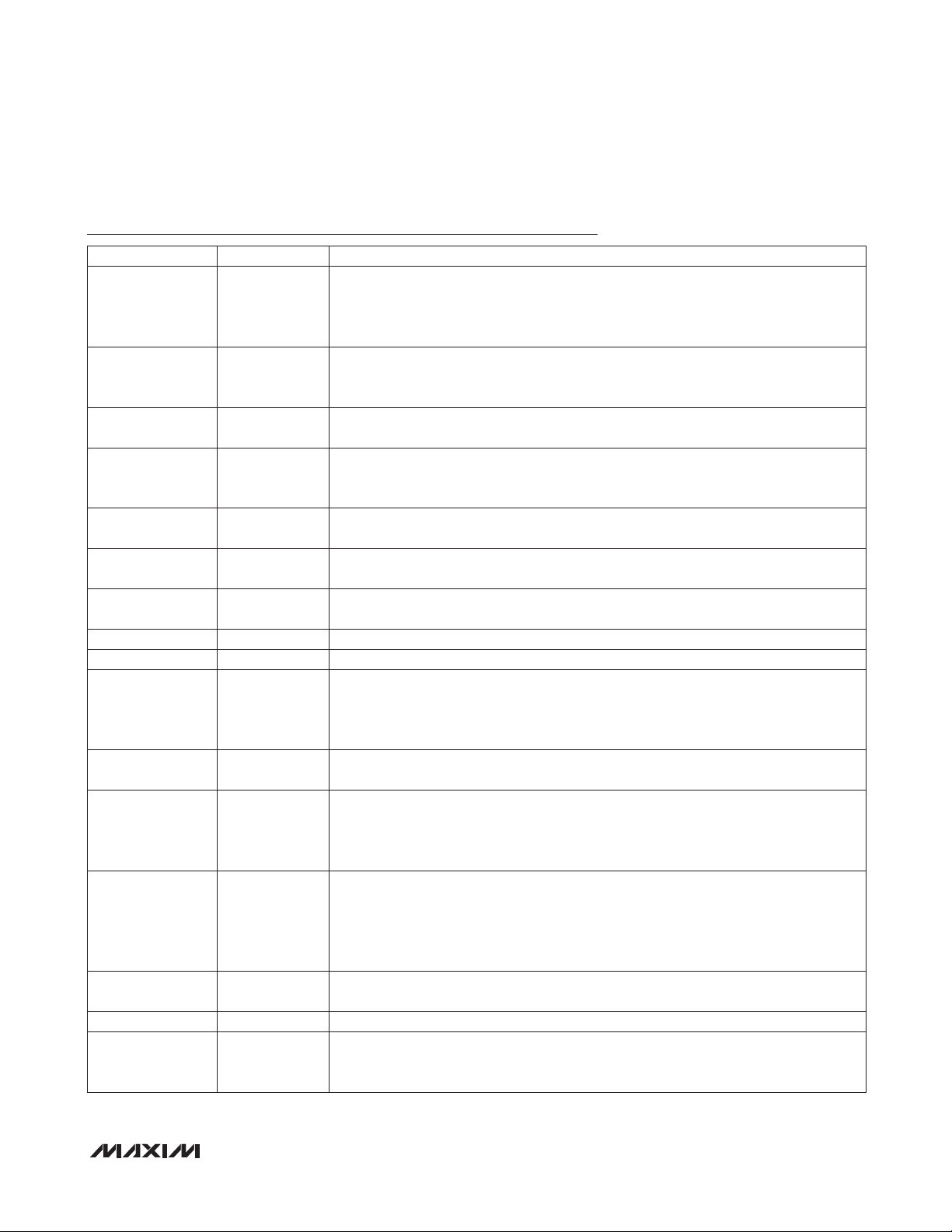
MAX9259 AC ELECTRICAL CHARACTERISTICS
(V
= V
DVDD
Typical values are at V
PARALLEL CLOCK INPUT (PCLKIN)
Clock Frequency f
Clock Duty Cycle DC t
Clock Transition Time tR, t
Clock Jitter t
I2C/UART PORT TIMING (Note 3)
Output Rise Time t
MAX9259/MAX9260
Output Fall Time t
Input Setup Time t
Input Hold Time t
SWITCHING CHARACTERISTICS (Note 3)
Differential Output Rise-and-Fall
Time
Total Serial Output Jitter t
Deterministic Serial Output Jitter t
Parallel Data Input Setup Time t
Parallel Data Input Hold Time t
Serializer Delay (Note 4) t
Link Start Time t
Power-Up Time t
I2S INPUT TIMING
WS Frequency f
Sample Word Length n
SCK Frequency f
SCK Clock High Time (Note 3) t
SCK Clock Low Time (Note 3) t
SD, WS Setup Time t
SD, WS Hold Time t
= 1.7V to 1.9V, V
AVDD
DVDD
= V
= 1.7V to 3.6V, RL = 100I Q1% (differential), TA = -40NC to +105NC, unless otherwise noted.
IOVDD
AVDD
= V
= 1.8V, TA = +25NC.)
IOVDD
PARAMETER SYMBOL CONDITIONS MIN TYP MAX UNITS
V
PCLKIN
F
J
R
F
SET
HOLD
tR, t
F
= V
BWS
V
= V
BWS
V
= V
BWS
V
= V
BWS
HIGH/tT
(Figure 5) 4 ns
3.125Gbps, 300kHz sinusoidal jitter 800 ps
30% to 70%, CL = 10pF to 100pF, 1kI
pullup to IOVDD
70% to 30%, CL = 10pF to 100pF, 1kI
pullup to IOVDD
I2C only (Figure 6) 100 ns
I2C only (Figure 6) 0 ns
20% to 80%, VOD ≥ 400mV, RL = 100I,
serial-data rate = 3.125Gbps
GND
GND
IOVDD
IOVDD
or t
, V
= V
, V
, V
, V
LOW/tT
DRS
DRS
IOVDD
= V
GND
= V
DRS
DRS
= V
IOVDD
GND
(Figure 5) 35 50 65 %
8.33 16.66
16.66 104
6.25 12.5
12.5 78
20 150 ns
20 150 ns
90 150 ps
3.125Gbps PRBS signal, measured at
TSOJ1
VOD = 0V differential, preemphasis
0.25 UI
disabled (Figure 7)
DSOJ2
SET
HOLD
SD
LOCK
PU
WS
WS
SCK
HC
LC
SET
HOLD
3.125Gbps PRBS signal 0.15 UI
(Figure 8) 1 ns
(Figure 8) 1.5 ns
(Figure 9)
Spread spectrum enabled 2830
Spread spectrum disabled 270
(Figure 10) 3.5 ms
(Figure 11) 3.5 ms
(Table 4) 8 192 kHz
(Table 4) 4 32 Bits
f
= fWS x nWS x 2
SCK
V
≥ VIH, t
SCK
V
≤ VIL, t
SCK
SCK
SCK
= 1/f
= 1/f
SCK
SCK
(8 x 4)
x 2
0.35 x
t
SCK
0.35 x
t
SCK
(Figure 12, Note 3) 2 ns
(Figure 12, Note 3) 2 ns
(192 x
32) x 2
MHz
(P-P)
Bits
kHz
ns
ns
4 ______________________________________________________________________________________
Page 5
Gigabit Multimedia Serial Link with Spread
Spectrum and Full-Duplex Control Channel
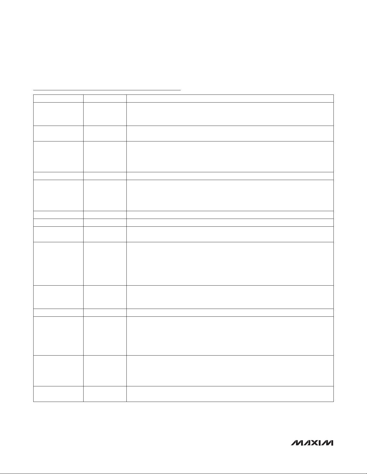
MAX9260 DC ELECTRICAL CHARACTERISTICS
(V
= V
DVDD
Typical values are at V
SINGLE-ENDED INPUTS (ENABLE, INT, PWDN, SSEN, BWS, ES, DRS, MS, CDS, EQS, DCS)
High-Level Input Voltage V
Low-Level Input Voltage V
Input Current I
Input Clamp Voltage V
SINGLE-ENDED OUTPUTS (DOUT_, SD, WS, SCK, PCLKOUT)
High-Level Output Voltage V
Low-Level Output Voltage V
Output Short-Circuit Current I
I2C AND UART I/O, OPEN-DRAIN OUTPUTS (RX/SDA, TX/SCL, ERR, GPIO_, LOCK)
High-Level Input Voltage V
Low-Level Input Voltage V
Input Current I
Low-Level Open-Drain Output
Voltage
= 3.0V to 3.6V, V
AVDD
DVDD
= V
= 1.7V to 3.6V, RL = 100I Q1% (differential), TA = -40NC to +105NC, unless otherwise noted.
IOVDD
AVDD
= V
= 3.3V, TA = +25NC.)
IOVDD
PARAMETER SYMBOL CONDITIONS MIN TYP MAX UNITS
IH1
IL1
IN1
CL
OH
OL1
VIN = 0 to V
IOVDD
ICL = -18mA -1.5 V
V
= V
DCS
IOGND
IOH = -2mA
V
= V
IOL = 2mA
DOUT_,
SD, WS,
SCK
DCS
V
DCS
V
DCS
VO = 0V,
V
= V
DCS
VO = 0V,
V
= V
DCS
= V
= V
IOGND
IOVDD
IOVDD
IOGND
IOVDD
V
3.0V to 3.6V
V
1.7V to 1.9V
V
3.0V to 3.6V
V
IOVDD
IOVDD
IOVDD
IOVDD
=
=
=
=
1.7V to 1.9V
OS
PCLKOUT
VO = 0V,
V
= V
DCS
VO = 0V,
V
= V
DCS
IOGND
IOVDD
V
=
IOVDD
3.0V to 3.6V
V
=
IOVDD
1.7V to 1.9V
V
=
IOVDD
3.0V to 3.6V
V
=
IOVDD
1.7V to 1.9V
IH2
IL2
RX/SDA, TX/SCL -110 +1
GPIO, ERR, LOCK
V
= 1.7V to 1.9V 0.4 V
IOVDD
V
= 3.0V to 3.6V 0.3 V
IOVDD
V
IN2
OL2
VIN = 0 to V
(Note 2)
IOL = 3mA
IOVDD
0.65 x
V
IOVDD
-10 +10
V
IOVDD
- 0.3
V
IOVDD
- 0.2
15 25 39
3 7 13
20 35 63
5 10 21
15 33 50
5 10 17
30 54 97
9 16 32
0.7 x
V
IOVDD
-80 +1
0.35 x
V
IOVDD
0.3
0.2
0.3 x
V
IOVDD
MAX9259/MAX9260
V
V
FA
V
V
mA
V
V
FA
_______________________________________________________________________________________ 5
Page 6
Gigabit Multimedia Serial Link with Spread
Spectrum and Full-Duplex Control Channel
MAX9260 DC ELECTRICAL CHARACTERISTICS (continued)
(V
= V
DVDD
Typical values are at V
DIFFERENTIAL OUTPUTS FOR REVERSE CONTROL CHANNEL (IN+, IN-)
Differential High Output Peak
Voltage, (VIN+) - (VIN-)
Differential Low Output Peak
Voltage, (VIN+) - (VIN-)
DIFFERENTIAL INPUTS (IN+, IN-)
Differential High Input Threshold
(Peak), (VIN+) - (VIN-)
Differential Low Input Threshold
(Peak), (VIN+) - (VIN-)
Input Common-Mode Voltage,
MAX9259/MAX9260
((VIN+) + (VIN-))/2
Differential Input Resistance
(Internal)
POWER SUPPLY
Worst-Case Supply Current
(Figure 15)
Sleep-Mode Supply Current I
Power-Down Supply Current I
= 3.0V to 3.6V, V
AVDD
= V
DVDD
PARAMETER SYMBOL CONDITIONS MIN TYP MAX UNITS
= 1.7V to 3.6V, RL = 100I Q1% (differential), TA = -40NC to +105NC, unless otherwise noted.
IOVDD
AVDD
= V
V
ROH
V
ROL
V
IDH(P)
V
IDL(P)
V
CMR
I
WCS
CCS
CCZ
= 3.3V, TA = +25NC.)
IOVDD
No high-speed data transmission
(Figure 13)
No high-speed data transmission
(Figure 13)
(Figure 14) 40 90 mV
(Figure 14) -90 -40 mV
R
I
V
BWS
f
PCLKOUT
V
BWS
f
PCLKOUT
V
BWS
f
PCLKOUT
V
BWS
f
PCLKOUT
V
PWDN
= V
IOGND
= 16.6MHz
= V
IOGND
= 33.3MHz
= V
IOGND
= 66.6MHz
= V
IOGND
= 104MHz
= V
IOGND
2% spread
spectrum active
,
Spread spectrum
disabled
2% spread
spectrum active
,
Spread spectrum
disabled
2% spread
spectrum active
,
Spread spectrum
disabled
2% spread
spectrum active
,
Spread spectrum
disabled
30 60 mV
-60 -30 mV
1 1.3 1.6 V
80 100 130
113 166
105 155
122 181
110 165
137 211
120 188
159 247
135 214
80 130
19 70
I
mA
FA
FA
6 ______________________________________________________________________________________
Page 7
Gigabit Multimedia Serial Link with Spread
Spectrum and Full-Duplex Control Channel
MAX9260 AC ELECTRICAL CHARACTERISTICS
(V
= V
DVDD
Typical values are at V
PARALLEL CLOCK OUTPUT (PCLKOUT)
Clock Frequency f
Clock Duty Cycle DC t
Clock Jitter t
I2C/UART PORT TIMING
Output Rise Time t
Output Fall Time t
Input Setup Time t
Input Hold Time t
SWITCHING CHARACTERISTICS
PCLKOUT Rise-and-Fall Time tR, t
Parallel Data Rise-and-Fall Time
(Figure 17)
Deserializer Delay t
Lock Time t
Power-Up Time t
Reverse Control-Channel Output
Rise Time
Reverse Control-Channel Output
Fall Time
= 3.0V to 3.6V, V
AVDD
DVDD
= V
= 1.7V to 3.6V, RL = 100I Q1% (differential), TA = -40NC to +105NC, unless otherwise noted.
IOVDD
AVDD
= V
= 3.3V, TA = +25NC.)
IOVDD
PARAMETER SYMBOL CONDITIONS MIN TYP MAX UNITS
V
PCLKOUT
J
R
F
SET
HOLD
= V
BWS
V
= V
BWS
V
= V
BWS
V
= V
BWS
or t
HIGH/tT
Period jitter, RMS, spread off, 3.125Gbps,
PRBS pattern, UI = 1/f
30% to 70%, CL = 10pF to 100pF, 1kI
pullup to IOVDD
70% to 30%, CL = 10pF to 100pF, 1kI
pullup to IOVDD
I2C only 100 ns
I2C only 0 ns
IOGND
IOGND
IOVDD
IOVDD
LOW/tT
, V
DRS
, V
DRS
, V
DRS
, V
DRS
(Figure 16) 40 50 60 %
20% to 80%,
V
= 1.7V to 1.9V
IOVDD
F
20% to 80%,
V
= 3.0V to 3.6V
IOVDD
20% to 80%,
V
= 1.7V to 1.9V
IOVDD
tR, t
F
20% to 80%,
V
= 3.0V to 3.6V
IOVDD
SD
LOCK
PU
t
t
Spread spectrum enabled (Figure 18) 2880
Spread spectrum disabled (Figure 18) 750
Spread spectrum enabled (Figure 19) 1500
Spread spectrum off (Figure 19) 1000
(Figure 20) 2500
No high-speed transmission (Figure 13) 180 400 ns
R
No high-speed transmission (Figure 13) 180 400 ns
F
= V
IOVDD
= V
IOGND
= V
IOVDD
= V
IOGND
PCLKOUT
V
DCS
CL = 10pF
V
DCS
CL = 5pF
V
DCS
CL = 10pF
V
DCS
CL = 5pF
V
DCS
CL = 10pF
V
DCS
CL = 5pF
V
DCS
CL = 10pF
V
DCS
CL = 5pF
= V
= V
= V
= V
= V
= V
= V
= V
IOVDD
IOGND
IOVDD
IOGND
IOVDD
IOGND
IOVDD
IOGND
8.33 16.66
16.66 104
6.25 12.5
12.5 78
0.05 UI
20 150 ns
20 150 ns
,
0.4 2.2
,
0.5 2.8
,
0.25 1.7
,
0.3 2.0
,
0.5 3.1
,
0.6 3.8
,
0.3 2.2
,
0.4 2.4
MAX9259/MAX9260
MHz
ns
ns
Bits
Fs
Fs
_______________________________________________________________________________________ 7
Page 8

Gigabit Multimedia Serial Link with Spread
Spectrum and Full-Duplex Control Channel
MAX9260 AC ELECTRICAL CHARACTERISTICS (continued)
(V
= V
DVDD
Typical values are at V
I2S OUTPUT TIMING
WS Jitter t
SCK Jitter t
MAX9259/MAX9260
Audio Skew Relative to Video
SCK, SD, WS Rise-and-Fall Time tR, t
SD, WS Valid Time Before SCK t
SD, WS Valid Time After SCK t
= 3.0V to 3.6V, V
AVDD
DVDD
= V
= 1.7V to 3.6V, RL = 100I Q1% (differential), TA = -40NC to +105NC, unless otherwise noted.
IOVDD
AVDD
= V
= 3.3V, TA = +25NC.)
IOVDD
PARAMETER SYMBOL CONDITIONS MIN TYP MAX UNITS
AJ-WS
AJ-SCK
ASK
F
DVB
DVA
fWS = 48kHz or
tWS = 1/fWS, rising
44.1kHz
(falling) edge to
falling (rising) edge
(Note 5)
fWS = 192kHz
nWS = 16 bits,
fWS = 48kHz or 44.1kHz
t
= 1/f
SCK
edge to rising edge
SCK
, rising
nWS = 24 bits,
fWS = 96kHz
nWS = 32 bits,
fWS = 192kHz
Video and audio synchronized 3 x tWS4 x t
V
20% to 80%
t
= 1/f
SCK
t
SCK
= 1/f
SCK
SCK
= V
DCS
V
= V
DCS
(Figure 21)
(Figure 21)
, CL = 10pF 0.3 3.1 ns
IOVDD
, CL = 5pF 0.4 3.8 ns
IOGND
x t
x t
0.35
SCK
0.35
SCK
0.4e - 3
x t
WS
0.8e - 3
x t
WS
1.6e - 3
x t
WS
13e - 3
x t
SCK
39e - 3
x t
SCK
0.1
x t
SCK
0.5
x t
SCK
0.5
x t
SCK
0.5e - 3
x t
WS
1e - 3
x t
WS
2e - 3
x t
WS
16e - 3
x t
SCK
48e - 3
x t
SCK
0.13
x t
SCK
WS
nsfWS = 96kHz
ns
µs
ns
ns
Note 2: Minimum IIN due to voltage drop across the internal pullup resistor.
Note 3: Not production tested.
Note 4: Bit time = 1/(30 x f
RXCLKIN
) (BWS = 0), = 1/(40 x f
RXCLKIN
) (BWS = V
IOVDD
).
Note 5: Rising to rising edge jitter can be twice as large.
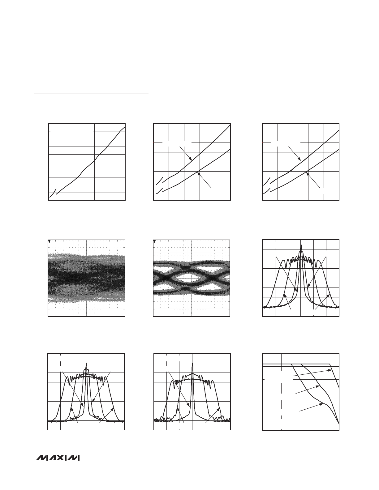
Typical Operating Characteristics
(V
= V
DVDD
vs. PCLKIN FREQUENCY (24-BIT MODE)
135
130
125
120
115
110
105
SUPPLY CURRENT (mA)
100
95
90
5 105
8 ______________________________________________________________________________________
AVDD
= V
= 1.8V (MAX9259), V
IOVDD
MAX9259 SUPPLY CURRENT
PREEMPHASIS =
0x0B TO 0x0F
PREEMPHASIS =
0x01 TO 0x04
PREEMPHASIS = 0x00
PCLKIN FREQUENCY (MHz)
= V
DVDD
vs. PCLKIN FREQUENCY (32-BIT MODE)
135
130
125
MAX9259/60 toc01
120
115
110
105
SUPPLY CURRENT (mA)
100
95
85654525
90
5 80
AVDD
= V
= 3.3V (MAX9260), TA = +25NC, unless otherwise noted.)
IOVDD
MAX9259 SUPPLY CURRENT
PREEMPHASIS =
0x0B TO 0x0F
PREEMPHASIS =
0x01 TO 0x04
PREEMPHASIS = 0x00
65503520
PCLKIN FREQUENCY (MHz)
155
150
145
MAX9259/60 toc02
140
135
130
125
120
SUPPLY CURRENT (mA)
115
110
105
MAX9260 SUPPLY CURRENT
vs. PCLKOUT FREQUENCY (24-BIT MODE)
ALL EQUALIZER SETTINGS
5 105
PCLKOUT FREQUENCY (MHz)
85654525
MAX9259/60 toc03
Page 9
Gigabit Multimedia Serial Link with Spread
OUTPUT POWER SPECTRUM
Spectrum and Full-Duplex Control Channel
Typical Operating Characteristics (continued)
(V
DVDD
= V
AVDD
= V
= 1.8V (MAX9259), V
IOVDD
DVDD
= V
AVDD
= V
= 3.3V (MAX9260), TA = +25NC, unless otherwise noted.)
IOVDD
MAX9259/MAX9260
MAX9260 SUPPLY CURRENT
vs. PCLKOUT FREQUENCY (32-BIT MODE)
155
ALL EQUALIZER SETTINGS
150
145
140
135
130
125
120
SUPPLY CURRENT (mA)
115
110
105
5 80
PCLKOUT FREQUENCY (MHz)
65503520
SERIAL LINK SWITCHING PATTERN
WITHOUT PREEMPHASIS
(PARALLEL BIT RATE = 104MHz, 10m STP CABLE)
400.0mV 3.12Gbps
-400.0mV 52.00ps/div
MAX9259/60 toc07
OUTPUT POWER SPECTRUM
vs. PCLKOUT FREQUENCY
(MAX9259 SPREAD ON, MAX9260 SPREAD OFF)
0
f
= 42MHz
PCLKOUT
-10
0% SPREAD
-20
-30
-40
-50
-60
PCLKOUT OUTPUT POWER (dBm)
-70
-80
2% SPREAD
39 45
PCLKOUT FREQUENCY (MHz)
0.5% SPREAD
4% SPREAD
444340 41 42
MAX9260 SUPPLY CURRENT
vs. PCLKOUT FREQUENCY (24-BIT MODE)
180
170
MAX9259/60 toc04
160
150
140
130
SUPPLY CURRENT (mA)
120
110
100
2%, 4% SPREAD
NO SPREAD
5 105
PCLKOUT FREQUENCY (MHz)
SERIAL LINK SWITCHING PATTERN
WITH 14dB PREEMPHASIS
(PARALLEL BIT RATE = 104MHz, 10m STP CABLE)
250.0mV
-250.0mV 52.00ps/div
OUTPUT POWER SPECTRUM
vs. PCLKOUT FREQUENCY
(MAX9260 SPREAD ON, MAX9259 SPREAD OFF)
0
f
= 42MHz
PCLKOUT
-10
MAX9259/60 toc10
0% SPREAD
-20
-30
-40
-50
-60
PCLKOUT OUTPUT POWER (dBm)
-70
-80
2% SPREAD
39 45
PCLKOUT FREQUENCY (MHz)
4% SPREAD
856525 45
MAX9259/60 toc08
3.12Gbps
444340 41 42
vs. PCLKOUT FREQUENCY (32-BIT MODE)
180
170
MAX9259/60 toc05
160
150
140
130
SUPPLY CURRENT (mA)
120
110
100
5 80
(MAX9259 SPREAD ON, MAX9260 SPREAD OFF)
0
-10
-20
-30
-40
-50
-60
PCLKOUT OUTPUT POWER (dBm)
-70
-80
18.5 21.5
120
MAX9259/60 toc11
100
80
60
FREQUENCY (MHz)
40
20
0
0 20
MAX9260 SUPPLY CURRENT
2%, 4% SPREAD
NO SPREAD
655020 35
PCLKOUT FREQUENCY (MHz)
vs. PCLKOUT FREQUENCY
f
= 20MHz
PCLKOUT
0% SPREAD 0.5% SPREAD
4% SPREAD2% SPREAD
21.020.519.0 19.5 20.0
PCLKOUT FREQUENCY (MHz)
MAXIMUM PCLKIN FREQUENCY vs.
STP CABLE LENGTH (BER < 10
OPTIMUM PE/EQ
SETTINGS
NO PE, EQS = LOW
NO PE, EQS = HIGH
BER CAN BE < 10
CABLE LENGTHS LESS THAN 10m
-12
FOR
CABLE LENGTH (m)
-9
15105
MAX9259/60 toc06
MAX9259/60 toc09
)
MAX9259/60 toc12
_______________________________________________________________________________________ 9
Page 10

Gigabit Multimedia Serial Link with Spread
Spectrum and Full-Duplex Control Channel
Pin Configurations
TOP VIEW
DRS
INT
LMN0
AVDD
OUT+
OUT-
AGND
LMN1
SSEN
DIN17
DIN18
TX/SCL
DIN19
RX/SDA
DIN20
BWS
48
49
50
GND
51
IOVDD
DIN1
52
53
DIN2
54
DIN3
DIN4
55
DIN5
56
DIN6
57
DIN7
58
59
DIN8
60
DIN9
MAX9259/MAX9260
GND
DVDD
DIN10
DIN11
61
62
63
64
DIN12
ES
DIN13
EP*
DIN14
DIN15
LFLT
DIN16
PCLKIN
MAX9259
GND
IOVDD
TQFP
AGND
38394041424344454647
111098765432 16151413121
AVDD
(10mm × 10mm × 1mm)
PWDN
3334353637
DIN21
CDS
DIN22
TOP VIEW
DOUT11
DOUT12
DOUT14
DOUT15
PCLKOUT
DOUT16
DOUT17
DOUT18
DOUT19
DOUT21
DOUT22
DOUT9
48
32
MSDIN0
31
GND
30
IOVDD
29
AUTOS
28
WS
27
SCK
SD
26
25
DIN28
24
DIN27
23
DIN26
22
DIN25
21
DIN24
20
GND
19
DVDD
18
AGND
17
DIN23
IOGND
IOVDD
DOUT7
DOUT6
DOUT5
DOUT4
DOUT3
DOUT2
DOUT1
DOUT0
IOGND
SSEN
DRS
AVDD
AGND
49
50
51
52
53
54
55
56
57
58
59
60
61
62
63
64
ENABLE
DOUT10
INT
BWS
DOUT13
38394041424344454647
MAX9260
EP*
111098765432 16151413121
ES
IN-
IN+
CDS
GPIO0
AVDD
AGND
EQS
GPIO1
TQFP
DOUT20
MS
DCS
DVDD
3334353637
DOUT23
DGND
32
DOUT24DOUT8
31
IOGND
30
IOVDD
29
DOUT25
28
DOUT26
27
DOUT27
DOUT28/MCLK
26
25
SD
24
SCK
23
WS
22
LOCK
21
IOGND
20
ERR
19
PWDN
18
TX/SCL
17
RX/SDA
(10mm × 10mm × 1mm)
TOP VIEW
TX/SCL
RX/SDA
EP*
DIN20
DIN21
PWDN
DIN22
28
CDS
27
MS
26
IOVDD
25
AUTOS
24
WS
23
SCK
22
SD
21
DIN28
20
DIN27
19
DIN26
18
DIN25
17
DIN24
16
DVDD
15
DIN23
DRS
ES
BWS
42 41 40 39 38 37 36 35 34 33 32 31 30 29
DIN0
43
IOVDD
44
DIN1
45
DIN2
46
DIN3
47
DIN4
48
DIN5
49
DIN6
50
DIN7
51
52
DIN8
53
DIN9
54
DVDD
55
DIN10
DIN11
*CONNECT EP TO GROUND PLANE
+
56
1 2
3 4 5 6 7 8 9 10 11 12 13 14
DIN14
DIN13
DIN12
LMN1
OUT-
OUT+
AVDD
LMN0
LFLT
INT
MAX9259
AVDD
DIN18
IOVDD
TQFN
DIN17
DIN16
DIN15
PCLKIN
(8mm x 8mm x 0.75mm)
SSEN
DIN19
10 _____________________________________________________________________________________
Page 11
Gigabit Multimedia Serial Link with Spread
Spectrum and Full-Duplex Control Channel
MAX9259 Pin Description
MAX9259/MAX9260
PIN
TQFP TQFN
1–5, 11–17,
21–25, 49,
52–60, 63,
64
6 6 PCLKIN Parallel Clock Input. Latches parallel data inputs and provides the PLL reference clock.
7, 30, 51 7, 26, 44 IOVDD
8, 20, 31,
50, 61
9, 18, 39 — AGND Analog Ground
10, 42 8, 36 AVDD
19, 62 16, 54 DVDD
26 22 SD
27 23 SCK I2S Serial-Clock Input with Internal Pulldown to GND
28 24 WS I2S Word-Select Input with Internal Pulldown to GND
29 25
32 27 MS
33 28 CDS
34 29
35 30 RX/SDA
1–5, 9–15,
17–21, 43,
45–53, 55,
56
— GND Digital and I/O Ground
NAME FUNCTION
Data Input[0:28]. Parallel data inputs. All pins internally pulled down to GND. Selected
DIN0–
DIN28
AUTOS
PWDN
edge of PCLKIN latches input data. Set BWS = low (24-bit mode) to use DIN0–DIN20
(RGB and SYNC). DIN21–DIN28 are not used in 24-bit mode. Set BWS = high (32-bit
mode) to use DIN0–DIN28 (RGB, SYNC, and two extra inputs).
I/O Supply Voltage. 1.8V to 3.3V logic I/O power supply. Bypass IOVDD to GND with
0.1FF and 0.001FF capacitors as close as possible to the device with the smaller value
capacitor closest to IOVDD.
1.8V Analog Power Supply. Bypass AVDD to AGND with 0.1FF and 0.001FF capacitors as
close as possible to the device with the smaller value capacitor closest to AVDD.
1.8V Digital Power Supply. Bypass DVDD to GND with 0.1FF and 0.001FF capacitors as
close as possible to the device with the smaller value capacitor closest to DVDD.
I2S Serial-Data Input with Internal Pulldown to GND. Disable I2S to use SD as an
additional data input latched on the selected edge of PCLKIN.
Autostart Setting. Active-low power-up mode selection input requires external pulldown or
pullup resistors. Set AUTOS = high to power up the device with no link active. Set AUTOS
= low to have the MAX9259 power up the serial link with autorange detection (see Tables
13 and 14).
Mode Select. Control-link mode-selection input requires external pulldown or pullup
resistors. Set MS = low, to select base mode. Set MS = high to select the bypass mode.
Control-Direction Selection. Control-link-direction selection input requires external
pulldown or pullup resistors. Set CDS = low for FC use on the MAX9259 side of the serial
link. Set CDS = high for FC use on the MAX9260 side of the serial link.
Power-Down. Active-low power-down input requires external pulldown or pullup
resistors.
Receive/Serial Data. UART receive or I2C serial-data input/output with internal 30kI
pullup to IOVDD. In UART mode, RX/SDA is the Rx input of the MAX9259’s UART. In I2C
mode, RX/SDA is the SDA input/output of the MAX9259’s I2C master.
______________________________________________________________________________________ 11
Page 12
Gigabit Multimedia Serial Link with Spread
Spectrum and Full-Duplex Control Channel
MAX9259 Pin Description (continued)
PIN
TQFP TQFN
36 31 TX/SCL
37 32 SSEN
38 33 LMN1 Line-Fault Monitor Input 1 (see Figure 3 for details)
40, 41
43 37 LMN0 Line-Fault Monitor Input 0 (see Figure 3 for details)
MAX9259/MAX9260
44 38 LFLT
45 39 INT
46 40 DRS
47 41 ES
48 42 BWS
— — EP
34, 35
NAME FUNCTION
Transmit/Serial Clock. UART transmit or I2C serial-clock output with internal 30kI
pullup to IOVDD. In UART mode, TX/SCL is the Tx output of the MAX9259’s UART. In I2C
mode, TX/SCL is the SCL output of the MAX9259’s I2C master.
Spread-Spectrum Enable. Serial link spread-spectrum enable input requires external
pulldown or pullup resistors. The state of SSEN latches upon power-up or when resuming
from power-down mode (PWDN = low). Set SSEN = high for Q0.5% spread spectrum on
the serial link. Set SSEN = low to use the serial link without spread spectrum.
OUT-,
OUT+
Differential CML Output -/+. Differential outputs of the serial link.
Line Fault. Active-low open-drain line-fault output with a 60kI internal pullup resistor.
LFLT = low indicates a line fault. LFLT is high impedance when PWDN = low.
Interrupt Output to Indicate Remote Side Requests. INT = low upon power-up and when
PWDN = low. A transition on the INT input of the MAX9260 toggles the MAX9259’s INT
output.
Data-Rate Select. Data-rate range-selection input requires external pulldown or pullup
resistors. Set DRS = high for parallel input data rates of 8.33MHz to 16.66MHz (24-bit
mode) or 6.25MHz to 12.5MHz (32-bit mode). Set DRS = low for parallel input data rates
of 16.66MHz to 104MHz (24-bit mode) or 12.5MHz to 78MHz (32-bit mode).
Edge Select. PCLKIN trigger edge-selection input requires external pulldown or pullup
resistors. Set ES = low to trigger on the rising edge of PCLKIN. Set ES = high to trigger on
the falling edge of PCLKIN.
Bus-Width Select. Parallel input bus-width selection input requires external pulldown or
pullup resistors. Set BWS = low for 24-bit bus mode. Set BWS = high for 32-bit bus mode.
Exposed Pad. EP internally connected to AGND (TQFP package) or AGND and GND
(TQFN package). MUST externally connect EP to the AGND plane to maximize thermal
and electrical performance.
12 _____________________________________________________________________________________
Page 13
Gigabit Multimedia Serial Link with Spread
Spectrum and Full-Duplex Control Channel
MAX9260 Pin Description
PIN NAME FUNCTION
Enable. Active-low parallel output-enable input requires external pulldown or pullup
1
2 BWS
3 INT
4 CDS
5 GPIO0
6 ES
7, 63 AVDD
8 , 9 IN+, IN- Differential CML Input +/-. Differential inputs of the serial link.
10, 64 AGND Analog Ground
11 EQS
12 GPIO1
13 DCS
ENABLE
resistors. Set ENABLE = low to enable PCLKOUT, SD, SCK, WS, and the parallel outputs, DOUT_. Set ENABLE = high to put PCLKOUT, SD, SCK, WS, and DOUT_ to high
impedance.
Bus-Width Select. Parallel output bus-width selection input requires external pulldown
or pullup resistors. Set BWS = low for 24-bit bus mode. Set BWS = high for 32-bit bus
mode.
Interrupt. Interrupt input requires external pulldown or pullup resistors. A transition on
the INT input of the MAX9260 toggles the MAX9259’s INT output.
Control-Direction Selection. Control-link-direction selection input requires external pulldown or pullup resistors. Set CDS = low for FC use on the MAX9259 side of the serial
link. Set CDS = high for FC use on the MAX9260 side of the serial link.
GPIO0. Open-drain general-purpose input/output with internal 60kI pullup resistors to
IOVDD. GPIO0 is high impedance during power-up and when PWDN = low.
Edge Select. PCLKOUT edge-selection input requires external pulldown or pullup
resistors. Set ES = low for a rising-edge trigger. Set ES = high for a falling-edge trigger.
3.3V Analog Power Supply. Bypass AVDD to AGND with 0.1µF and 0.001µF capacitors
as close as possible to the device with the smallest value capacitor closest to AVDD.
Equalizer Select. Deserializer equalizer-selection input requires external pulldown or
pullup resistors. The state of EQS latches upon power-up or rising edge of PWDN. Set
EQS = low for 10.7dB equalizer boost (EQTUNE = 1001). Set EQS = high for 5.2dB
equalizer boost (EQTUNE = 0100).
GPIO1. Open-drain general-purpose input/output with internal 60kI pullup resistors to
IOVDD. GPIO1 is high impedance during power-up and when PWDN = low.
Drive Current Select. Driver current-selection input requires external pulldown or pullup resistors. Set DCS = high for stronger parallel data and clock output drivers. Set
DCS = low for normal parallel data and clock drivers (see the MAX9260 DC Electrical
Characteristics table).
MAX9259/MAX9260
Mode Select. Control-link mode-selection/autostart mode selection input requires
external pulldown or pullup resistors. MS sets the control-link mode when CDS = high
14 MS
15 DVDD
16 DGND Digital Ground
17 RX/SDA
______________________________________________________________________________________ 13
(see the Control-Channel and Register Programming section). Set MS = low to select
base mode. Set MS = high to select the bypass mode. MS sets autostart mode when
CDS = low (see Tables 13 and 14).
3.3V Digital Power Supply. Bypass DVDD to DGND with 0.1FF and 0.001FF capacitors
as close as possible to the device with the smaller value capacitor closest to DVDD.
Receive/Serial Data. UART receive or I2C serial-data input/output with internal 30kI
pullup to IOVDD. In UART mode, RX/SDA is the Rx input of the MAX9260’s UART. In
I2C mode, RX/SDA is the SDA input/output of the MAX9259’s I2C master.
Page 14
Gigabit Multimedia Serial Link with Spread
Spectrum and Full-Duplex Control Channel
MAX9260 Pin Description (continued)
PIN NAME FUNCTION
Transmit/Serial Clock. UART transmit or I2C serial-clock output with internal 30kI
18 TX/SCL
19
20
21, 31, 50, 60 IOGND Input/Output Ground
22 LOCK
PWDN
ERR
MAX9259/MAX9260
23 WS Word Select. I2S word-select output.
24 SCK Serial Clock. I2S serial-clock output
25 SD
26–29, 32–40,
42–49, 52–59
DOUT0–
DOUT27,
DOUT28/MCLK
pullup to IOVDD. In UART mode, TX/SCL is the Tx output of the MAX9259’s UART. In
I2C mode, TX/SCL is the SCL output of the MAX9260’s I2C master.
Power-Down. Active-low power-down input requires external pulldown or pullup resistors.
Error. Active-low open-drain video data error output with internal pullup to IOVDD.
ERR goes low when the number of decoding errors during normal operation exceed a
programmed error threshold or when at least one PRBS error is detected during PRBS
test. ERR is high impendence when PWDN = low.
Open-Drain Lock Output with Internal Pullup to IOVDD. LOCK = high indicates PLLs
are locked with correct serial-word-boundary alignment. LOCK = low indicates PLLs
are not locked or incorrect serial-word-boundary alignment. LOCK remains low when
the configuration link is active. LOCK is high impedance when PWDN = low.
Serial Data. I2S serial-data output. Disable I2S to use SD as an additional data output
latched on the selected edge of PCLKOUT.
Data Output[0:28]. Parallel data outputs. Output data can be strobed on the selected
edge of PCLKOUT. Set BWS = low (24-bit mode) to use DOUT0–DOUT20 (RGB and
SYNC). DOUT21–DOUT28 are not used in 24-bit mode and are set to low. Set BWS =
high (32-bit mode) to use DOUT0–DOUT28 (RGB, SYNC, and two extra outputs).
DOUT28 can be used to output MCLK (see the Additional MCLK Output for Audio
Applications section).
1.8V to 3.3V Logic I/O Power Supply. Bypass IOVDD to IOGND with 0.1FF and 0.001FF
30, 51 IOVDD
41 PCLKOUT Parallel Clock Output. Used for DOUT0–DOUT28.
61 SSEN
62 DRS
— EP
14 _____________________________________________________________________________________
capacitors as close as possible to the device with the smaller value capacitor closest
to IOVDD.
Spread-Spectrum Enable. Parallel output spread-spectrum enable input requires
external pulldown or pullup resistors. The state of SSEN latches upon power-up or
when resuming from power-down mode (PWDN = low). Set SSEN = high for Q2%
spread spectrum on the parallel outputs. Set SSEN = low to use the parallel outputs
without spread spectrum.
Data-Rate Select. Data-rate range-selection input requires external pulldown or pullup
resistors. Set DRS = high for parallel input data rates of 8.33MHz to 16.66MHz (24-bit
mode) or 6.25MHz to 12.5MHz (32-bit mode). Set DRS = low for parallel input data
rates of 16.66MHz to 104MHz (24-bit mode) or 12.5MHz to 78MHz (32-bit mode).
Exposed Pad. EP internally connected to AGND. MUST externally connect EP to the
AGND plane to maximize thermal and electrical performance.
Page 15
Gigabit Multimedia Serial Link with Spread
Spectrum and Full-Duplex Control Channel
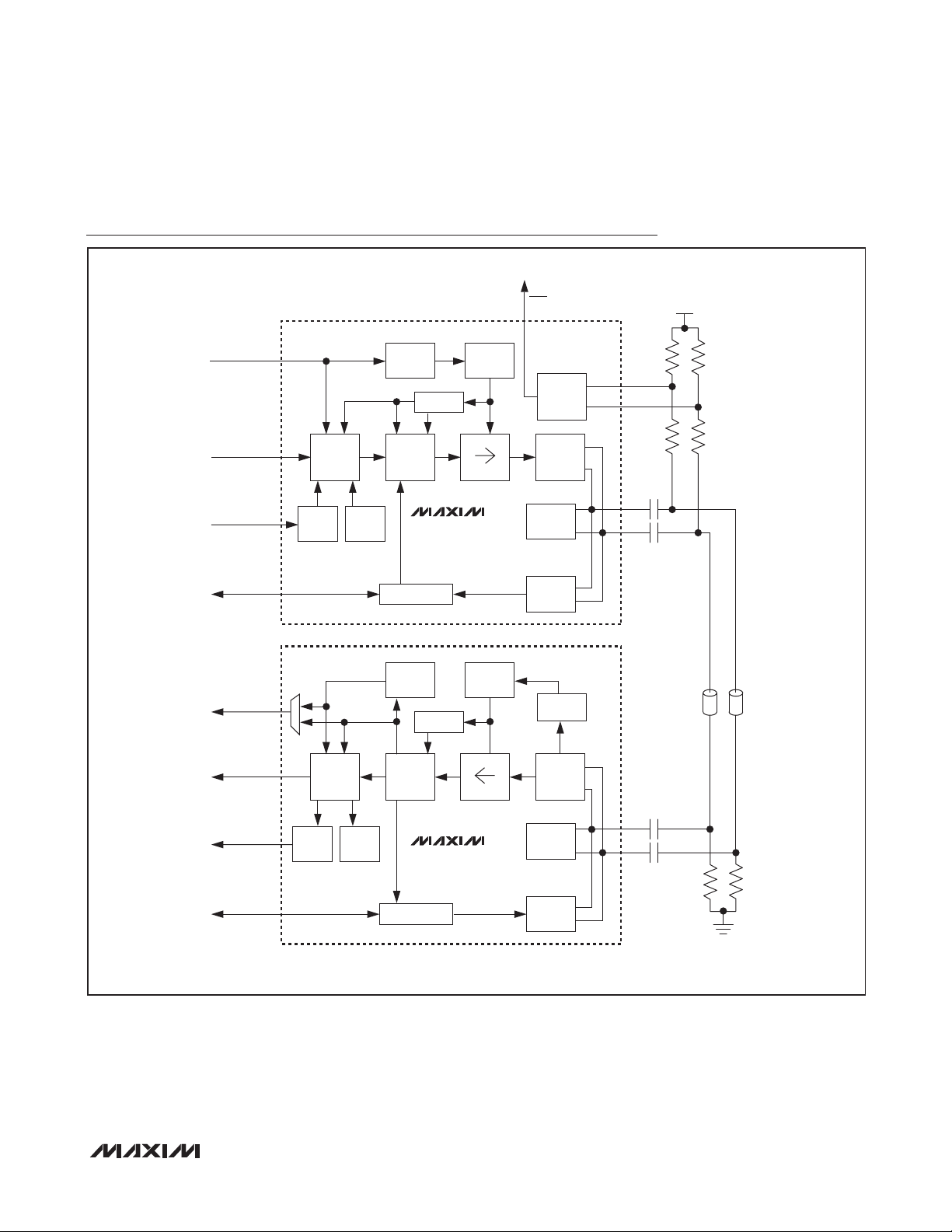
Functional Diagram
LFLT
MAX9259/MAX9260
PCLKIN
DIN[N:0]
WS, SD, SCK
TX/SCL
RX/SDA
PCLKOUT
DOUT[N:0]
AUDIO
FIFO
FIFO
FIFO
PRBS
GEN
FILTER
PLL
8B/10B
ENCODE
PARITY
UART/I2C
SPREAD
PLL
8B/10B
DECODE
PARITY
CLKDIV
MAX9259
SERIALIZER
CLKDIV
SPREAD
PLL
P S
CDR
PLL
P S
LINE-
FAULT
CML
TERM
REV CH
Rx
CML
DET
Tx
EQ
Rx
LMN0
LMN1
OUT+
OUT-
STP CABLE
= 50)
(Z
0
WS, SD, SCK
TX/SCL
RX/SDA
AUDIO
FIFO
PRBS
CHECK
UART/I2C
TERM
MAX9260
REV CH
Tx
DESERIALIZER
IN-
IN+
______________________________________________________________________________________ 15
Page 16
Gigabit Multimedia Serial Link with Spread
Spectrum and Full-Duplex Control Channel
/2
R
V
= |V
L
OD
V
GND
OS
V
OS(-)
V
OS(+)
OS(+)
R
- V
/2
L
((OUT+) + (OUT-))/2
|
OS(-)
OUT-
OUT+
V
OS(-)
OUT+
OUT-
DV
OS
MAX9259/MAX9260
V
OD(-)
(OUT+) - (OUT-)
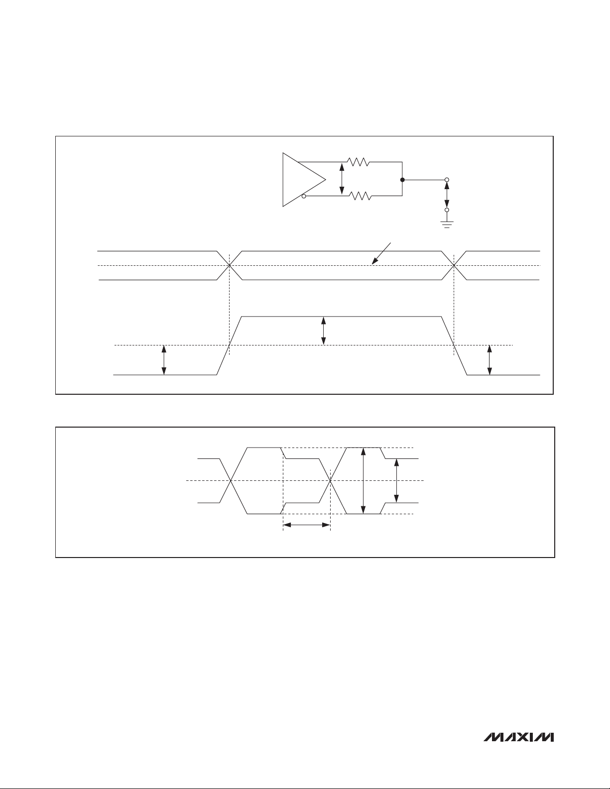
Figure 1. MAX9259 Serial Output Parameters
OUT+
V
OS
OUT-
Figure 2. Output Waveforms at OUT+ and OUT-
SERIAL-BIT
TIME
VOD(+)
DVOD = |V
OD(+)
- V
OD(-)
V
|
OD(P)VOD(D)
V
OD(-)
V
= 0V
OD
16 _____________________________________________________________________________________
Page 17
Gigabit Multimedia Serial Link with Spread
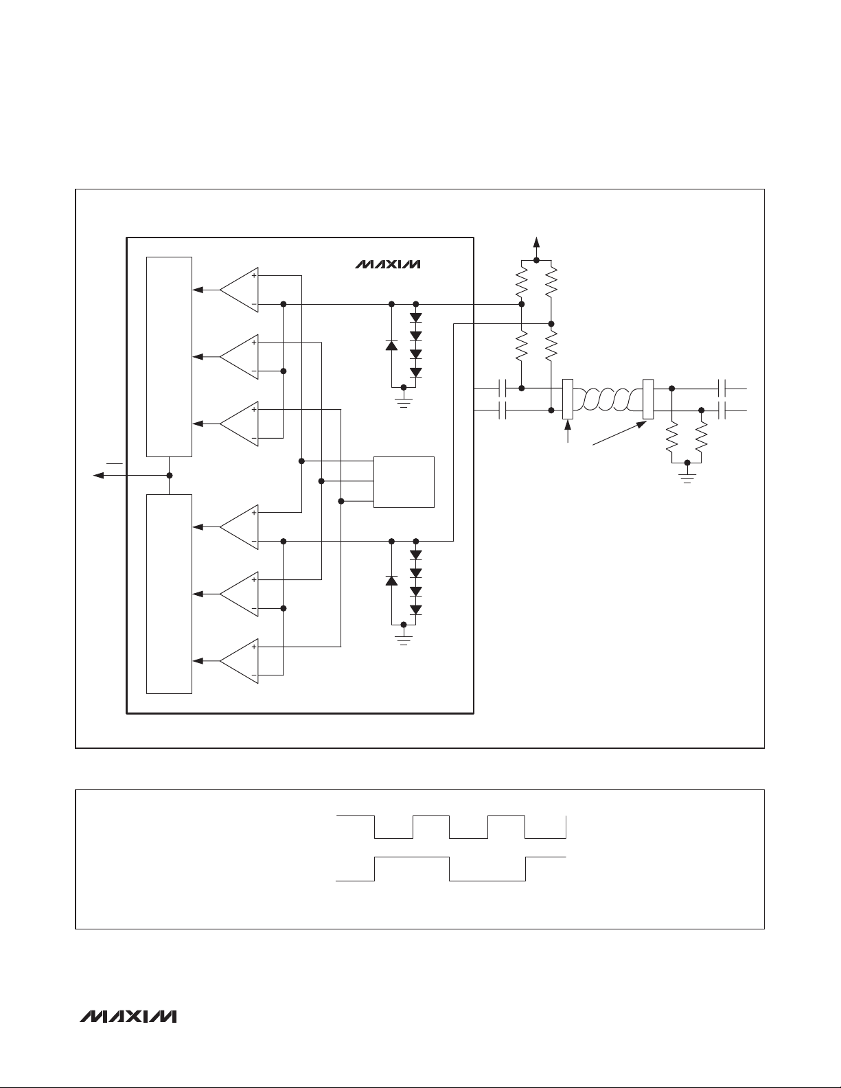
Spectrum and Full-Duplex Control Channel
1.7V TO 1.9V
MAX9259/MAX9260
LFLT
OUTPUT
LOGIC
(OUT+)
OUTPUT
LOGIC
(OUT-)
MAX9259
2.1V
1.5V
0.5V
REFERENCE
VOLTAGE
GENERATOR
45.3kI*
4.99kI*
OUT+
OUT-
LMN0
LMN1
45.3kI*
4.99kI*
TWISTED PAIR
CONNECTORS
*Q1% TOLERANCE
49.9kI*
49.9kI*
Figure 3. Fault-Detector Circuit
NOTE: PCLKIN PROGRAMMED FOR RISING LATCH EDGE.
Figure 4. MAX9259 Worst-Case Pattern Input
______________________________________________________________________________________ 17
PCLKIN
DIN_
Page 18

Gigabit Multimedia Serial Link with Spread
Spectrum and Full-Duplex Control Channel
t
T
t
PCLKIN
HIGH
V
V
IH MIN
IL MAX
t
F
Figure 5. MAX9259 Parallel Input Clock Requirements
t
R
TX/
SCL
MAX9259/MAX9260
t
HOLD
RX/
SDA
P
Figure 6. I2C Timing Parameters
S
t
R
t
F
t
SET
t
LOW
S
P
800mV
t
TSOJ1
2
t
TSOJ1
2
Figure 7. Differential Output Template
18 _____________________________________________________________________________________
Page 19

Gigabit Multimedia Serial Link with Spread
Spectrum and Full-Duplex Control Channel
V
PCLKIN
V
IL MAX
IH MIN
MAX9259/MAX9260
DIN_
Figure 8. MAX9259 Input Setup-and-Hold Times
DIN_
PCLKIN
N
N+1
N+2
t
SET
V
IH MIN
V
IL MAX
NOTE: PCLKIN PROGRAMMED FOR RISING LATCHING EDGE.
EXPANDED TIME SCALE
N+3
N-1
t
HOLD
V
IH MIN
V
IL MAX
N+4
N
OUT+/-
Figure 9. MAX9259 Serializer Delay
______________________________________________________________________________________ 19
t
SD
FIRST BIT LAST BIT
Page 20

Gigabit Multimedia Serial Link with Spread
Spectrum and Full-Duplex Control Channel
PCLKIN
t
LOCK
350Fs
SERIAL LINK INACTIVE SERIAL LINK ACTIVE
REVERSE CONTROL CHANNEL
DISABLED
Figure 10. MAX9259 Link Startup Time
MAX9259/MAX9260
PCLKIN
PWDN
POWERED DOWN
REVERSE CONTROL
CHANNEL DISABLED
V
IH1
Figure 11. MAX9259 Power-Up Delay
PWDN MUST BE HIGH
t
PU
POWERED UP,
SERIAL LINK INACTIVE
REVERSE CONTROL
CHANNEL ENABLED
CHANNEL
DISABLED
REVERSE CONTROL
CHANNEL DISABLED
REVERSE CONTROL CHANNEL
AVAILABLE
POWERED UP, SERIAL LINK ACTIVE
350µs
REVERSE CONTROL
CHANNEL ENABLED
WS
t
SCK
t
LC
t
HC
SCK
t
HOLDtSET
t
HOLDtSET
SD
Figure 12. MAX9259 Input I2S Timing Parameters
20 _____________________________________________________________________________________
Page 21

Gigabit Multimedia Serial Link with Spread
Spectrum and Full-Duplex Control Channel
R
/2
L
V
OD
V
RL/2
CMR
MAX9260
CONTROL-CHANNEL
REVERSE
TRANSMITTER
IN+
IN-
MAX9259/MAX9260
IN+
V
CMR
IN-
V
ROH
0.9 x V
ROH
0.1 x V
(IN+) - (IN-)
ROH
t
R
Figure 13. MAX9260 Reverse Control-Channel Output Parameters
0.1 x V
0.9 x V
ROL
ROL
IN+
IN-
V
ROL
t
F
R
/2
L
RL/2
V
IN+
+
_
C
+
V
IN-
_
IN
V
V
V
ID(P) =
CMR =
ID(P)
IN+
IN-
_
C
IN
| V
- V
|
IN+
IN-
(V
+ V
)/2
IN+
IN-
Figure 14. MAX9260 Test Circuit for Differential Input Measurement
______________________________________________________________________________________ 21
PCLKOUT
DOUT_
NOTE: PCLKOUT PROGRAMMED FOR RISING LATCH EDGE.
Figure 15. MAX9260 Worst-Case Pattern Output
Page 22

Gigabit Multimedia Serial Link with Spread
Spectrum and Full-Duplex Control Channel
t
T
t
PCLKOUT
Figure 16. MAX9260 Clock Output High-and-Low Times
MAX9260
MAX9259/MAX9260
C
L
SINGLE-ENDED OUTPUT LOAD
0.8 x V
I0VCC
t
LOW
HIGH
V
OH MIN
V
OL MAX
Figure 17. MAX9260 Output Rise-and-Fall Times
SERIAL-WORD LENGTH
SERIAL WORD N
IN+/-
FIRST BIT
DOUT_
PCLKOUT
NOTE: PCLKOUT PROGRAMMED FOR RISING LATCHING EDGE.
LAST BIT
PARALLEL WORD N-2
Figure 18. MAX9260 Deserializer Delay
0.2 x V
I0VCC
t
R
SERIAL WORD N+1 SERIAL WORD N+2
PARALLEL WORD N-1 PARALLEL WORD N
t
SD
t
F
22 _____________________________________________________________________________________
Page 23

Gigabit Multimedia Serial Link with Spread
Spectrum and Full-Duplex Control Channel
IN+ - IN-
t
LOCK
MAX9259/MAX9260
Figure 19. MAX9260 Lock Time
Figure 20. MAX9260 Power-Up Delay
LOCK
IN+/-
LOCK
PWDN
PWDN MUST BE HIGH
V
IH1
V
OH
t
PU
V
OH
WS
SCK
SD
Figure 21. MAX9260 Output I2S Timing Parameters
______________________________________________________________________________________ 23
t
t
DVA
DVB
t
DVBtDVA
t
R
t
F
Page 24

Gigabit Multimedia Serial Link with Spread
Spectrum and Full-Duplex Control Channel
Detailed Description
The MAX9259/MAX9260 chipset presents Maxim’s
GMSL technology. The MAX9259 serializer pairs with the
MAX9260 deserializer to form a complete digital serial
link for joint transmission of high-speed video, audio,
and control data for video-display or image-sensing
applications. The serial-payload data rate can reach up
to 2.5Gbps for a 15m STP cable. The parallel interface
is programmable for 24-bit or 32-bit width modes at the
maximum bus clock of 104MHz or 78MHz, respectively.
The minimum bus clock is 6.25MHz for the 32-bit mode
and 8.33MHz for the 24-bit mode. With such a flexible
data configuration, the GMSL is able to support XGA
(1280 x 768) or dual-view WVGA (2 x 854 x 480) display
panels. For image sensing, it supports three 10-bit camera links simultaneously with a pixel clock up to 78MHz.
The 24-bit mode handles 21-bit data and control signals
MAX9259/MAX9260
plus an I2S audio signal. The 32-bit mode handles 29-bit
data and control signals plus an I2S audio signal. Any
combination and sequence of color video data, video
sync, and control signals make up the 21-bit or 29-bit
parallel data on DIN_ and DOUT_. The I2S port supports
the sampled audio data at a rate from 8kHz to 192kHz
and the audio word length of anywhere between 4 to
32 bits. The embedded control channel forms a UART
link between the serializer and deserializer. The UART
link can be set to half-duplex mode or full-duplex mode
depending on the application. The GMSL supports
UART rates from 100kbps to 1Mbps. Using this control
link, a host ECU or FC communicates with the serializer
and deserializer, as well as the peripherals in the remote
side, such as backlight control, grayscale gamma correction, camera module, and touch screen. All serial
communication (forward and reverse) uses differential
signaling. The peripheral programming uses I2C format
or the default GMSL UART format. A separate bypass
mode enables communication using a full-duplex, userdefined UART format. The control link between the
MAX9259 and MAX9260 allows FC connectivity to either
device or peripherals to support video-display or imagesensing applications.
The AC-coupled serial link uses 8B/10B coding. The
MAX9259 serializer features a programmable driver
preemphasis and the MAX9260 deserializer features
a programmable channel equalizer to extend the link
length and enhance the link reliability. Both devices have
a programmable spread-spectrum feature for reducing
EMI on the serial link output (MAX9259) and parallel data
outputs (MAX9260). The differential serial link input and
output pins comply with the ISO 10605 and IEC 610004-2 ESD-protection standards. The core supplies for the
MAX9259/MAX9260 are 1.8V and 3.3V, respectively.
Both devices use an I/O supply from 1.8V to 3.3V
Register Mapping
The FC configures various operating conditions of the
GMSL through registers in the MAX9259/MAX9260.
The default device addresses stored in the R0 and
R1 registers of the MAX9259/MAX9260 are 0x80 and
0x90, respectively. Write to the R0/R1 registers in both
devices to change the device address of the MAX9259
or MAX9260.
Table 1. MAX9259 Power-Up Default Register Map (see Table 18)
REGISTER
ADDRESS
(hex)
0x00 0x80
0x01 0x90
0x02 0x1F, 0x3F
0x03 0x00
24 _____________________________________________________________________________________
POWER-UP DEFAULT
(hex)
POWER-UP DEFAULT SETTINGS
(MSB FIRST)
SERID =1000000, serializer device address is 1000 000
RESERVED = 0
DESID =1001000, deserializer device address is 1001 000
RESERVED = 0
SS = 000 (SSEN = low), SS = 001 (SSEN = high), spread-spectrum settings
depend on SSEN pin state at power-up
AUDIOEN = 1, I2S channel enabled
PRNG = 11, automatically detect the pixel clock range
SRNG = 11, automatically detect serial-data rate
AUTOFM = 00, calibrate spread-modulation rate only once after locking
SDIV = 000000, auto calibrate sawtooth divider
Page 25

Gigabit Multimedia Serial Link with Spread
Spectrum and Full-Duplex Control Channel
Table 1. MAX9259 Power-Up Default Register Map (see Table 18) (continued)
MAX9259/MAX9260
REGISTER
ADDRESS
(hex)
0x04
0x05 0x70
0x06 0x40 RESERVED = 01000000
0x07 0x22 RESERVED = 00100010
0x08
0x0D 0x0F
0x1E
0x1F
POWER-UP DEFAULT
(hex)
0x03, 0x13, 0x83, or
0x93
0x0A
(read only)
0x01
(read only)
0x0X
(read only)
SEREN = 0 (AUTOS = high), SEREN = 1 (AUTOS = low), serial link enable default
depends on AUTOS pin state at power-up
CLINKEN = 0, configuration link disabled
PRBSEN = 0, PRBS test disabled
SLEEP = 0 or 1, sleep mode state depends on CDS and AUTOS pin state at
power-up (see the Link Startup Procedure section)
INTTYPE = 00, base mode uses I2C
REVCCEN = 1, reverse control channel active (receiving)
FWDCCEN = 1, forward control channel active (sending)
I2CMETHOD = 0, I2C packets include register address
DISFPLL = 1, filter PLL disabled
CMLLVL = 11, 400mV CML signal level
PREEMP = 0000, preemphasis disabled
RESERVED = 0000
LFNEG = 10, no faults detected
LFPOS = 10, no faults detected
SETINT = 0, interrupt output set to low
RESERVED = 0001111
ID = 00000001, device ID is 0x01
RESERVED = 0000
REVISION = XXXX, revision number
POWER-UP DEFAULT SETTINGS
(MSB FIRST)
Table 2. MAX9260 Power-Up Default Register Map (see Table 19)
REGISTER
ADDRESS
(hex)
0x00 0x80
0x01 0x90
0x02 0x1F or 0x5F
POWER-UP DEFAULT
(hex)
SERID =1000000, serializer device identifier is 1000 000
RESERVED = 0
DESID =1001000, deserializer device identifier is 1001 000
RESERVED = 0
SS = 00 (SSEN = low), SS = 01 (SSEN = high), spread-spectrum settings depend
on SSEN pin state at power-up
RESERVED = 0
AUDIOEN = 1, I2S channel enabled
PRNG = 11, automatically detect the pixel clock range
SRNG = 11, automatically detect serial-data rate
______________________________________________________________________________________ 25
POWER-UP DEFAULT SETTINGS
(MSB FIRST)
Page 26

Gigabit Multimedia Serial Link with Spread
Spectrum and Full-Duplex Control Channel
Table 2. MAX9260 Power-Up Default Register Map (see Table 19) (continued)
REGISTER
ADDRESS
(hex)
0x03 0x00
0x04
POWER-UP DEFAULT
(hex)
0x03, 0x13, 0x83, or
0x93
AUTOFM = 00, calibrate spread-modulation rate only once after locking
RESERVED = 0
SDIV = 00000, autocalibrate sawtooth divider
LOCKED = 0, LOCK output = low (read only)
OUTENB = 0 (ENABLE = low), OUTENB = 1 (ENABLE = high), OUTENB default
depends on ENABLE pin state at power-up
PRBSEN = 0, PRBS test disabled
SLEEP = 0 or 1, SLEEP setting default depends on CDS and MS pin state at power-up (see the Link Startup Procedure section)
INTTYPE = 00, base mode uses I2C
REVCCEN = 1, reverse control channel active (sending)
FWDCCEN = 1, forward control channel active (receiving)
MAX9259/MAX9260
RESERVED = 0
HPFTUNE = 01, 3.75MHz equalizer highpass cutoff frequency
0x05 0x28 or 0x29
0x06 0x0F
0x07 0x54 RESERVED = 01010100
0x08 0x30 RESERVED = 00110000
0x09 0xC8 RESERVED = 11001000
0x0A 0x12 RESERVED = 00010010
0x0B 0x20 RESERVED = 00100000
0x0C 0x00 ERRTHR = 00000000, error threshold set to zero for decoding errors
0x0D
0x0E
0x12 0x00
0x1E
0x1F
0x00
(read only)
0x00
(read only)
0x02
(read only)
0x0X
(read only)
PDHF = 0, high-frequency boosting disabled
EQTUNE = 1000 (EQS = high, 10.7dB), EQTUNE = 1001 (EQS = low, 5.2dB),
EQTUNE default setting depends on EQS pin state at power-up
DISSTAG = 0, staggered outputs enabled
AUTORST = 0, error registers/output auto reset disabled
DISINT = 0, INT transmission enabled
INT = 0, INT output = low (read only)
GPIO1OUT = 1, GPIO1 output set to high
GPIO1 = 1, GPIO1 input = high (read only)
GPIO0OUT = 1, GPIO0 output set to high
GPIO0 = 1, GPIO0 input = high (read only)
DECERR = 00000000, zero decoding errors detected
PRBSERR = 00000000, zero PRBS errors detected
MCLKSRC = 0, MCLK is derived from PCLKOUT (see Table 5)
MCLKDIV = 0000000, MCLK output is disabled
ID = 00000010, device ID is 0x02
RESERVED = 0000
REVISION = XXXX
POWER-UP DEFAULT SETTINGS
(MSB FIRST)
26 _____________________________________________________________________________________
Page 27

Gigabit Multimedia Serial Link with Spread
Spectrum and Full-Duplex Control Channel
Parallel Inputs and Outputs
The parallel bus uses two selectable bus widths, 24
bits and 32 bits. BWS selects the bus width according
to Table 3. In 24-bit mode, DIN21–DIN28 are not used
and are internally pulled down. For both modes, SD,
SCK, and WS pins are dedicated for I2S audio data. The
assignments of the first 21 or 29 signals are interchangeable and appear in the same order at both sides of the
serial link. In image-sensing applications, disabling the
I2S audio channel (through the MAX9259 and MAX9260
internal registers) allows the MAX9259 to serialize three
10-bit camera data streams through DIN[0:28] plus SD
inputs. The parallel bus accepts data clock rates from
8.33MHz to 104MHz for the 24-bit mode and 6.25MHz to
78MHz for the 32-bit mode.
Serial Link Signaling and Data Format
The MAX9259 high-speed data serial output uses
CML signaling with programmable preemphasis and
AC-coupling. The MAX9260 high-speed receiver uses
AC-coupling and programmable channel equalization.
Together, the GMSL operates at up to 3.125Gbps over
STP cable lengths up to 15m.
The MAX9259 serializer scrambles and encodes the
parallel input bits, and sends the 8B/10B coded sig-
nal through the serial link. The MAX9260 deserializer
MAX9259/MAX9260
recovers the embedded serial clock and then samples,
decodes, and descrambles the data onto the parallel output bus. Figures 22 and 23 show the serial-data
packet format prior to scrambling and 8B/10B coding.
For the 24-bit or 32-bit mode, the first 21 or 29 serial
bits come from DIN[20:0] or DIN[28:0], respectively.
The audio channel bit (ACB) contains an encoded audio
signal derived from the three I2S inputs (SD, SCK, and
WS). The forward control channel (FCC) bit carries the
forward control data. The last bit (PCB) is the parity bit of
the previous 23 or 31 bits.
Reverse Control Channel
The MAX9259/MAX9260 use the reverse control channel
to send I2C/UART and interrupt signals in the opposite
direction of the video stream from the deserializer to
the serializer. The reverse control channel and forward
video data coexist on the same twisted pair forming a
bidirectional link. The reverse control channel operates
independently from the forward control channel. The
reverse control channel is available 500Fs after powerup. The MAX9259 temporarily disables the reverse control channel for 350Fs after starting/stopping the forward
serial link.
Table 3. Bus-Width Selection Using BWS
BWS INPUT STATE BUS WIDTH PARALLEL BUS SIGNALS USED
Low 24 DIN[0:20]/DOUT[0:20], WS, SCK, SD
High 32 DIN[0:28]/DOUT[0:28], WS, SCK, SD
24 BITS
DIN0 DIN1
18-BIT
RGB
DATA
NOTE: LOCATIONS OF THE RGB DATA AND CONTROL SIGNALS ARE
INTERCHANGEABLE ACCORDINGLY ON BOTH SIDES OF THE LINK.
Figure 22. 24-Bit Mode Serial Link Data Format Figure 23. 32-Bit Mode Serial Link Data Format
DIN17 DIN18 DIN19 DIN20 ACB FCC PCB
HSYNC,
VSYNC,
DE
AUDIO
CHANNEL BIT
FORWARD
CONTROL-
CHANNEL BIT
PACKET
PARITY
CHECK BIT
DIN0 DIN1 DIN23 DIN24 DIN25 DIN26 DIN27 DIN28 ACB FCC PCB
24-BIT
RGB DATA
NOTE: LOCATIONS OF THE RGB DATA AND CONTROL SIGNALS ARE
INTERCHANGEABLE ACCORDINGLY ON BOTH SIDES OF THE LINK.
32 BITS
HSYNC,
VSYNC,
DE
ADDITIONAL
VIDEO
DATA/
CONTROL
BITS
AUDIO
CHANNEL
BIT
FORWARD
CONTROLCHANNEL
BIT
PACKET
PARITY
CHECK BIT
______________________________________________________________________________________ 27
Page 28

Gigabit Multimedia Serial Link with Spread
Spectrum and Full-Duplex Control Channel
Table 4. Maximum Audio Sampling Rates for Various PCLK_ Frequencies
PCLK_ FREQUENCY
WORD LENGTH
(Bits)
8
16
18
20
24
32
12.5 15 16.6 > 20 6.25 7.5 8.33 > 10
> 192 > 192 > 192 > 192 > 192 > 192 > 192 > 192
> 192 > 192 > 192 > 192 > 192 > 192 > 192 > 192
185.5 > 192 > 192 > 192 185.5 > 192 > 192 > 192
174.6 > 192 > 192 > 192 174.6 > 192 > 192 > 192
152.2 182.7 > 192 > 192 152.2 182.7 > 192 > 192
123.7 148.4 164.3 > 192 123.7 148.4 164.3 > 192
(DRS = LOW)
(MHz)
Parallel Data-Rate Selection
The MAX9259/MAX9260 use the DRS inputs to set the
MAX9259/MAX9260
parallel data rate. Set DRS high to use a low-speed parallel data rate in the range of 6.25MHz to 12.5MHz (32-bit
mode) or 8.33MHz to 16.66MHz (24-bit mode). Set DRS
low for normal operation with parallel data rates higher
than 12.5MHz (32-bit mode) or 16.66MHz (24-bit mode).
Audio Channel
The I2S audio channel supports audio sampling rates
from 8kHz to 192kHz and audio word lengths from 4 bits
to 32 bits. The audio bit clock (SCK) does not need to be
synchronized with PCLKIN. The MAX9259 automatically
encodes audio data into a single bit stream synchronous
with PCLKIN. The MAX9260 decodes the audio stream
and stores audio words in a FIFO. Audio rate detection
uses an internal oscillator to continuously determine the
audio data rate and output the audio in I2S format. The
audio channel is enabled by default. When the audio
channel is disabled, the SD pins on both sides are
treated as a regular parallel data pin.
PCLK_ frequencies can limit the maximum supported
audio sampling rate. Table 4 lists the maximum audio
sampling rate for various PCLK_ frequencies. Spreadspectrum settings do not affect the I2S data rate or WS
clock frequency.
PCLK_ FREQUENCY
(DRS = HIGH)
(MHz)
Additional MCLK Output
for Audio Applications
Some audio DACs such as the MAX9850 do not require
a synchronous main clock (MCLK), while other DACs
require MCLK to be a specific multiple of WS. If an audio
DAC chip needs the MCLK to be a multiple of WS, synchronize the I2S audio data with PCLK_ of the GMSL,
which is typical for most applications. Select the PCLK_
to be the multiple of WS, or use a clock synthesis chip,
such as the MAX9491, to regenerate the required MCLK
from PCLK_ or SCK.
For audio applications that cannot directly use the
PCLKOUT output, the MAX9260 provides a divided
MCLK output on DOUT28 at the expense of one less
parallel line in 32-bit mode (24-bit mode is not affected).
By default, DOUT28 operates as a parallel data output
and MCLK is turned off. Set MCLKDIV (MAX9260 register 0x12, D[6:0]) to a non-zero value to enable the MCLK
output. Set MCLKDIV to 0x00 to disable MCLK and set
DOUT28 as a parallel data output.
The output MCLK frequency is:
f
f
MCLK
where f
MCLKDIV is the divider ratio from 1 to 127.
is the MCLK source frequency (Table 5) and
SRC
SRC
=
MCLKDIV
28 _____________________________________________________________________________________
Page 29

Gigabit Multimedia Serial Link with Spread
Spectrum and Full-Duplex Control Channel
Table 5. MAX9260 f
MCLKSRC SETTING
(REGISTER 0x12, D7)
0
1
SRC
Settings
DATA-RATE SETTING BIT-WIDTH SETTING
High speed
Low speed
— —
24-bit mode 3 x f
32-bit mode 4 x f
24-bit mode 6 x f
32-bit mode 8 x f
MCLK SOURCE
FREQUENCY (f
PCLKOUT
PCLKOUT
PCLKOUT
PCLKOUT
Internal oscillator
(120MHz typ)
SRC
MAX9259/MAX9260
)
Choose MCLKDIV values so that f
than 60MHz. MCLK frequencies derived from PCLK_
(MCLKSRC = 0) are not affected by spread-spectrum
settings in the deserializer (MAX9260). Enabling spread
spectrum in the serializer (MAX9259), however, introduces spread spectrum into MCLK. Spread-spectrum
settings of either device do not affect MCLK frequencies
derived from the internal oscillator. The internal oscillator frequency ranges from 100MHz to 150MHz over all
process corners and operating conditions.
is not greater
MCLK
Control-Channel and Register Programming
The FC uses the control link to send and receive control
data over the STP link simultaneously with the high-speed
data. Configuring the CDS pin allows the FC to control the
link from either the MAX9259 or the MAX9260 side to support video-display or image-sensing applications.
The control link between the FC and the MAX9259 or
MAX9260 runs in base mode or bypass mode according to the mode selection (MS) input of the device connected to the FC. Base mode is a half-duplex control link
and the bypass mode is a full-duplex control link. In base
mode, the FC is the host and accesses the registers of
both the MAX9259 and MAX9260 from either side of the
link by using the GMSL UART protocol. The FC can also
program the peripherals on the remote side by sending
the UART packets to the MAX9259 or MAX9260, with
UART packets converted to I2C by the device on the
remote side of the link (MAX9260 for LCD or MAX9259
for image-sensing applications). The FC communicates
with a UART peripheral in base mode (through INTTYPE
register settings) using the half-duplex default GMSL
UART protocol of the MAX9259 and MAX9260. The
device addresses of the MAX9259 and MAX9260 in the
base mode are programmable. The default values are
0x80 and 0x90, respectively.
In base mode, when the peripheral interface uses I2C
(default), the MAX9259/MAX9260 only convert packets
that have device addresses different from those of the
MAX9259 or MAX9260 to I2C. The converted I2C bit rate
is the same as the original UART bit rate.
In bypass mode, the FC bypasses the MAX9259/
MAX9260 and communicates with the peripherals directly using its own defined UART protocol. The FC cannot
access the MAX9259/MAX9260’s registers in this mode.
Peripherals accessed through the forward control channel using the UART interface need to handle at least one
PCLK_ period of jitter due to the asynchronous sampling
of the UART signal by PCLK_.
The MAX9259 embeds control signals going to the
MAX9260 in the high-speed forward link. Do not send
a low value longer than 100Fs in either base or bypass
mode. The MAX9260 uses a proprietary differential line
coding to send signals back towards the MAX9259. The
speed of the control link ranges from 100kbps to 1Mbps
in both directions. The MAX9259/MAX9260 automatically
detect the control-channel bit rate in base mode. Packet
bit rates can vary up to 3.5x from the previous bit rate
(see the Changing the Data Frequency section). Figure
24 shows the UART protocol for writing and reading in
base mode between the FC and the MAX9259/MAX9260.
Figure 25 shows the UART data format. Even parity is
used. Figures 26 and 27 detail the formats of the SYNC
byte (0x79) and ACK byte (0xC3). The FC and the connected slave chip generate the SYNC byte and ACK
byte, respectively. Certain events such as device wakeup and interrupt generate signals on the control path and
should be ignored by the FC. All data written to the internal registers do not take affect until after the acknowledge byte is sent. This allows the FC to verify that write
commands are processed without error, even if the result
of the write command directly affects the serial link. The
slave uses the SYNC byte to synchronize with the host
UART data rate automatically. If the INT or MS inputs of
the MAX9260 toggles while there is control-channel communication, the control-channel communication can be
corrupted. In the event of a missed acknowledge, the FC
______________________________________________________________________________________ 29
Page 30

Gigabit Multimedia Serial Link with Spread
Spectrum and Full-Duplex Control Channel
WRITE DATA FORMAT
SYNC DEV ADDR + R/W REG ADDR NUMBER OF BYTES BYTE 1 BYTE N
SYNC DEV ADDR + R/W REG ADDR NUMBER OF BYTES
MASTER WRITES TO SLAVE
Figure 24. UART Protocol for Base Mode
MAX9259/MAX9260
START D0 D1 D2 D3 D4 D5 D6 D7 PARITY STOP
FRAME 1
STOP START STOP START
MASTER WRITES TO SLAVE
READ DATA FRMAT
MASTER READS FROM SLAVE
1 UART FRAME
FRAME 2 FRAME 3
ACK
MASTER READS FROM SLAVE
BYTE NBYTE 1ACK
Figure 25. UART Data Format for Base Mode
D1 D2 D3 D4 D5 D6 D7
STARTD01 0 0 1 1 1 1 0
Figure 26. SYNC Byte (0x79) Figure 27. ACK Byte (0xC3)
PARITY STOP
STARTD01 1 0 0 0 0 1 1
should assume there was an error in the packet when the
D1 D2 D3 D4 D5 D6 D7
Interfacing Command-Byte-Only
slave device receives it, or that an error occurred during
the response from the slave device. In base mode, the
FC must keep the UART Tx/Rx lines high for 16 bit times
before starting to send a new packet.
As shown in Figure 28, the remote-side device converts
the packets going to or coming from the peripherals from
the UART format to the I2C format and vice versa. The
remote device removes the byte number count and adds
or receives the ACK between the data bytes of I2C. The
I2C’s data rate is the same as the UART data rate.
The MAX9259/MAX9260 UART-to-I2C conversion interfaces with devices that do not require register addresses, such as the MAX7324 GPIO expander. Change the
communication method of the I2C master using the
I2CMETHOD bit. I2CMETHOD = 1 sets command-byteonly mode, while I2CMETHOD = 0 sets normal mode
where the first byte in the data stream is the register
address. In this mode, the I2C master ignores the register address byte and directly reads/writes the subsequent data bytes (Figure 29).
30 _____________________________________________________________________________________
PARITY STOP
I2C Devices
Page 31
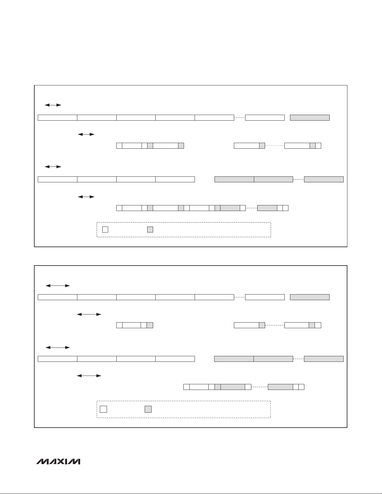
Gigabit Multimedia Serial Link with Spread
Spectrum and Full-Duplex Control Channel
2
C CONVERSION OF WRITE PACKET (I2CMETHOD = 0)
UART-TO-I
FC
MAX9259/MAX9260
11
SYNC FRAME REGISTER ADDRESS NUMBER OF BYTESDEVICE ID + WR DATA 0
11 11 11 11
11 11
DATA N
MAX9259/MAX9260
ACK FRAME
MAX9259/MAX9260 PERIPHERAL
2
C CONVERSION OF READ PACKET (I2CMETHOD = 0)
UART-TO-I
FC
MAX9259/MAX9260 PERIPHERAL
MAX9259/MAX9260
11
SYNC FRAME REGISTER ADDRESS NUMBER OF BYTESDEVICE ID + RD
11 11 11 11
1 11
7
DEV ID A
S
1 17W1
DEV ID AS
: MASTER TO SLAVE
W1REG ADDR8A
REG ADDR8A
: SLAVE TO MASTER
1 1 8 1
ACK FRAME
1 17R1
1
DEV ID AS
S: START P: STOP A: ACKNOWLEDGE
DATA 08A
8
DATA 0 A DATA N A P
11
DATA 0
1
1
DATA N P18A
Figure 28. Format Conversion between UART and I2C with Register Address (I2CMETHOD = 0)
2
UART-TO-I
SYNC FRAME DEVICE ID + WR REGISTER ADDRESS NUMBER OF BYTES DATA 0 DATA N ACK FRAME
MAX9259/MAX9260
C CONVERSION OF WRITE PACKET (I2CMETHOD = 1)
MAX9259/MAX9260FC
11 11 11 11 11 11 11
PERIPHERAL
8 81111 7 1 1
DATA NADATA 0W ADEV IDS A P
11
DATA N
2
UART-TO-I
C CONVERSION OF READ PACKET (I2CMETHOD = 1)
FC
SYNC FRAME
MAX9259/MAX9260
MAX9259/MAX9260
1111 11 11 11 11 11
DEVICE ID + RD REGISTER ADDRESS NUMBER OF BYTES
PERIPHERAL
: MASTER TO SLAVE
: SLAVE TO MASTER S: START P: STOP A: ACKNOWLEDGE
ACK FRAME DATA 0 DATA N
1 1 1 8
S
DEV ID R A A A PDATA 0 DATA N
1 1 17
Figure 29. Format Conversion between UART and I2C in Command-Byte-Only Mode (I2CMETHOD = 1)
______________________________________________________________________________________ 31
8
Page 32

Gigabit Multimedia Serial Link with Spread
Spectrum and Full-Duplex Control Channel
Table 6. MAX9259 CML Driver Strength (Default Level, CMLLVL = 11)
PREEMPHASIS LEVEL
(dB)*
-6.0 0100 12 4 400 200
-4.1 0011 13 3 400 250
-2.5 0010 14 2 400 300
-1.2 0001 15 1 400 350
0 0000 16 0 400 400
1.1 1000 16 1 425 375
2.2 1001 16 2 450 350
3.3 1010 16 3 475 325
4.4 1011 16 4 500 300
6.0 1100 15 5 500 250
MAX9259/MAX9260
*Negative preemphasis levels denote deemphasis.
8.0 1101 14 6 500 200
10.5 1110 13 7 500 150
14.0 1111 12 8 500 100
PREEMPHASIS SETTING
(0x05, D[3:0])
I
CML
(mA)
I
PRE
(mA)
SINGLE-ENDED VOLTAGE SWING
MAX
(mV)
MIN
(mV)
Interrupt Control
The INT of the MAX9259 is the interrupt output and the
INT of the MAX9260 is the interrupt input. The interrupt
output on the MAX9259 follows the transitions at the
interrupt input of the MAX9260. This interrupt function
supports remote-side functions such as touch-screen
peripherals, remote power-up, or remote monitoring.
Interrupts that occur during periods where the reverse
control channel is disabled, such as link startup/shutdown, are automatically resent once the reverse control
channel becomes available again. Bit D4 of register
0x06 in the MAX9260 also stores the interrupt input state.
Writing to the SETINT register bit also sets the INT output
of the MAX9259. In addition, the FC sets the INT output
of the MAX9259 by writing to the SETINT register bit. In
normal operation, the state of the interrupt output changes when the interrupt input on the MAX9260 toggles.
Preemphasis Driver
The serial line driver in the MAX9259 employs currentmode logic (CML) signaling. The driver generates
an adjustable preemphasized waveform according to
the cable length and characteristics. There are 13
preemphasis settings, as shown in Table 6. Negative
preemphasis levels are deemphasis levels in which the
preemphasized swing level is the same as normal swing,
but the no-transition data is deemphasized. Program the
preemphasis levels through register 0x05 D[3:0] of the
MAX9259. This preemphasis function compensates the
high-frequency loss of the cable and enables reliable
transmission over longer link distances. Additionally, a
lower power drive mode can be entered by programming CMLLVL bits (0x05 D[5:4]) to reduce the driver
strength down to 75% (CMLLVL = 10), or 50% (CMLLVL
= 01) from 100% (CMLLVL = 11, default).
Line Equalizer
The MAX9260 includes an adjustable line equalizer to
further compensate cable attenuation at high frequencies. The cable equalizer has 11 selectable levels of
compensation from 2.1dB to 13dB (Table 7). The EQS
input selects the default equalization level at power-up.
The state of EQS is latched upon power-up or when
resuming from power-down mode. To select other
equalization levels, set the corresponding register bits
in the MAX9260 (0x05 D[3:0]). Use equalization in the
MAX9260, together with preemphasis in the MAX9259 to
create the most reliable link for a given cable.
32 _____________________________________________________________________________________
Page 33

Gigabit Multimedia Serial Link with Spread
Spectrum and Full-Duplex Control Channel
Table 7. MAX9260 Cable Equalizer Boost
Levels
BOOST SETTING
(0x05 D[3:0])
0000 2.1
0001 2.8
0010 3.4
0011 4.2
0100
0101 6.2
0110 7
0111 8.2
1000 9.4
1001
1010 11.7
1011 13
TYPICAL BOOST GAIN (dB)
5.2
Power-up default
(EQS = high)
10.7
Power-up default
(EQS = low)
Spread Spectrum
MAX9259/MAX9260
To reduce the EMI generated by the transitions on the
serial link and parallel outputs, both the MAX9259 and
MAX9260 support spread spectrum. Turning on spread
spectrum on the MAX9260 spreads the parallel video
outputs. Turning on spread spectrum on the MAX9259
spreads the serial link, along with the MAX9260 parallel
outputs. Do not enable spread spectrum for both the
MAX9259 and MAX9260. The six selectable spreadspectrum rates at the MAX9259 serial output are Q0.5%,
Q1%, Q1.5%, Q2%, Q3%, and Q4% (Table 8). Some
spread-spectrum rates can only be used at lower PCLK_
frequencies (Table 9). There is no PCLK_ frequency limit
for the 0.5% spread rate. The two selectable spreadspectrum rates at the MAX9260 parallel outputs are Q2%
and Q4% (Table 10).
Set the MAX9259 SSEN input high to select 0.5% spread
at power-up and SSEN input low to select no spread at
power-up. Set the MAX9260 SSEN input high to select
2% spread at power-up and SSEN input low to select no
spread at power-up. The state of SSEN is latched upon
power-up or when resuming from power-down mode.
Whenever the MAX9259 spread spectrum is turned on
Table 8. MAX9259 Serial Output Spread
SS SPREAD (%)
000 No spread spectrum. Power-up default when SSEN = low.
001
010
011
100 No spread spectrum
101
110
111
Q0.5% spread spectrum. Power-up default when SSEN = high.
Q1.5% spread spectrum
Q2% spread spectrum
Q1% spread spectrum
Q3% spread spectrum
Q4% spread spectrum
Table 9. MAX9259 Spread-Spectrum Rate Limitations
24-BIT MODE PCLKIN
FREQUENCY
(MHz)
< 33.3 < 25 < 1000 All rates available
33.3 to < 66.7 20 to < 50 1000 to < 2000 1.5%, 1.0%, 0.5%
66.7+ 50+ 2000+ 0.5%
32-BIT MODE PCLKIN
FREQUENCY
(MHz)
SERIAL LINK BIT RATE
(Mbps)
AVAILABLE SPREAD RATES
______________________________________________________________________________________ 33
Page 34

Gigabit Multimedia Serial Link with Spread
Spectrum and Full-Duplex Control Channel
Table 10. MAX9260 Parallel Output Spread
SS SPREAD (%)
00 No spread spectrum. Power-up default when SSEN = low.
01
10 No spread spectrum
11
Table 11. MAX9259 Modulation Coefficients and Maximum SDIV Settings
BIT-WIDTH MODE
32-Bit
MAX9259/MAX9260
24-Bit
Q2% spread spectrum. Power-up default when SSEN = high.
Q4% spread spectrum
SPREAD-SPECTRUM
SETTING (%)
1 104 40
0.5 104 63
3 152 27
1.5 152 54
4 204 15
2 204 30
1 80 52
0.5 80 63
3 112 37
1.5 112 63
4 152 21
2 152 42
MODULATION
COEFFICIENT (decimal)
SDIV UPPER LIMIT (deci-
mal)
Table 12. MAX9260 Modulation Coefficients and Maximum SDIV Settings
SPREAD-SPECTRUM SETTING (%)
4 208 15
2 208 30
or off, the serial link automatically restarts and remains
unavailable while the MAX9260 relocks to the serial data.
Turning on spread spectrum on either the MAX9259 or
MAX9260 side does not affect the audio data stream.
Changes in the MAX9259 spread settings only affect
MCLK output if it is derived from PCLK_ (MCLKSRC = 0).
Both devices include a sawtooth divider to control the
spread-modulation rate. Autodetection or manual programming of the PCLK_ operation range guarantees a
spread-spectrum modulation frequency within 20kHz to
40kHz. Additionally, manual configuration of the sawtooth divider (SDIV, 0x03 D[5:0]) allows the user to set a
specific modulation frequency for a specific PCLK_ rate.
Always keep the modulation frequency between 20kHz
to 40kHz to ensure proper operation.
34 _____________________________________________________________________________________
MODULATION COEFFICIENT (deci-
mal)
Manual Programming of the Spread-
The modulation rates for the MAX9259 or the MAX9260
relate to the PCLK_ frequency as follows:
where:
fM = Modulation frequency
DRS = DRS pin input value (0 or 1)
f
= Parallel clock frequency (12.5MHz to 104MHz)
PCLK_
MOD = Modulation coefficient given in Table 11 for the
MAX9259 and Table 12 for the MAX9260
SDIV = 6-bit (MAX9259) or 5-bit (MAX9260) SDIV setting,
manually programmed by the FC
SDIV UPPER LIMIT (decimal)
f 1 DRS
= +
( )
M
Spectrum Divider
f
PCLK_
MOD SDIV
×
Page 35

Gigabit Multimedia Serial Link with Spread
Spectrum and Full-Duplex Control Channel
To program the SDIV setting, first look up the modulation
coefficient according to the part number and desired
bit-width and spread-spectrum settings. Solve the above
equation for SDIV using the desired parallel clock and
modulation frequencies. If the calculated SDIV value is
larger than the maximum allowed SDIV value in Tables
11 or 12, set SDIV to the maximum value.
Sleep Mode
The serializer/deserializer include a low-power sleep
mode to reduce power consumption on the device not
attached to the FC (MAX9260 in LCD applications and
MAX9259 in camera applications). Set the corresponding remote IC’s SLEEP bit to 1 to initiate sleep mode. The
MAX9259 sleeps immediately after setting its SLEEP =
1. The MAX9260 sleeps after serial link inactivity or 8ms
(whichever arrives first) after setting its SLEEP = 1. See
the Link Startup Procedure section for details on waking
up the device for different FC and starting conditions.
The FC side device cannot enter into sleep mode, and its
SLEEP bit remains at 0. Use the PWDN input pin to bring
the FC side device into a low-power state.
Configuration Link Mode
The MAX9259/MAX9260 include a low-speed configuration link to allow control-data connection between the two
devices in the absence of a valid parallel clock input. In
either display or camera applications, the configuration
link can be used to program equalizer/preemphasis
or other registers before establishing the video link.
An internal oscillator provides PCLK_ for establishing
the serial configuration link between the MAX9259 and
MAX9260. The parallel output clock and data lines are
disabled in the MAX9260. The LOCK output remains
low even after a successful configuration link lock. Set
CLINKEN = 1 on the MAX9259 to turn on the configuration link. The configuration link remains active as long as
the video link has not been enabled. The video link overrides the configuration link and attempts to lock when
SEREN = 1.
Link Startup Procedure
Table 13 lists four startup cases for video-display
applications. Table 14 lists two startup cases for imagesensing applications. In either display or image-sensing
applications, the control link is always available after
the high-speed data link or the configuration link is
established and the MAX9259/MAX9260 registers or the
peripherals are ready for programming.
Video-Display Applications
MAX9259/MAX9260
For the video-display application, with a remote display
unit, connect the FC to the serializer (MAX9259) and set
CDS = low for both the MAX9259 and MAX9260. Table
13 summarizes the four startup cases based on the settings of AUTOS and MS.
Case 1: Autostart Mode
After power-up or when PWDN transitions from low
to high for both the serializer and deserializer, the
serial link establishes if a stable PCLK_ is present. The
MAX9259 locks to PCLK_ and sends the serial data to
the MAX9260. The MAX9260 then detects activity on the
serial link and locks to the input serial data.
Case 2: Standby Start Mode
After power-up, or when PWDN transitions from low
to high for both the serializer and deserializer, the
MAX9260 starts up in sleep mode, and the MAX9259
stays in standby mode (does not send serial data). Use
the FC and program the MAX9259 to set SEREN = 1 to
establish a video link or CLINKEN = 1 to establish the
configuration link. After locking to a stable PCLK_ (for
SEREN = 1) or the internal oscillator (for CLINKEN = 1),
the MAX9259 sends a wake-up signal to the deserializer. The MAX9260 exits sleep mode after locking to the
serial data and sets SLEEP = 0. If after 8ms the deserializer does not lock to the input serial data, the MAX9260
goes back to sleep, and the internal sleep bit remains
uncleared (SLEEP = 1).
Case 3: Remote Side Autostart Mode
After power-up, or when PWDN transitions from low to
high, the remote device (MAX9260) starts up and tries
to lock to an incoming serial signal with sufficient power.
The host side (MAX9259) is in standby mode and does
not try to establish a link. Use the FC and program the
MAX9259 to set SEREN = 1 (and apply a stable PCLK_)
to establish a video link, or CLINKEN = 1 to establish the
configuration link. In this case, the MAX9260 ignores the
short wake-up signal sent from the MAX9259.
Case 4: Remote Side in Sleep Mode
After power-up or when PWDN transitions from low to
high, the remote device (MAX9260) starts up in sleep
mode. The high-speed link establishes automatically
after MAX9259 powers up with a stable PCLK_ and
sends a wake-up signal to the MAX9260. Use this mode
in applications where the MAX9260 powers up before
the MAX9259.
______________________________________________________________________________________ 35
Page 36

Gigabit Multimedia Serial Link with Spread
Spectrum and Full-Duplex Control Channel
Table 13. Startup Selection for Video-Display Applications (CDS = Low)
CASE
AUTOS
(MAX9259)
MAX9259
POWER-UP STATEMS(MAX9260)
1 Low Serialization enabled Low
2 High
3 High
Serialization dis-
abled
Serialization dis-
abled
MAX9259/MAX9260
4 Low Serialization enabled High
High
Low
MAX9260
POWER-UP STATE
Normal
(SLEEP = 0)
Sleep mode
(SLEEP = 1)
Normal
(SLEEP = 0)
Sleep mode
(SLEEP = 1)
LINK STARTUP MODE
Both devices power up with
serial link active (autostart)
Serial link is disabled and
the MAX9260 powers up in
sleep mode. Set SEREN = 1 or
CLINKEN = 1 in the MAX9259
to start the serial link and wake
up the MAX9260.
Both devices power up in normal mode with the serial link
is disabled. Set SEREN = 1 or
CLINKEN = 1 in the MAX9259
to start the serial link.
MAX9260 starts in sleep mode.
Link autostarts upon MAX9259
power-up. Use this case when
the MAX9260 powers up before
the MAX9259.
AUTOS PIN
SETTING
LOW
HIGH
SEREN BIT
POWER-UP VALUE
PWDN = LOW OR
POWER-OFF
ALL STATES
1
0
POWER-DOWN
OR POWER-OFF
PWDN = HIGH
POWER-ON,
AUTOS = LOW
PWDN = HIGH,
POWER-ON
AUTOS = LOW
SEREN = 1,
PCLKIN RUNNING
VIDEO
LINK LOCKING
POWER-ON
IDLE
SEREN = 0, OR
NO PCLKIN
VIDEO LINK
LOCKED
VIDEO LINK
UNLOCKED
Figure 30. MAX9259 State Diagram, CDS = Low (LCD Application)
CLINKEN = 0 OR
SEREN = 1
CLINKEN = 1
SEREN = 0,
NO PCLKIN
VIDEO LINK
OPERATING
CLINKEN = 0 OR
SEREN = 1
CONFIG
LINK STARTING
PRBSEN = 0
PRBSEN = 1
CONFIG LINK
UNLOCKED
CONFIG LINK
LOCKED
VIDEO LINK
PRBS TEST
CONFIG LINK
OPERATING
PROGRAM
REGISTERS
36 _____________________________________________________________________________________
Page 37

Gigabit Multimedia Serial Link with Spread
Spectrum and Full-Duplex Control Channel
SLEEP = 1, VIDEO LINK OR CONFIG
LINK NOT LOCKED AFTER 8ms
MAX9259/MAX9260
MS PIN
SETTING
LOW
HIGH
SEND INT TO
MAX9259
SLEEP BIT
POWER-UP VALUE
0
1
SERIAL LINK ACTIVITY STOPS OR 8ms ELAPSES AFTER
INT CHANGES FROM
LOW TO HIGH OR
HIGH TO LOW
SLEEP
FC SETS SLEEP = 1
ALL STATES
WAKE-UP
SIGNAL
PWDN = LOW OR
POWER-OFF
POWER-ON
IDLE
POWER-DOWN
POWER-OFF
Figure 31. MAX9260 State Diagram, CDS = Low (LCD Application)
Image-Sensing Applications
For image-sensing applications, with remote camera
unit(s), connect the FC to the deserializer (MAX9260)
and set CDS = high for both the MAX9259 and MAX9260.
The MAX9260 powers up normally (SLEEP = 0) and continuously tries to lock to a valid serial input. Table 14
summarizes the two startup cases, based on the state of
the MAX9259 AUTOS pin.
Case 1: Autostart Mode
After power-up, or when PWDN transitions from low to
high, the MAX9259 locks to a stable PCLKIN and sends
the high-speed data to the MAX9260. The MAX9260
locks to the serial data and outputs the parallel video
data and PCLKOUT.
SIGNAL
DETECTED
PWDN = HIGH,
POWER-ON
OR
SERIAL PORT
VIDEO LINK
LOCKED
VIDEO LINK
OPERATING
LOCKING
0 SLEEP
CONFIG LINK
UNLOCKED
CONFIG LINK
LOCKED
PRBSEN = 0
PRBSEN = 1
VIDEO LINK
UNLOCKED
VIDEO LINK
PRBS TEST
CONFIG LINK
OPERATING
PROGRAM
REGISTERS
0 SLEEP
Case 2: Sleep Mode
After power-up, or when PWDN transitions from low to
high, the MAX9259 starts up in sleep mode. To wake up
the MAX9259, use the FC to send a regular UART frame
containing at least three rising edges (e.g., 0x66), at a
bit rate no greater than 1Mbps. The low-power wake-up
receiver of the MAX9259 detects the wake-up frame over
the reverse control channel and powers up. Reset the
sleep bit (SLEEP = 0) of the MAX9259 using a regular
control-channel write packet to power up the device fully.
Send the sleep bit write packet at least 500Fs after the
wake-up frame. The MAX9259 goes back to sleep mode
if its sleep bit is not cleared within 8ms (typ) after detecting a wake-up frame.
Table 14. Startup Selection for Image-Sensing Applications (CDS = High)
CASE
AUTOS
(MAX9259)
MAX9259 POWER-UP
STATE
1 Low Serialization enabled
2 High
Sleep mode
(SLEEP = 1)
______________________________________________________________________________________ 37
MAX9260 POWER-UP
STATE
Normal
(SLEEP = 0)
Normal
(SLEEP = 0)
LINK STARTUP MODE
Autostart
MAX9259 is in sleep mode. Wake
up the MAX9259 through the control
channel (FC attached to MAX9260).
Page 38

Gigabit Multimedia Serial Link with Spread
Spectrum and Full-Duplex Control Channel
POWER-UP VALUE
SEREN SLEEP
1
0
SLEEP = 1
FOR > 8ms
REVERSE LINK
WAKE-UP SIGNAL
PWDN = HIGH,
POWER-ON,
AUTOS = HIGH
POWER-DOWN
POWER-OFF
0
1
OR
WAKE-UP
SLEEP = 0,
SLEEP = 1
PWDN = HIGH,
POWER-ON
AUTOS = LOW
SLEEP = 0,
SEREN = 0
SEREN = 1,
PCLKIN RUNNING
VIDEO
LINK LOCKING
SLEEP = 1
ALL STATES
AUTOS PIN
SETTING
LOW
HIGH
SLEEP
PWDN = LOW OR
POWER-OFF
MAX9259/MAX9260
Figure 32. MAX9259 State Diagram, CDS = High (Camera Application)
POWER-ON
IDLE
(REVERSE
CHANNEL
ACTIVE)
SIGNAL
DETECTED
SEREN = 0 OR
NO PCLKIN
VIDEO LINK
LOCKED
VIDEO LINK
UNLOCKED
SERIAL PORT
LOCKING
POWER-ON
IDLE
CLINKEN = 0 OR
CLINKEN = 1
CONFIG LINK
UNLOCKED
CONFIG LINK
LOCKED
SEREN = 1
SEREN = 0 OR
NO PCLKIN
VIDEO LINK
OPERATING
CLINKEN = 0 OR
SEREN = 1
CONFIG
LINK STARTED
PRBSEN = 0
PRBSEN = 1
CONFIG
LINK OPERATING
PROGRAM
REGISTERS
CONFIG LINK
UNLOCKED
CONFIG LINK
LOCKED
VIDEO LINK
PRBS TEST
CONFIG LINK
OPERATING
PROGRAM
REGISTERS
NO SIGNAL
DETECTED
ALL STATES
PWDN = LOW OR
POWER-OFF
PWDN = HIGH,
POWER ON
POWER-DOWN
OR
POWER-OFF
VIDEO LINK
LOCKED
VIDEO LINK
UNLOCKED
VIDEO LINK
OPERATING
PRBSEN = 0
PRBSEN = 1
VIDEO LINK
PRBS TEST
Figure 33. MAX9260 State Diagram, CDS = High (Camera Application)
38 _____________________________________________________________________________________
Page 39

Gigabit Multimedia Serial Link with Spread
Spectrum and Full-Duplex Control Channel
Applications Information
MAX9260 Error Checking
The MAX9260 checks the serial link for errors and stores
the number of detected decoding errors in the 8-bit
register (DECERR, 0x0D). If a large number of decoding
errors are detected within a short duration, the deserializer loses lock and stops the error counter. The deserializer then attempts to relock to the serial data. DECERR
resets upon successful video link lock, successful
readout of DECERR (through UART), or whenever autoerror reset is enabled. The MAX9260 does not check
for decoding errors during the internal PRBS test and
DECERR is reset to 0x00.
ERR Output
The MAX9260 has an open-drain ERR output. This
output asserts low whenever the number of decoding
errors exceed the error threshold (ERRTHR, 0x0C) during normal operation, or when at least one PRBS error is
detected during PRBS test. ERR reasserts high whenever DECERR (0x0D) resets, due to DECERR readout,
video link lock, or autoerror reset.
Autoerror Reset
The default method to reset errors is to read the respective error registers in the MAX9260 (0x0D, 0x0E). Autoerror reset clears the decoding-error counter (DECERR)
and the ERR output ~1Fs after ERR goes low. Autoerror
reset is disabled on power-up. Enable autoerror reset
through AUTORST (0x06 D6). Autoerror reset does not
run when the device is in PRBS test mode.
Self PRBS Test
The MAX9259/MAX9260 link includes a PRBS pattern generator and bit-error verification function. Set
PRBSEN = 1 (0x04 D5) first in the MAX9259 and then
the MAX9260 to start the PRBS test. Set PRBSEN = 0
(0x04 D5) first in the MAX9260 and then the MAX9259
to exit the PRBS self test. The MAX9260 uses an 8-bit
register (0x0E) to count the number of detected errors.
The control link also controls the start and stop of the
error counting. During PRBS mode, the device does not
count decoding errors and the ERR output reflects PRBS
errors only. Autoerror reset does not run when the device
is in PRBS mode.
Microcontrollers on Both Sides
of the GMSL Link (Dual µC Control)
Usually the FC is either on the serializer (MAX9259)
side for video-display applications, or on the deserializer (MAX9260) side for image-sensing applications. For
the former case, both the CDS pins of the MAX9259/
MAX9260 are set to low, and for the later case, the
CDS pins are set to high. However, if the CDS pin of the
MAX9259 is low and the CDS pin of the MAX9260 is high,
then the MAX9259/MAX9260 can both connect to FCs
simultaneously. In such a case, the FCs on either side
can communicate with the MAX9259/MAX9260 UART
protocol.
Contentions of the control link may happen if the FCs
on both sides are using the link at the same time. The
MAX9259/MAX9260 do not provide the solution for
contention avoidance. The serializer/deserealizer do not
send an acknowledge frame when communication fails
due to contention. Users can always implement a higherlayer protocol to avoid the contention. In addition, if UART
communication across the serial link is not required, the
FCs can disable the forward and reverse control channel
through the FWDCCEN and REVCCEN bits (0x04 D[1:0])
in the MAX9259/MAX9260. UART communication across
the serial link is stopped and contention between FCs no
longer occurs. During the dual FC operation, if one of the
CDS pins on either side changes state, the link resumes
the corresponding state described in the Link Startup
Procedure section.
As an example of dual FC use in an image-sensing link,
the MAX9259 may be in sleep mode and waiting to be
waked up by the MAX9260. After wake-up, the serializerside FC sets the MAX9259 CDS pin low and assumes
master control of the MAX9259 registers.
Jitter-Filtering PLL
In some applications, the parallel bus input clock to the
MAX9259 (PCLKIN) includes noise, which reduces link
reliability. The MAX9259 has a narrow-band jitter-filtering
PLL to attenuate frequency components outside the
PLL’s bandwidth (< 100kHz typ). Enable the jitter-filtering
PLL by setting DISFPLL = 0 (0x05 D6).
Changing the Data Frequency
Both the video data rate (f
rate (f
applications with multiple clock speeds. Slow speed/
performance modes allow significant power savings
when a system’s full capabilities are not required. Enable
the MAX9259/MAX9260 link after PCLK_ stabilizes.
Stop PCLKIN for 5µs and restart the serial link or toggle
SEREN after each change in the parallel clock frequency
to recalibrate any automatic settings if a clean frequency
change cannot be guaranteed. The reverse control
channel remains unavailable for 350Fs after serial link
start or stop. Limit on-the-fly changes in f
tors of less than 3.5 at a time to ensure that the device
) can be changed on-the-fly to support
UART
) and the control data
PCLK_
UART
to fac-
MAX9259/MAX9260
______________________________________________________________________________________ 39
Page 40

Gigabit Multimedia Serial Link with Spread
Spectrum and Full-Duplex Control Channel
recognizes the UART sync pattern. For example, when
lowering the UART frequency from 1Mbps to 100kbps,
first send data at 333kbps and then at 100kbps to have
reduction ratios of 3 and 3.333, respectively.
LOCK Output Loopback
Connect the LOCK output to the INT input of the
MAX9260 to loopback LOCK to the MAX9259. The
interrupt output on the MAX9259 follows the transitions
at the LOCK output of the MAX9260. Reverse-channel
communication does not require an active forward link
to operate and accurately tracks the LOCK status of the
video link. LOCK asserts for video link only and not for
the configuration link.
MAX9260 GPIOs
The MAX9260 has two open-drain GPIOs available.
GPIO1OUT and GPIO0OUT (0x06 D3, D1) set the output
MAX9259/MAX9260
state of the GPIOs. The GPIO input buffers are always
enabled. The input states are stored in GPIO1 and
GPIO0 (0x06 D2, D0). Set GPIO1OUT/GPIO0OUT to 1
when using GPIO1/GPIO0 as an input.
Line-Fault Detection
The line-fault detector in the MAX9259 monitors for line
failures such as short to ground, short to power supply,
and open link for system fault diagnosis. Figure 3 shows
the required external resistor connections. LFLT = low
when a line fault is detected and LFLT = high when the
line returns to normal. The line-fault type is stored in
0x08 D[3:0] of the MAX9259. The fault-detector threshold voltages are referenced to the MAX9259 ground.
Additional passive components set the DC level of the
cable (Figure 3). If the MAX9259 and MAX9260 grounds
are different, the link DC voltage during normal operation
can vary and cross one of the fault-detection thresholds.
For the fault-detection circuit, select the resistor’s power
rating to handle a short to the battery. Table 15 lists the
mapping for line-fault types.
Staggered Parallel Data Outputs
The MAX9260 staggers the parallel data outputs to
reduce EMI and noise. Staggering outputs also reduce
the power-supply transient requirements. By default,
the deserializer staggers outputs according to Table
16. Disable output staggering through the DISSTAG bit
(0x06 D7)
Choosing I2C/UART Pullup Resistors
Both I2C/UART open-drain lines require pullup resistors
to provide a logic-high level. There are tradeoffs between
power dissipation and speed, and a compromise must
be made in choosing pullup resistor values. Every device
connected to the bus introduces some capacitance even
when the device is not in operation. I2C specifies 300ns
rise times to go from low to high (30% to 70%) for fast
mode, which is defined for data rates up to 400kbps (see
the I2C specifications in the Electrical Characteristics
table for details). To meet the fast-mode rise-time
requirement, choose the pullup resistors so that rise time
tR = 0.85 x R
are not recognized if the transition time becomes too
PULLUP
x C
< 300ns. The waveforms
BUS
Table 16. Staggered Output Delay
OUTPUT DELAY RELATIVE
OUTPUT
DISSTAG = 0 DISSTAG = 1
DOUT0–DOUT5,
DOUT21, DOUT22
DOUT6–DOUT10,
DOUT23, DOUT24
DOUT11–DOUT15,
DOUT25, DOUT26
DOUT16–DOUT20,
DOUT27, DOUT28
PCLKOUT 0.75 0
TO DOUT0 (ns)
0 0
0.5 0
1 0
1.5 0
Table 15. MAX9259 Line-Fault Mapping
REGISTER
ADDRESS
0x08
40 _____________________________________________________________________________________
BITS NAME VALUE LINE-FAULT TYPE
00 Negative cable wire shorted to battery
D[3:2] LFNEG
D[1:0] LFPOS
01 Negative cable wire shorted to ground
10 Normal operation
11 Negative cable wire open
00 Positive cable wire shorted to battery
01 Positive cable wire shorted to ground
10 Normal operation
11 Positive cable wire open
Page 41

Gigabit Multimedia Serial Link with Spread
Spectrum and Full-Duplex Control Channel
slow. The MAX9259/MAX9260 support I2C/UART rates
up to 1Mbps.
AC-Coupling
AC-coupling isolates the receiver from DC voltages up to
the voltage rating of the capacitor. Four capacitors—two
at the serializer output and two at the deserializer input—
are needed for proper link operation and to provide
protection if either end of the cable is shorted to a high
voltage. AC-coupling blocks low-frequency ground shifts
and low-frequency common-mode noise.
Selection of AC-Coupling Capacitors
Voltage droop and the digital sum variation (DSV) of
transmitted symbols cause signal transitions to start
from different voltage levels. Because the transition time
is finite, starting the signal transition from different voltage levels causes timing jitter. The time constant for an
AC-coupled link needs to be chosen to reduce droop
and jitter to an acceptable level. The RC network for an
AC-coupled link consists of the CML receiver termination
resistor (RTR), the CML driver termination resistor (RTD),
and the series AC-coupling capacitors (C). The RC time
constant for four equal-value series capacitors is (C x
(RTD + RTR))/4. RTD and RTR are required to match the
transmission line impedance (usually 100I). This leaves
the capacitor selection to change the system time constant. Use at least 0.2FF (100V) high-frequency surfacemount ceramic capacitors to pass the lower speed
reverse-channel signal. Use capacitors with a case size
less than 3.2mm x 1.6mm to have lower parasitic effects
to the high-speed signal.
Power-Supply Circuits and Bypassing
The MAX9259 uses an AVDD and DVDD of 1.7V to 1.9V.
The MAX9260 uses an AVDD and DVDD of 3.0V to 3.6V.
All single-ended inputs and outputs on the MAX9259/
MAX9260 derive power from an IOVDD of 1.7V to 3.6V.
MAX9259/MAX9260
The input levels or output levels scale with IOVDD.
Proper voltage-supply bypassing is essential for highfrequency circuit stability.
Cables and Connectors
Interconnect for CML typically has a differential impedance of 100I. Use cables and connectors that have
matched differential impedance to minimize impedance
discontinuities. Twisted-pair and shielded twisted-pair
cables offer superior signal quality compared to ribbon
cable and tend to generate less EMI due to magneticfield canceling effects. Balanced cables pick up noise
as common mode rejected by the CML receiver. Table
17 lists the suggested cables and connectors used in
the GMSL link.
Board Layout
Separate the parallel signals and CML high-speed serial
signals to prevent crosstalk. Use a four-layer PCB with
separate layers for power, ground, CML, and digital
signals. Layout PCB traces close to each other and have
a 100I differential characteristic impedance. The trace
dimensions depend on the type of trace used (microstrip
or stripline). Note that two 50I PCB traces do not
have 100I differential impedance when brought close
together—the impedance goes down when the traces
are brought closer.
Route the PCB traces for a CML channel (there are two
conductors per CML channel) in parallel to maintain the
differential characteristic impedance. Avoid vias. If vias
must be used, use only one pair per CML channel and
place the via for each line at the same point along the
length of the PCB traces. This way, any reflections occur
at the same time. Do not make vias into test points for
Table 17. Suggested Connectors and Cables for GMSL
SUPPLIER CONNECTOR CABLE
JAE Electronics, Inc. MX38-FF A-BW-Lxxxxx
Nissei Electric Co., Ltd. GT11L-2S F-2WME AWG28
Rosenberger Hochfrequenztechnik GmbH D4S10A-40ML5-Z Dacar 538
______________________________________________________________________________________ 41
Page 42

Gigabit Multimedia Serial Link with Spread
Spectrum and Full-Duplex Control Channel
R
D
1.5kI
DISCHARGE
RESISTANCE
STORAGE
CAPACITOR
DEVICE
UNDER
HIGH-
VOLTAGE
DC
SOURCE
1MI
CHARGE-CURRENT-
LIMIT RESISTOR
C
S
100pF
Figure 34. Human Body Model ESD Test Circuit
R
D
330I
HIGH-
VOLTAGE
DC
SOURCE
CHARGE-CURRENT-
LIMIT RESISTOR
150pF
MAX9259/MAX9260
C
S
DISCHARGE
RESISTANCE
STORAGE
CAPACITOR
DEVICE
UNDER
Figure 35. IEC 61000-4-2 Contact Discharge ESD Test Circuit
TEST
TEST
ATE. Keep PCB traces that make up a differential pair
equal in length to avoid skew within the differential pair.
ESD Protection
The MAX9259/MAX9260 ESD tolerance is rated for
Human Body Model, IEC 61000-4-2, and ISO 10605. The
ISO 10605 and IEC 61000-4-2 standards specify ESD
tolerance for electronic systems. Serial outputs on the
MAX9259 and serial inputs on the MAX9260 meet ISO
10605 ESD protection and IEC 61000-4-2 ESD protection. All other pins meet the Human Body Model ESD
tolerances. The Human Body Model discharge components are CS = 100pF and RD = 1.5kI (Figure 34). The
IEC 61000-4-2 discharge components are CS = 150pF
and RD = 330I (Figure 35). The ISO 10605 discharge
components are CS = 330pF and RD = 2kI (Figure 36).
R
D
2kI
HIGH-
VOLTAGE
DC
SOURCE
CHARGE-CURRENT-
LIMIT RESISTOR
330pF
C
S
DISCHARGE
RESISTANCE
STORAGE
CAPACITOR
DEVICE
UNDER
TEST
Figure 36. ISO 10605 Contact Discharge ESD Test Circuit
42 _____________________________________________________________________________________
Page 43

Gigabit Multimedia Serial Link with Spread
Spectrum and Full-Duplex Control Channel
Table 18. MAX9259 Register Table (see Table 1 for Default Value Details)
REGISTER
ADDRESS
0x00
0x01
0x02
0x03
BITS NAME VALUE FUNCTION
D[7:1] SERID XXXXXXX Serializer device address 1000000
D0 — 0 Reserved 0
D[7:1] DESID XXXXXXX Deserializer device address 1001000
D0 — 0 Reserved 0
No spread spectrum. Power-up default
when SSEN = low.
Q0.5% spread spectrum. Power-up default
when SSEN = high.
Q1.5% spread spectrum
Q2% spread spectrum
Q1% spread spectrum
Q3% spread spectrum
Q4% spread spectrum
Calibrate spread-modulation rate only once
after locking
Calibrate spread-modulation rate every 2ms
after locking
Calibrate spread-modulation rate every
16ms after locking
Calibrate spread-modulation rate every
256ms after locking
Manual SDIV setting (see the Manual
Programming of the Spread-Spectrum
Divider section)
D[7:5] SS
D4 AUDIOEN
D[3:2] PRNG
D[1:0] SRNG
D[7:6] AUTOFM
D[5:0] SDIV
000
001
010
011
100 No spread spectrum
101
110
111
0 Disable I2S channel
1 Enable I2S channel
00 12.5MHz to 25MHz pixel clock
01 25MHz to 50MHz pixel clock
10 50MHz to 104MHz pixel clock
11 Automatically detect the pixel clock range
00 0.5 to 1Gbps serial-data rate
01 1 to 2Gbps serial-data rate
10 2 to 3.125Gbps serial-data rate
11 Automatically detect serial-data rate
00
01
10
11
000000 Autocalibrate sawtooth divider
XXXXXX
MAX9259/MAX9260
DEFAULT
VALUE
000, 001
1
11
11
00
000000
______________________________________________________________________________________ 43
Page 44

Gigabit Multimedia Serial Link with Spread
Spectrum and Full-Duplex Control Channel
Table 18. MAX9259 Register Table (see Table 1 for Default Value Details) (continued)
REGISTER
ADDRESS
MAX9259/MAX9260
0x04
BITS NAME VALUE FUNCTION
Disable serial link. Power-up default when
AUTOS = high. Reverse-channel
D7 SEREN
D6 CLINKEN
D5 PRBSEN
D4 SLEEP
D[3:2] INTTYPE
D1 REVCCEN
D0 FWDCCEN
0
1
0 Disable configuration link
1 Enable configuration link
0 Disable PRBS test
1 Enable PRBS test
0
1
00 Base mode uses I2C peripheral interface
10, 11 Base mode peripheral interface disabled
0
1
0
1
communication remains unavailable for
350Fs after the MAX9259 starts/stops the
serial link.
Enable serial link. Power-up default when
AUTOS = low. Reverse-channel
communication remains unavailable for
350Fs after the MAX9259 starts/stops the
serial link.
Normal mode. Default value depends on
CDS and AUTOS pin values at power-up.
Activate sleep mode. Default value depends
on CDS and AUTOS pin values at power-up.
Disable reverse control channel from
deserializer (receiving)
Enable reverse control channel from
deserializer (receiving)
Disable forward control channel to
deserializer (sending)
Enable forward control channel to
deserializer (sending)
DEFAULT
VALUE
0, 1
0
0
0, 1
0001 Base mode uses UART peripheral interface
1
1
44 _____________________________________________________________________________________
Page 45

Gigabit Multimedia Serial Link with Spread
Spectrum and Full-Duplex Control Channel
Table 18. MAX9259 Register Table (see Table 1 for Default Value Details) (continued)
REGISTER
ADDRESS
0x05
0x06 D[7:0] — 01000000 Reserved 01000000
0x07 D[7:0] — 00100010 Reserved 00100010
0x08
BITS NAME VALUE FUNCTION
0 I2C conversion sends the register address
D7 I2CMETHOD
D6 DISFPLL
D[5:4] CMLLVL
D[3:0] PREEMP
D[7:4] — 0000 Reserved
D[3:2] LFNEG
D[1:0] LFPOS
1
0 Filter PLL active
1 Filter PLL disabled
00 Do not use
01 200mV CML signal level
10 300mV CML signal level
11 400mV CML signal level
0000 Preemphasis off
0001 -1.2dB preemphasis
0010 -2.5dB preemphasis
0011 -4.1dB preemphasis
0100 -6.0dB preemphasis
0101 Do not use
0110 Do not use
0111 Do not use
1000 1.1dB preemphasis
1001 2.2dB preemphasis
1010 3.3dB preemphasis
1011 4.4dB preemphasis
1100 6.0dB preemphasis
1101 8.0dB preemphasis
1110 10.5dB preemphasis
1111 14.0dB preemphasis
00 Negative cable wire shorted to battery
01 Negative cable wire shorted to ground
10 Normal operation
11 Negative cable wire open
00 Positive cable wire shorted to battery
01 Positive cable wire shorted to ground
10 Normal operation
11 Positive cable wire open
Disable sending of I2C register address
(command-byte-only mode)
DEFAULT
VALUE
0
1
11
0000
0000
(read only)
10
(read only)
10
(read only)
MAX9259/MAX9260
______________________________________________________________________________________ 45
Page 46

Gigabit Multimedia Serial Link with Spread
Spectrum and Full-Duplex Control Channel
Table 18. MAX9259 Register Table (see Table 1 for Default Value Details) (continued)
REGISTER
ADDRESS
0x0D
0x1E D[7:0] ID 00000001
0x1F
X = Don’t care.
MAX9259/MAX9260
Table 19. MAX9260 Register Table
REGISTER
ADDRESS
0x00
0x01
0x02
BITS NAME VALUE FUNCTION
0
D7 SETINT
1
D[6:4] — 000 Reserved 000
D[3:0] — 1111 Reserved 1111
D[7:4] — 0000 Reserved
D[3:0] REVISION XXXX Device revision (read only)
BITS NAME VALUE FUNCTION
D[7:1] SERID XXXXXXX Serializer device address 1000000
D0 — 0 Reserved 0
D[7:1] DESID XXXXXXX Deserializer device address 1001000
D0 — 0 Reserved 0
00
D[7:6] SS
D5 — 0 Reserved 0
D4 AUDIOEN
D[3:2] PRNG
D[1:0] SRNG
01
10 No spread spectrum
11
0 Disable I2S channel
1 Enable I2S channel
00 12.5MHz to 25MHz pixel clock
01 25MHz to 50MHz pixel clock
10 50MHz to 104MHz pixel clock
11 Automatically detect the pixel clock range
00 0.5 to 1Gbps serial-data rate
01 1 to 2Gbps serial-data rate
10 2 to 3.125Gbps serial-data rate
11 Automatically detect serial-data rate
Set INT low when SETINT transitions from 1
to 0
Set INT high when SETINT transitions from
0 to 1
Device identifier
(MAX9259 = 0x01)
No spread spectrum. Power-up default
when SSEN = low.
Q2% spread spectrum. Power-up default
when SSEN = high.
Q4% spread spectrum
DEFAULT
VALUE
0
00000001
(read only)
0000
(read only)
DEFAULT
VALUE
00, 01
1
11
11
46 _____________________________________________________________________________________
Page 47

Gigabit Multimedia Serial Link with Spread
Spectrum and Full-Duplex Control Channel
Table 19. MAX9260 Register Table (continued)
REGISTER
ADDRESS
0x03
0x04
BITS NAME VALUE FUNCTION
00
01
D[7:6] AUTOFM
10
11
D5 — 0 Reserved 0
00000 Autocalibrate sawtooth divider
D[4:0] SDIV
D7 LOCKED
D6 OUTENB
D5 PRBSEN
D4 SLEEP
D[3:2] INTTYPE
D1 REVCCEN
D0 FWDCCEN
XXXXX
0 LOCK output is low
1 LOCK output is high
0
1
0 Disable PRBS test
1 Enable PRBS test
0
1
00 Base mode uses I2C peripheral interface
10, 11 Base mode peripheral interface disabled
0
1
0
1
Calibrate spread-modulation rate only once
after locking
Calibrate spread-modulation rate every 2ms
after locking
Calibrate spread-modulation rate every
16ms after locking
Calibrate spread-modulation rate every
256ms after locking
Manual SDIV setting (see the Manual
Programming of the Spread-Spectrum
Divider section)
Enable outputs. A transition on ENABLE
changes the state of OUTENB.
Disable outputs. A transition on ENABLE
changes the state of OUTENB.
Normal mode default value depends on
CDS and MS pin values at power-up)
Activate sleep mode default value depends
on CDS and MS pin values at power-up)
Disable reverse control channel to serializer
(sending)
Enable reverse control channel to serializer
(sending)
Disable forward control channel from
serializer (receiving)
Enable forward control channel from
serializer (receiving)
MAX9259/MAX9260
DEFAULT
VALUE
00
00000
0
(read only)
0, 1
0
0, 1
0001 Base mode uses UART peripheral interface
1
1
______________________________________________________________________________________ 47
Page 48
Gigabit Multimedia Serial Link with Spread
Spectrum and Full-Duplex Control Channel
Table 19. MAX9260 Register Table (continued)
REGISTER
ADDRESS
MAX9259/MAX9260
0x05
0x06
BITS NAME VALUE FUNCTION
0 I2C conversion sends the register address
D7 I2CMETHOD
D[6:5] HPFTUNE
D4 PDHF
D[3:0] EQTUNE
D7 DISSTAG
D6 AUTORST
D5 DISINT
D4 INT
D3 GPIO1OUT
D2 GPIO1
D1 GPIO0OUT
D0 GPIO0
1
00 7.5MHz Equalizer highpass cutoff frequency
01 3.75MHz cutoff frequency
10 2.5MHz cutoff frequency
11 1.87MHz cutoff frequency
0 High-frequency boosting enabled
1 High-frequency boosting disabled
0000 2.1dB equalizer boost gain
0001 2.8dB equalizer boost gain
0010 3.4dB equalizer boost gain
0011 4.2dB equalizer boost gain
0100
0101 6.2dB equalizer boost gain
0110 7dB equalizer boost gain
0111 8.2dB equalizer boost gain
1000 9.4dB equalizer boost gain
1001
1010 11.7dB equalizer boost gain
1011 13dB equalizer boost gain
11XX Do not use
0 Enable staggered outputs
1 Disable staggered outputs
0
1
0 Enable interrupt transmission to serializer
1 Disable interrupt transmission to serializer
0 INT input = low (read only)
1 INT input = high (read only)
0 Output low to GPIO1
1 Output high to GPIO1
0 GPIO1 is low
1 GPIO1 is high
0 Output low to GPIO0
1 Output high to GPIO0
0 GPIO0 is low
1 GPIO0 is high
Disable sending of I2C register address
(command-byte-only mode)
5.2dB equalizer boost gain. Power-up
default when EQS = high.
10.7dB equalizer boost gain. Power-up
default when EQS = low.
Do not automatically reset error registers
and outputs
Automatically reset error registers and
outputs
DEFAULT
VALUE
0
01
0
0100, 1001
0
0
0
0
(read only)
1
1
(read only)
1
1
(read only)
48 _____________________________________________________________________________________
Page 49

Gigabit Multimedia Serial Link with Spread
Spectrum and Full-Duplex Control Channel
Table 19. MAX9260 Register Table (continued)
REGISTER
ADDRESS
0x07 D[7:0] — 01010100 Reserved 01010100
0x08 D[7:0] — 00110000 Reserved 00110000
0x09 D[7:0] — 11001000 Reserved 11001000
0x0A D[7:0] — 00010010 Reserved 00010010
0x0B D[7:0] — 00100000 Reserved 00100000
0x0C D[7:0] ERRTHR XXXXXXXX
0x0D D[7:0] DECERR XXXXXXXX
0x0E D[7:0] PRBSERR XXXXXXXX PRBS error counter
0x12
0x1E D[7:0] ID 00000010
0x1F
X = Don’t care.
BITS NAME VALUE FUNCTION
Error threshold for decoding errors. ERR =
low when DECERR > ERRTHR.
Decoding error counter. This counter
remains zero while the device is in PRBS
test mode.
D7 MCLKSRC
D[6:0] MCLKDIV
0 MCLK derived from PCLKOUT (see Table 5)
1 MCLK derived from internal oscillator
0000000 MCLK disabled
XXXXXXX MCLK divider
Device identifier
(MAX9260 = 0x02)
D[7:4] — 0000 Reserved
D[3:0] REVISION XXXX Device revision (read only)
MAX9259/MAX9260
DEFAULT
VALUE
00000000
00000000
(read only)
00000000
(read only)
0
0000000
00000010
(read only)
0000
(read only)
Typical Application Circuit
1.8V
MAX9260MAX9259
45.3kI45.3kI
4.99kI4.99kI
IN+
IN-
49.9kI49.9kI
PCLKOUT
DOUT(0:27)
CDS
INT
RX/SDA
TX/SCL
LOCK
WS
SCK
DOUT28/MCLK
SD
PCLK
RGB
HSYNC
VSYNC
TO PERIPHERALS
SCL
SDA
MAX9850
WS
SCK
SD
MCLK
DISPLAY
VIDEO
UART
AUDIO
ECU
PCLK
RGB
HSYNC
VSYNC
TX
RX
LFLT LFLT
INT
IMS
WS
SCK
SD
______________________________________________________________________________________ 49
PCLKIN
DIN(0:27)
DIN28
CDS
AUTOS
RX/SDA
TX/SCL
INT
MS
WS
SCK
SD
LMN1
LMN0
OUT+
OUT-
Page 50

Gigabit Multimedia Serial Link with Spread
Spectrum and Full-Duplex Control Channel
Chip Information
PROCESS: CMOS
MAX9259/MAX9260
Package Information
For the latest package outline information and land patterns
(footprints), go to www.maxim-ic.com/packages. Note that a
“+”, “#”, or “-” in the package code indicates RoHS status only.
Package drawings may show a different suffix character, but
the drawing pertains to the package regardless of RoHS status.
PACKAGE
TYPE
56 TQFN-EP T5688+2
64 TQFP-EP C64E+10
PACKAGE
CODE
OUTLINE
NO.
21-0135 90-0046
21-0084 90-0329
LAND
PATTERN NO.
50 _____________________________________________________________________________________
Page 51

Gigabit Multimedia Serial Link with Spread
-Spectrum and Full-Duplex Control Channel
Revision History
MAX9259/MAX9260
REVISION
NUMBER
0 9/09 Initial release —
1 7/10 Added clarification of fault thresholds and updated Pin Description table
2 11/10
3 1/11 Added Patent Pending to Features 1
REVISION
DATE
DESCRIPTION
3, 4, 8, 11, 12, 13, 15,
16, 17, 25, 28, 33, 39,
Added TQFN package to Ordering Information, Absolute Maximum
Ratings, Pin Configurations, Pin Description, and Package Information
PAGES
CHANGED
44, 48
1, 2, 10, 11, 50
Maxim cannot assume responsibility for use of any circuitry other than circuitry entirely embodied in a Maxim product. No circuit patent licenses are implied.
Maxim reserves the right to change the circuitry and specifications without notice at any time.
Maxim Integrated Products, 120 San Gabriel Drive, Sunnyvale, CA 94086 408-737-7600 51
©
2011 Maxim Integrated Products Maxim is a registered trademark of Maxim Integrated Products, Inc.
 Loading...