

Page 1
General Description
The MAX9248/MAX9250 digital video serial-to-parallel
converters deserialize a total of 27 bits during data and
control phases. In the data phase, the LVDS serial input is
converted to 18 bits of parallel video data and in the control phase, the input is converted to 9 bits of parallel control data. The separate video and control phases take
advantage of video timing to reduce the serial-data rate.
The MAX9248/MAX9250 pair with the MAX9247 serializer
to form a complete digital video transmission system. For
operating frequencies less than 35MHz, the MAX9248/
MAX9250 can also pair with the MAX9217 serializer.
The MAX9248 features spread-spectrum capability,
allowing output data and clock to spread over a specified frequency range to reduce EMI. The data and
clock outputs are programmable for a spectrum spread
of ±4% or ±2%. The MAX9250 features output enable
input control to allow data busing.
Proprietary data decoding reduces EMI and provides
DC balance. The DC balance allows AC-coupling, providing isolation between the transmitting and receiving
ends of the interface. The MAX9248/MAX9250 feature a
selectable rising or falling output latch edge.
ESD tolerance is specified for ISO 10605 with ±10kV
Contact Discharge and ±30kV Air-Gap Discharge.
The MAX9248/MAX9250 operate from a +3.3V ±10%
core supply and feature a separate output supply for
interfacing to 1.8V to 3.3V logic-level inputs. These
devices are available in a 48-lead LQFP package and
are specified from -40°C to +85°C or -40°C to +105°C.
Applications
Navigation System Displays
In-Vehicle Entertainment Systems
Video Cameras
LCD Displays
Features
♦ Programmable ±4% or ±2% Spread-Spectrum
Output for Reduced EMI (MAX9248)
♦ Proprietary Data Decoding for DC Balance and
Reduced EMI
♦ Control Data Deserialized During Video Blanking
♦ Five Control Data Inputs are Single-Bit-Error
Tolerant
♦ Output Transition Time is Scaled to Operating
Frequency for Reduced EMI
♦ Staggered Output Switching Reduces EMI
♦ Output Enable Allows Busing of Outputs
(MAX9250)
♦ Clock Pulse Stretch on Lock
♦ Wide ±2% Reference Clock Tolerance
♦ Synchronizes to MAX9247 Serializer Without
External Control
♦ ISO 10605 and IEC 61000-4-2 Level 4
ESD Protection
♦ Separate Output Supply Allows Interface to 1.8V
to 3.3V Logic
♦ +3.3V Core Power Supply
♦ Space-Saving LQFP Package
♦ -40°C to +85°C and -40°C to +105°C Operating
Temperature Ranges
MAX9248/MAX9250
27-Bit, 2.5MHz to 42MHz
DC-Balanced LVDS Deserializers
________________________________________________________________
Maxim Integrated Products
1
Ordering Information
19-3943; Rev 3; 4/09
For pricing, delivery, and ordering information, please contact Maxim Direct at 1-888-629-4642,
or visit Maxim’s website at www.maxim-ic.com.
+
Denotes a lead(Pb)-free/RoHS-compliant package.
/V denotes an automotive qualified part.
EVALUATION KIT
AVAILABLE
Pin Configuration appears at end of data sheet.
PART TEMP RANGE PIN-PACKAGE
MAX9248ECM+ -40°C to +85°C 48 LQFP
MAX9248ECM/V+ -40°C to +85°C 48 LQFP
MAX9248GCM+ -40°C to +105°C 48 LQFP
MAX9248GCM/V+ -40°C to +105°C 48 LQFP
MAX9250ECM+ -40°C to +85°C 48 LQFP
MAX9250ECM/V+ -40°C to +85°C 48 LQFP
MAX9250GCM+ -40°C to +105°C 48 LQFP
MAX9250GCM/V+ -40°C to +105°C 48 LQFP
Page 2
MAX9248/MAX9250
27-Bit, 2.5MHz to 42MHz
DC-Balanced LVDS Deserializers
2 _______________________________________________________________________________________
ABSOLUTE MAXIMUM RATINGS
DC ELECTRICAL CHARACTERISTICS
(V
CC_
= +3.0V to +3.6V, PWRDWN = high, differential input voltage ⏐VID⏐ = 0.05V to 1.2V, input common-mode voltage VCM= ⏐V
ID
/ 2⏐
to V
CC
- ⏐V
ID
/ 2⏐, TA= -40°C to +105°C, unless otherwise noted. Typical values are at V
CC_
= +3.3V, ⏐VID⏐ = 0.2V, VCM= 1.2V,
T
A
= +25°C.) (Notes 1, 2)
Stresses beyond those listed under “Absolute Maximum Ratings” may cause permanent damage to the device. These are stress ratings only, and functional
operation of the device at these or any other conditions beyond those indicated in the operational sections of the specifications is not implied. Exposure to
absolute maximum rating conditions for extended periods may affect device reliability.
V
CC_
to _GND........................................................-0.5V to +4.0V
Any Ground to Any Ground...................................-0.5V to +0.5V
IN+, IN- to LVDSGND............................................-0.5V to +4.0V
IN+, IN- Short Circuit to LVDSGND or V
CCLVDS
........Continuous
(R/F, OUTEN, RNG_, REFCLK, SS
PWRDWN) to GND................................. -0.5V to (V
CC
+ 0.5V)
(RGB_OUT[17:0], CNTL_OUT[8:0], DE_OUT, PCLK_OUT,
LOCK) to V
CCOGND
.............................-0.5V to (V
CCO
+ 0.5V)
Continuous Power Dissipation (T
A
= +70°C)
48-Lead LQFP (derate 21.7mW/°C above +70°C).....1739mW
ESD Protection
Machine Model (R
D
= 0Ω, CS= 200pF)
All Pins to GND............................................................±200V
Human Body Model (R
D
= 1.5kΩ, CS= 100pF)
All Pins to GND..............................................................±2kV
ISO 10605 (R
D
= 2kΩ, CS= 330pF)
Contact Discharge (IN+, IN-) to GND ............................±10kV
Air-Gap Discharge (IN+, IN-) to GND ............................±30kV
IEC 61000-4-2 (R
D
= 330Ω, CS= 150pF)
Contact Discharge (IN+, IN-) to GND ............................±10kV
Air-Gap Discharge (IN+, IN-) to GND ............................±15kV
Storage Temperature Range .............................-65°C to +150°C
Junction Temperature......................................................+150°C
Lead Temperature (soldering, 10s) .................................+300°C
SINGLE-ENDED INPUTS (R/F, OUTEN, RNG0, RNG1, REFCLK, PWRDWN, SS)
High-Level Input Voltage V
Low-Level Input Voltage V
Input Current I
Input Clamp Voltage V
SINGLE-ENDED OUTPUTS (RGB_OUT[17:0], CNTL_OUT[8:0], DE_OUT, PCLK_OUT, LOCK)
Low-Level Output Voltage V
High-Impedance Output Current I
Output Short-Circuit Current I
PARAMETER SYMBOL CONDITIONS MIN TYP MAX UNITS
IH
IL
IN
CL
OH
OL
OZ
OS
PWRDWN =
high or low
ICL = -18mA -1.5 V
IOH = -100µA V
IOH = -2mA, RNG1 = high V
IOH = -2mA, RNG1 = low V
IOL = 100µA 0.1
IOL = 2mA, RNG1 = high 0.3
IOL = 2mA, RNG1 = low 0.35
PWRDWN = low or OUTEN = low,
= -0.3V to (V
V
O
RNG1 = high, VO = 0 -10 -50
RNG1 = low, VO = 0 -7 -40
2.0 VCC + 0.3 V
-0.3 +0.8 V
V
= - 0.3V to 0 ( M AX 9248/
I N
M AX 9250E C M ) ,
V
= - 0.15V to 0 ( M AX 9248/
I N
M AX 9250G C M ) ,
= 0 to (VCC + 0.3V) -20 +20
V
IN
+ 0.3V)
CCO
-100 +20
- 0.1
CCO
- 0.35High-Level Output Voltage V
CCO
- 0.4
CCO
-10 +10 µA
µA
V
V
mA
Page 3
MAX9248/MAX9250
27-Bit, 2.5MHz to 42MHz
DC-Balanced LVDS Deserializers
_______________________________________________________________________________________ 3
DC ELECTRICAL CHARACTERISTICS (continued)
(V
CC_
= +3.0V to +3.6V, PWRDWN = high, differential input voltage ⏐VID⏐ = 0.05V to 1.2V, input common-mode voltage VCM= ⏐V
ID
/ 2⏐
to V
CC
- ⏐V
ID
/ 2⏐, TA= -40°C to +105°C, unless otherwise noted. Typical values are at V
CC_
= +3.3V, ⏐VID⏐ = 0.2V, VCM= 1.2V,
T
A
= +25°C.) (Notes 1, 2)
LVDS INPUT (IN+, IN-)
Differential Input High Threshold V
Differential Input Low Threshold V
Input Current I
Input Bias Resistor (Note 3) R
Power-Off Input Current I
POWER SUPPLY
Worst-Case Supply Current
Power-Down Supply Current I
PARAMETER SYMBOL CONDITIONS MIN TYP MAX UNITS
TH
TL
IN+, IIN-
IB
INO+, IINO-
CCZ
(Note 3) 50 mV
(Note 3) -50 mV
PWRDWN = high or low (Note 3) -40 +40 µA
PWRDWN =
high or low
V
=
CC_
0 or open,
PWRDWN =
0 or open,
Figure 1
V
= 0 or open,
CC_
PWRDWN = 0 or open (Note 3)
MAX9250
C
= 8pF,
L
worst-case
pattern,
Figure 2
MAX9248
= 8pF,
C
L
worst-case
pattern,
Figure 2
(Note 4) 50 µA
MAX9248/MAX9250ECM 42 60 78
MAX9248/MAX9250GCM 42 60 88
MAX9248/MAX9250ECM 42 60 78
MAX9248/MAX9250GCM 42 60 88
RNG1 = low
RNG0 = low
RNG1 = low
RNG0 = high
RNG1 = high
RNG0 = low
RNG1 = high
RNG0 = high
RNG1 = low
RNG0 = low
RNG1 = low
RNG0 = high
RNG1 = high
RNG0 = low
RNG1 = high
RNG0 = high
2.5MHz 19
5MHz 33
5MHz 28
10MHz 49
10MHz 33
20MHz 59
20MHz 45
42MHz 89
2.5MHz 31
5MHz 48
5MHz 40
10MHz 70
10MHz 49
20MHz 87
20MHz 68
35MHz 100
42MHz 120
-60 +60 µA
kΩ
mA
Page 4
MAX9248/MAX9250
27-Bit, 2.5MHz to 42MHz
DC-Balanced LVDS Deserializers
4 _______________________________________________________________________________________
AC ELECTRICAL CHARACTERISTICS
(V
CC_
= +3.0V to +3.6V, CL= 8pF, PWRDWN = high, differential input voltage ⏐VID⏐ = 0.1V to 1.2V, input common-mode voltage
V
CM
= ⏐V
ID
/ 2⏐ to VCC- ⏐V
ID
/ 2⏐, TA= -40°C to +105°C, unless otherwise noted. Typical values are at V
CC_
= +3.3V, ⏐VID⏐ = 0.2V,
V
CM
= 1.2V, TA= +25°C.) (Notes 3, 5)
PARAMETER SYMBOL CONDITIONS MIN TYP MAX UNITS
REFCLK TIMING REQUIREMENTS
Period t
Frequency f
Frequency Variation Δf
Duty Cycle DC 40 50 60 %
Transition Time t
SWITCHING CHARACTERISTICS
Output Rise Time t
Output Fall Time t
PCLK_OUT High Time t
PCLK_OUT Low Time t
Data Valid Before PCLK_OUT t
Data Valid After PCLK_OUT t
PLL Lock to REFCLK t
Spread-Spectrum Output
Frequency (MAX9248)
MAX9248/MAX9250ECM 23.8 400.0
T
MAX9248/MAX9250GCM 28.6 400.0
CLK
CLK
TRAN
HIGH
LOW
DVB
DVA
PLLREF
f
PCLK_OUT
MAX9248/MAX9250ECM 2.5 42.0
MAX9248/MAX9250GCM 2.5 35.0
REFCLK to serializer PCLK_IN -2.0 +2.0 %
20% to 80% 6 ns
MAX9248/
RNG1 = high
Figure 3
R
RNG1 = low
MAX9250ECM
MAX9248/
MAX9250GCM
MAX9248/
MAX9250ECM
MAX9248/
MAX9250GCM
RNG1 = high
Figure 3
R
RNG1 = low
MAX9248/
MAX9250ECM
MAX9248/
MAX9250ECM
MAX9248/
MAX9250GCM
Figure 4
Figure 4
2.2 4.6
2.2 4.9
2.8 5.2
2.8 6.1
1.9 4.0
2.3 4.3
2.3 5.2
0.4 x
t
0.4 x
t
Figure 5 0.35 x tT0.4 x t
Figure 5 0.35 x tT0.4 x t
MAX9248, Figure 8 33,600 x t
MAX9250, Figure 7 16,928 x t
SS = high,
Figure 11
SS = low,
Figure 11
Maximum output
frequency
Minimum output
frequency
Maximum output
frequency
Minimum output
frequency
f
REFCLK
+ 3.6%
f
REFCLK
- 4.4%
f
REFCLK
+ 1.8%
f
REFCLK
- 2.2%
0.45 x
T
t
T
0.45 x
T
t
T
f
REFCLK
+ 4.0%
f
REFCLK
T
T
f
+ 4.4%
f
- 4.0%
f
REFCLK
+ 2.0%
f
REFCLK
f
+ 2.2%
f
- 2.0%
0.6 x
t
T
0.6 x
t
T
REFCLK
REFCLK
- 3.6%
REFCLK
REFCLK
- 1.8%
ns
MHz
ns
ns
ns
ns
ns
ns
T
ns
T
MHz
Page 5
MAX9248/MAX9250
27-Bit, 2.5MHz to 42MHz
DC-Balanced LVDS Deserializers
_______________________________________________________________________________________ 5
Note 1: Current into a pin is defined as positive. Current out of a pin is defined as negative. All voltages are referenced to ground
except V
TH
and VTL.
Note 2: Maximum and minimum limits over temperature are guaranteed by design and characterization. Devices are production
tested at T
A
= +25°C.
Note 3: Parameters are guaranteed by design and characterization, and are not production tested. Limits are set at ±6 sigma.
Note 4: All LVTTL/LVCMOS inputs, except PWRDWN at ≤ 0.3V or ≥ V
CC
- 0.3V. PWRDWN is ≤ 0.3V, REFCLK is static.
Note 5: C
L
includes probe and test jig capacitance.
AC ELECTRICAL CHARACTERISTICS (continued)
(V
CC_
= +3.0V to +3.6V, CL= 8pF, PWRDWN = high, differential input voltage ⏐VID⏐ = 0.1V to 1.2V, input common-mode voltage
V
CM
= ⏐V
ID
/ 2⏐ to VCC- ⏐V
ID
/ 2⏐, TA= -40°C to +105°C, unless otherwise noted. Typical values are at V
CC_
= +3.3V, ⏐VID⏐ = 0.2V,
V
CM
= 1.2V, TA= +25°C.) (Notes 3, 5)
Spread-Spectrum Modulation
Frequency
Power-Down Delay t
SS Change Delay t
Output Enable Time t
Output Disable Time t
PARAMETER SYMBOL CONDITIONS MIN TYP MAX UNITS
f
SSM
PDD
ΔSSPLL
OE
OZ
Figure 11
Figures 7, 8 100 ns
MAX9248, Figure 17
MAX9250, Figure 8 10 30 ns
MAX9250, Figure 9 10 30 ns
f
REFCLK
1024
/
32,800
x t
T
kHz
ns
Page 6
MAX9248/MAX9250
27-Bit, 2.5MHz to 42MHz
DC-Balanced LVDS Deserializers
6 _______________________________________________________________________________________
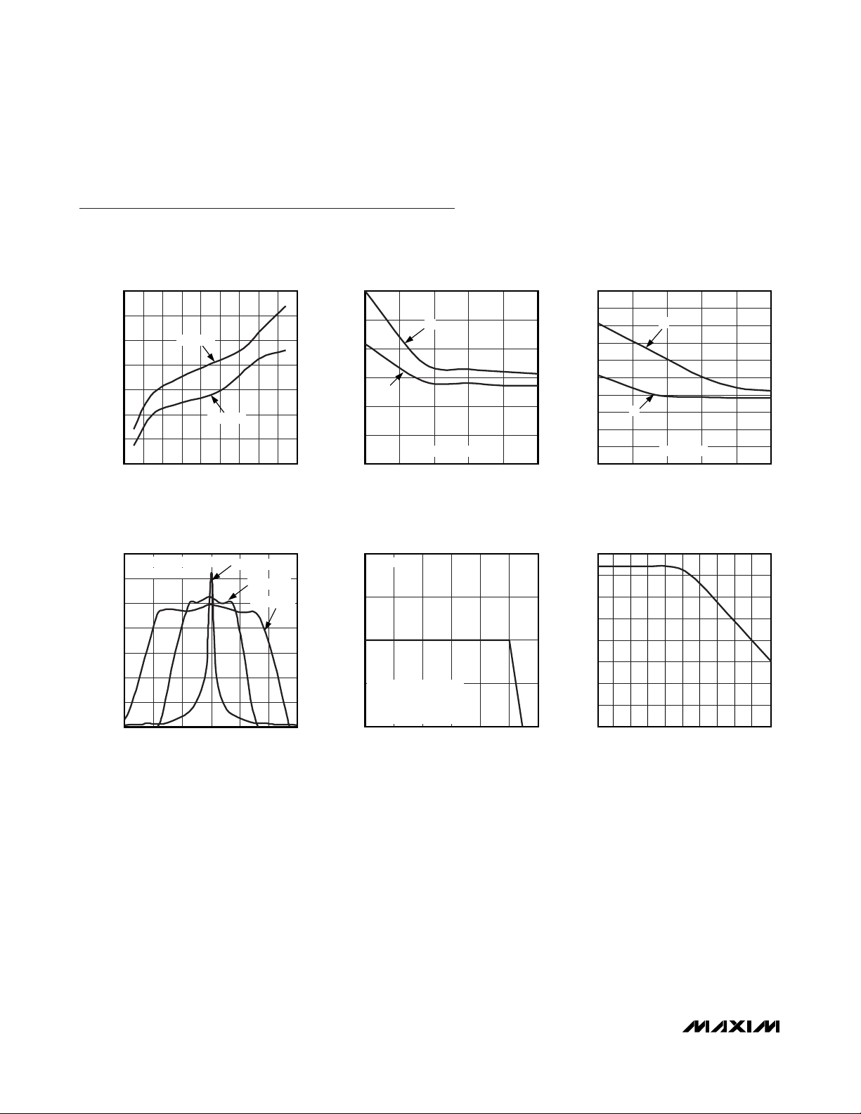
Typical Operating Characteristics
(VCC_ = +3.3V, CL= 8pF, TA= +25°C, unless otherwise noted.)
WORST-CASE PATTERN SUPPLY CURRENT
vs. FREQUENCY
70
60
50
40
30
20
SUPPLY CURRENT (mA)
10
0
04045
OUTPUT POWER SPECTRUM vs. FREQUENCY
0
RESOLUTION BW = 30kHz
VIDEO BW = 100kHz
-10
-20
-30
-40
-50
POWER SPECTRUM (dBm)
-60
-70
39 45
MAX9248
MAX9250
3530510152025
FREQUENCY (MHz)
(REFCLK = 42MHz, NO SPREAD,
4%, AND 2% SPREAD)
NO SPREAD
2% SPREAD
4% SPREAD
43 44424140
FREQUENCY (MHz)
MAX9248/50 toc01
1.00E-14
MAX9248/50 toc04
1.00E-13
1.00E-12
BIT-ERROR RATE
1.00E-11
1.00E-10
OUTPUT TRANSITION TIME
vs. OUTPUT SUPPLY VOLTAGE (V
6
5
4
3
t
2
OUTPUT TRANSITION TIME (ns)
1
0
1.8 3.3
t
R
F
RNG1 = HIGH
OUTPUT SUPPLY VOLTAGE (V)
)
CCO
3.02.72.42.1
10
MAX9248/50 toc02
OUTPUT TRANSITION TIME (ns)
OUTPUT TRANSITION TIME
vs. OUTPUT SUPPLY VOLTAGE (V
9
8
7
6
5
4
t
3
2
1
0
F
1.8 3.3
OUTPUT SUPPLY VOLTAGE (V)
CABLE LENGTH vs. FREQUENCY
BIT-ERROR RATE vs. CABLE LENGTH
MAX9248/50 toc05
FREQUENCY (MHz)
45
40
35
30
25
20
15
10
5
CAT5 CABLE
REFCLK = 42MHz
840Mbps DATA RATE
FOR CABLE LENGTH < 10m
-12
BER < 10
012
CAT5 CABLE LENGTH (m)
810642
BIT-ERROR RATE < 10
t
R
RNG1 = LOW
CABLE LENGTH (m)
)
CCO
MAX9248/50 toc03
3.02.72.42.1
-9
MAX9248/50 toc06
18161412108642020
Page 7

MAX9248/MAX9250
27-Bit, 2.5MHz to 42MHz
DC-Balanced LVDS Deserializers
_______________________________________________________________________________________ 7
Pin Description
PIN
MAX9248 MAX9250
11 R/F
2 2 RNG1
33V
4 4 IN+ Noninverting LVDS Serial-Data Input
5 5 IN- Inverting LVDS Serial-Data Input
6 6 LVDSGND LVDS Supply Ground
7 7 PLLGND PLL Supply Ground
88V
9 9 RNG0
10 10 GND Digital Supply Ground
11 11 V
NAME FUNCTION
Rising or Falling Latch Edge Select. LVTTL/LVCMOS input. Selects the edge of PCLK_OUT
for latching data into the next chip. Set R/F = high for a rising latch edge. Set R/F = low for a
falling latch edge. Internally pulled down to GND.
LVTTL/LVCMOS Range Select Input. Set to the range that includes the serializer parallel
clock input frequency. Internally pulled down to GND.
CCLVDS
CCPLL
CC
LV D S S up p l y V ol tag e. Byp ass to LV D S G N D w i th 0.1µF and 0.001µF cap aci tor s i n p ar al l el as
cl ose to the d evi ce as p ossi b l e, w i th the sm al l est val ue cap aci tor cl osest to the sup p l y p i n.
PLL Supply Voltage. Bypass to PLLGND with 0.1µF and 0.001µF capacitors in parallel as
close to the device as possible with the smallest value capacitor closest to the supply pin.
LVTTL/LVCMOS Range Select Input. Set to the range that includes the serializer parallel
clock input frequency. Internal pulldown to GND.
Digital Supply Voltage. Supply for LVTTL/LVCMOS inputs and digital circuits. Bypass to
GND with 0.1µF and 0.001µF capacitors in parallel as close to the device as possible with
the smallest value capacitor closest to the supply pin.
12 12 REFCLK
13 13 PWRDWN LVTTL/LVCMOS Power-Down Input. Internally pulled down to GND.
14 — SS
15–23 15–23
24 24 DE_OUT
25, 37 25, 37 V
26, 38 26, 38 V
CNTL_OUT0–
CNTL_OUT8
CCOGND
CCO
LVTTL/LVCMOS Reference Clock Input. Apply a reference clock that is within ±2% of the
serializer PCLK_IN frequency. Internally pulled down to GND.
LV TTL/LV C M OS S p r ead - S p ectr um Inp ut. S S sel ects the fr eq uency sp r ead of P C LK_O U T and
outp ut d ata r el ati ve to P C LK_IN . D r i ve S S hi g h for 4% sp r ead and p ul l l ow for 2% sp r ead .
LVTTL/LVCMOS Control Data Outputs. CNTL_OUT[8:0] are latched into the next chip on the
rising or falling edge of PCLK_OUT as selected by R/F when DE_OUT is low, and are held
at the last state when DE_OUT is high.
LVTTL/LVCMOS Data-Enable Output. High indicates RGB_OUT[17:0] are active. Low
indicates CNTL_OUT[8:0] are active.
Output Supply Ground
Output Supply Voltage. Bypass to GND with 0.1µF and 0.001µF capacitors in parallel as
close to the device as possible with the smallest value capacitor closest to the supply pin.
Page 8

MAX9248/MAX9250
27-Bit, 2.5MHz to 42MHz
DC-Balanced LVDS Deserializers
8 _______________________________________________________________________________________
Functional Diagram
Pin Description (continued)
PIN
MAX9248 MAX9250
27 27 LOCK LVTTL/LVCMOS Lock Indicator Output. Outputs are valid when LOCK is low.
28 28 PCLK_OUT LV TTL/LV C M OS P ar al lel Cl ock Outp ut. Latches d ata i nto the next chi p on the ed g e selected b y R/F.
29–36,
39–48
29–36,
39–48
— 14 OUTEN
NAME FUNCTION
RGB_OUT0–
RBG_OUT7,
RGB_OUT8–
RGB_OUT17
LVTTL/LVCMOS Red, Green, and Blue Digital Video Data Outputs. RGB_OUT[17:0] are
latched into the next chip on the edge of PCLK_OUT selected by R/F when DE_OUT is high,
and are held at the last state when DE_OUT is low.
LVTTL/LVCMOS Output Enable Input. High activates the single-ended outputs. Driving
low places the single-ended outputs in high impedance except LOCK. Internally pulled
down to GND.
IN+
IN-
REFCLK
PLL
TIMING AND
CONTROL
DECODE
DC BALANCE/
RNG[0:1]
1
0
SER-TO-PAR
SSPLL
MAX9248
FIFO
R/F
RGB_OUT
CNTL_OUT
DE_OUT
PCLK_OUT
SS
PWRDWN
LOCK
IN+
IN-
REFCLK
PLL
TIMING AND
CONTROL
DECODE
DC BALANCE/
RNG[0:1]
SER-TO-PAR
MAX9250
R/F
1
0
OUTEN
RGB_OUT
CNTL_OUT
DE_OUT
PCLK_OUT
REF_IN
PWRDWN
LOCK
Page 9

MAX9248/MAX9250
27-Bit, 2.5MHz to 42MHz
DC-Balanced LVDS Deserializers
_______________________________________________________________________________________ 9
Figure 5. Synchronous Output Timing
Figure 6. Deserializer Delay
Figure 4. High and Low Times
Figure 3. Output Rise and Fall Times
Figure 1. LVDS Input Bias
Figure 2. Worst-Case Output Pattern
IN+
R
IB
1.2V
R
IB
IN-
DE_OUT
LOCK
PCLK_OUT
RGB_OUT[17:0]
CNTL_OUT[8:0]
t
0.9 x V
0.1 x V
R
PCLK_OUT
CCO
CCO
LVDS
RECEIVER
PCLK_OUT
ODD
RGB_OUT
CNTL_OUT
EVEN
RGB_OUT
CNTL_OUT
RISING LATCH EDGE SHOWN (R/F = HIGH).
PCLK_OUT
t
HIGH
t
F
t
LOW
2.0V
0.8V
2.0V
0.8V
PCLK_OUT SHOWN FOR R/F = HIGH (RISING LATCH EDGE)
DE_OUT
LOCK
RGB_OUT[17:0]
CNTL_OUT[8:0]
20 SERIAL BITS
IN+, IN-
PCLK_OUT
CNTL_OUT
RGB_OUT
SERIAL-WORD N SERIAL-WORD N + 1
0.8V
t
DVB
PCLK_OUT SHOWN FOR R/F = HIGH
t
DELAY
PARALLEL-WORD N - 1 PARALLEL-WORD N
t
DVA
2.0V2.0V
0.8V
Page 10

MAX9248/MAX9250
27-Bit, 2.5MHz to 42MHz
DC-Balanced LVDS Deserializers
10 ______________________________________________________________________________________
Figure 7. PLL Lock to REFCLK and Power-Down Delay for MAX9250
Figure 8. PLL Lock to REFCLK and Power-Down Delay for MAX9248
PWRDWN
REFCLK
0.8V
t
PLLREF
TRANSITION
WORD
FOUND
RECOVERED CLOCK
2.0V
t
PDD
PCLK_OUT
RGB_OUT
CNTL_OUT
DE_OUT
HIGH IMPEDANCE
HIGH IMPEDANCE
LOCK
NOTE: R/F = HIGH
PWRDWN
REFCLK
PCLK_OUT
HIGH IMPEDANCE
HIGH IMPEDANCE
0.8V
t
PLLREF
TRANSITION
WORD
FOUND
CLOCK STRETCH
288 CLOCK CYCLES
VALID DATA
HIGH IMPEDANCE
HIGH IMPEDANCE
HIGH IMPEDANCE
2.0V
t
PDD
OUTPUT CLOCK SPREAD
HIGH IMPEDANCE
OUTPUT DATA SPREAD
VALID DATA
RGB_OUT
CNTL_OUT
DE_OUT
LOCK
NOTE: R/F = HIGH
CLOCK STRETCH
HIGH IMPEDANCE
HIGH IMPEDANCE
HIGH IMPEDANCE
HIGH IMPEDANCE
Page 11

MAX9248/MAX9250
27-Bit, 2.5MHz to 42MHz
DC-Balanced LVDS Deserializers
______________________________________________________________________________________ 11
OUTEN
Figure 9. Output Enable Time
Figure 10. Output Disable Time
Figure 11. Simplified Modulation Profile
DE_OUT
0.8V
OUTEN
MAX9250
t
OE
DE_OUT
2.0V
MAX9250
t
OZ
RGB_OUT[17:0]
CNTL_OUT[8:0]
FREQUENCY
1 / f
SSM
f
(MAX)
RxCLKOUT
f
RxCLKIN
f
(MIN)
RxCLKOUT
ACTIVEHIGH IMPEDANCE
RGB_OUT[17:0]
CNTL_OUT[8:0]
HIGH IMPEDANCEACTIVE
TIME
Page 12

MAX9248/MAX9250
27-Bit, 2.5MHz to 42MHz
DC-Balanced LVDS Deserializers
12 ______________________________________________________________________________________
Detailed Description
The MAX9248/MAX9250 DC-balanced deserializers
operate at a 2.5MHz-to-42MHz parallel clock frequency, deserializing video data to the RGB_OUT[17:0] outputs when the data-enable output DE_OUT is high, or
control data to the CNTL_OUT[8:0] outputs when
DE_OUT is low. The outputs on the MAX9248 are programmable for ±2% or ±4% spread relative to the
LVDS input clock frequency, while the MAX9250 has no
spread, but has an output-enable input that allows output busing. The video phase words are decoded using
two overhead bits, EN0 and EN1. Control phase words
are decoded with one overhead bit, EN0. Encoding,
performed by the MAX9247 serializer, reduces EMI and
maintains DC balance across the serial cable. The serial-input word formats are shown in Tables 1 and 2.
Control data inputs C0 to C4, each repeated over three
serial bit times by the serializer, are decoded using
majority voting. Two or three bits at the same state
determine the state of the recovered bit, providing single bit-error tolerance for C0 to C4. The state of C5 to
C8 is determined by the level of the bit itself (no voting
is used).
AC-Coupling Benefits
AC-coupling increases the input voltage of the LVDS
receiver to the voltage rating of the capacitor. Two
capacitors are sufficient for isolation, but four capacitors—two at the serializer output and two at the deserializer input—provide protection if either end of the
cable is shorted to a high voltage. AC-coupling blocks
low-frequency ground shifts and common-mode noise.
The MAX9247 serializer can also be DC-coupled to the
MAX9248/MAX9250 deserializers. Figures 12 and 14
show the AC-coupled serializer and deserializer with
two capacitors per link, and Figures 13 and 15 show
the AC-coupled serializer and deserializer with four
capacitors per link.
Applications Information
Selection of AC-Coupling Capacitors
See Figure 16 for calculating the capacitor values for
AC-coupling depending on the parallel clock frequency. The plot shows capacitor values for two- and fourcapacitor-per-link systems. For applications using less
than 18MHz clock frequency, use 0.1µF capacitors.
Termination and Input Bias
The IN+ and IN- LVDS inputs are internally connected
to +1.2V through 42kΩ (min) to provide biasing for ACcoupling (Figure 1). Assuming 100Ω interconnect, the
LVDS input can be terminated with a 100Ω resistor.
Match the termination to the differential impedance of
the interconnect.
Use a Thevenin termination, providing 1.2V bias, on an
AC-coupled link in noisy environments. For interconnect with 100Ω differential impedance, pull each LVDS
line up to VCCwith 130Ω and down to ground with 82Ω
at the deserializer input (Figures 12 and 15). This termination provides both differential and common-mode
termination. The impedance of the Thevenin termination
should be half the differential impedance of the interconnect and provide a bias voltage of 1.2V.
Bit 0 is the LSB and is deserialized first. EN[1:0] are encoding bits. S[17:0] are encoded symbols.
Table 1. Serial Video Phase Word Format
Bit 0 is the LSB and is deserialized first. C[8:0] are the mapped control inputs.
Table 2. Serial Control Phase Word Format
012345678910111213141516171819
EN0 EN1 S0 S1 S2 S3 S4 S5 S6 S7 S8 S9 S10 S11 S12 S13 S14 S15 S16 S17
012345678910111213141516171819
E N 0C0C0C0C1C1C1C2C2C2C3C3C3C4C4C4C5C6C7C8
Page 13

MAX9248/MAX9250
27-Bit, 2.5MHz to 42MHz
DC-Balanced LVDS Deserializers
______________________________________________________________________________________ 13
Figure 12. AC-Coupled MAX9247 Serializer and MAX9250 Deserializer with Two Capacitors per Link
Figure 13. AC-Coupled MAX9247 Serializer and MAX9250 Deserializer with Four Capacitors per Link
V
CC
RNG0
RNG1
130Ω
IN
PLL
TIMING AND
CONTROL
DECODE
DC BALANCE/
RGB_IN
CNTL_IN
DE_IN
PCLK_IN
RNG0
RNG1
PWRDWN
PRE
1
0
INPUT LATCH
PLL
ENCODE
DC BALANCE/
TIMING AND
CONTROL
PAR-TO-SER
OUT
CMF
130Ω
*
*
82Ω 82Ω
MAX9247
CERAMIC RF SURFACE-MOUNT CAPACITOR
100Ω DIFFERENTIAL STP CABLE
*CAPACITORS CAN BE AT EITHER END.
SER-TO-PAR
MAX9250
R/F
1
0
OUTEN
RGB_OUT
CNTL_OUT
DE_OUT
PCLK_OUT
REF_IN
PWRDWN
LOCK
V
CC
RNG0
RNG1
130Ω
IN
PLL
TIMING AND
CONTROL
DECODE
DC BALANCE/
RGB_IN
CNTL_IN
DE_IN
PCLK_IN
RNG0
RNG1
PWRDWN
PRE
1
0
INPUT LATCH
PLL
ENCODE
DC BALANCE/
TIMING AND
CONTROL
PAR-TO-SER
OUT
CMF
130Ω
82Ω 82Ω
MAX9247
CERAMIC RF SURFACE-MOUNT CAPACITOR
100Ω DIFFERENTIAL STP CABLE
SER-TO-PAR
MAX9250
R/F
1
0
OUTEN
RGB_OUT
CNTL_OUT
DE_OUT
PCLK_OUT
REF_IN
PWRDWN
LOCK
Page 14

MAX9248/MAX9250
27-Bit, 2.5MHz to 42MHz
DC-Balanced LVDS Deserializers
14 ______________________________________________________________________________________
Figure 14. AC-Coupled MAX9247 Serializer and MAX9248 Deserializer with Two Capacitors per Link
Figure 15. AC-Coupled MAX9247 Serializer and MAX9248 Deserializer with Four Capacitors per Link
V
CC
130Ω
REFCLK
IN+
IN-
PLL
TIMING AND
CONTROL
RGB_IN
CNTL_IN
DE_IN
PCLK_IN
RNG0
RNG1
PWRDWN
PRE
1
0
INPUT LATCH
PLL
ENCODE
DC BALANCE/
TIMING AND
CONTROL
PAR-TO-SER
OUT
CMF
130Ω
*
*
82Ω 82Ω
MAX9247
CERAMIC RF SURFACE-MOUNT CAPACITOR
*CAPACITORS CAN BE AT EITHER END.
130Ω
82Ω 82Ω
RGB_IN
CNTL_IN
DE_IN
PRE
1
0
INPUT LATCH
ENCODE
DC BALANCE/
PAR-TO-SER
OUT
CMF
100Ω DIFFERENTIAL STP CABLE
V
CC
130Ω
IN+
IN-
DECODE
DC BALANCE/
RNG[0:1]
DECODE
DC BALANCE/
1
0
SER-TO-PAR
SSPLL
MAX9248
1
0
SER-TO-PAR
FIFO
FIFO
R/F
RGB_OUT
CNTL_OUT
DE_OUT
PCLK_OUT
SS
PWRDWN
LOCK
R/F
RGB_OUT
CNTL_OUT
DE_OUT
PCLK_OUT
PCLK_IN
RNG0
RNG1
PWRDWN
PLL
TIMING AND
CONTROL
MAX9247
CERAMIC RF SURFACE-MOUNT CAPACITOR
REFCLK
100Ω DIFFERENTIAL STP CABLE
PLL
TIMING AND
CONTROL
SSPLL
MAX9248
RNG[0:1]
SS
PWRDWN
LOCK
Page 15

MAX9248/MAX9250
27-Bit, 2.5MHz to 42MHz
DC-Balanced LVDS Deserializers
______________________________________________________________________________________ 15
Input Frequency Detection
A frequency-detection circuit detects when the LVDS
input is not switching. When not switching, all outputs
except LOCK are low, LOCK is high, and PCLK_OUT
follows REFCLK. This condition occurs, for example, if
the serializer is not driving the interconnect or if the
interconnect is open.
Frequency Range Setting (RNG[1:0])
The RNG[1:0] inputs select the operating frequency
range of the MAX9248/MAX9250 and the transition time
of the outputs. Select the frequency range that includes
the MAX9247 serializer PCLK_IN frequency. Table 3
shows the selectable frequency ranges and the corresponding data rates and output transition times.
Power Down
Driving PWRDWN low puts the outputs in high impedance and stops the PLL. With PWRDWN ≤ 0.3V and all
LVTTL/LVCMOS inputs ≤ 0.3V or ≥ VCC- 0.3V, the supply current is reduced to less than 50µA. Driving
PWRDWN high initiates lock to the local reference clock
(REFCLK) and afterwards to the serial input.
Lock and Loss-of-Lock (
LOCK
)
When PWRDWN is driven high, the PLL begins locking
to REFCLK, drives LOCK from high impedance to high
and the other outputs from high impedance to low,
except PCLK_OUT. PCLK_OUT outputs REFCLK while
the PLL is locking to REFCLK. Lock to REFCLK takes a
maximum of 16,928 REFCLK cycles for the MAX9250.
The MAX9248 has an additional spread-spectrum PLL
(SSPLL) that also begins locking to REFCLK. Locking
both PLLs to REFCLK takes a maximum of 33,600 REFCLK
cycles for the MAX9248.
When the MAX9248/MAX9250 complete their lock to
REFCLK, the serial input is monitored for a transition
word. When a transition word is found, LOCK output is
driven low, indicating valid output data and the parallel
rate clock recovered from the serial input is output on
PCLK_OUT. The MAX9248 SSPLL waits an additional
288 clock cycles after the transition word is found
before LOCK is driven low and sequence takes effect.
PCLK_OUT is stretched on the change from REFCLK to
recovered clock (or vice versa) at the time when the
transition word is found.
If a transition word is not detected within 2
22
cycles of
PCLK_OUT, LOCK is driven high, the other outputs
except PCLK_OUT are driven low. REFCLK is output on
PCLK_OUT and the deserializer continues monitoring
the serial input for a transition word. See Figure 7 for
the MAX9250 and Figure 8 for the MAX9248 regarding
the synchronization timing diagram.
The MAX9248 input-to-output delay can be as low as
(4.5tT+ 8.0)ns or as high as (36tT+ 16)ns due to
spread-spectrum variations (see Figure 6).
The MAX9250 input-to-output delay can be as low as
(3.575tT+ 8)ns or as high as (3.725tT+ 16)ns.
Figure 16. AC-Coupling Capacitor Values vs. Clock Frequency
of 18MHz to 42MHz
Table 3. Frequency Range Programming
PARALLEL
RNG1 RNG0
0 0 2.5 to 5.0 50 to 100
0 1 5 to 10 100 to 200
1 0 10 to 20 200 to 400
1 1 20 to 42 400 to 840
CLOCK
(MHz)
SERIAL-
DATA RATE
(Mbps)
OUTPUT
TRANSITION
TIME
Slow
Fast
140
120
100
80
60
40
CAPACITOR VALUE (nF)
20
0
18 42
FOUR CAPACITORS PER LINK
TWO CAPACITORS PER LINK
21 24 27 33 36 3930
PARALLEL CLOCK FREQUENCY (MHz)
Page 16

MAX9248/MAX9250
27-Bit, 2.5MHz to 42MHz
DC-Balanced LVDS Deserializers
16 ______________________________________________________________________________________
Spread-Spectrum Selection
The MAX9248 single-ended data and clock outputs are
programmable for a variation of ±2% or ±4% around
the LVDS input clock frequency. The modulation rate of
the frequency variation is 32kHz for a 33MHz LVDS
clock input and scales linearly with the clock frequency
(see Table 4). The output spread is controlled through
the SS input (see Table 5). Driving SS high spreads all
data and clock outputs by ±4%, while pulling low
spreads ±2%.
Any spread change causes a delay time of 32,000 x t
T
before output data is valid. When the spread amount is
changed from ±2% to ±4% or vice versa, the data outputs go low for one t
ΔSSPLL
delay (see Figure 17). The
data outputs stay low, but are not valid when the
spread amount is changed.
Output Enable (OUTEN) and
Busing Outputs
The outputs of two MAX9250s can be bused to form a
2:1 mux with the outputs controlled by the output
enable. Wait 30ns between disabling one deserializer
(driving OUTEN low) and enabling the second one (driving OUTEN high) to avoid contention of the bused outputs. OUTEN controls all outputs except LOCK.
Rising or Falling Output Latch Edge (R/F)
The MAX9248/MAX9250 have a selectable rising or
falling output latch edge through a logic setting on R/F.
Driving R/F high selects the rising output latch edge,
which latches the parallel output data into the next chip
on the rising edge of PCLK_OUT. Driving R/F low
selects the falling output latch edge, which latches the
parallel output data into the next chip on the falling
edge of PCLK_OUT. The MAX9248/MAX9250 outputlatch-edge polarity does not need to match the
MAX9247 serializer input-latch-edge polarity. Select the
latch-edge polarity required by the chip being driven
by the MAX9248/MAX9250.
Figure 17. Output Waveforms when Spread Amount is Changed
Table 4. Modulation Rate
Table 5. SS Function
f
PCLK_IN
8 7.81
10 9.77
16 15.63
32 31.25
40 39.06
42 41.01
fM(kHz) = f
PCLK_IN
SS INPUT LEVEL OUTPUT SPREAD
High
Low
Data and clock output spread ±4%
relative to REFCLK
Data and clock output spread ±2%
relative to REFCLK
/ 1024
SS
PCLK_OUT
RGB_OUT[17:0]
CNTL_OUT8:0]
LOCK
±4% OR ±2% SPREAD±4% OR ±2% SPREAD
t
ΔSSPLL
(32,800 x tT)
LOW
Page 17

MAX9248/MAX9250
27-Bit, 2.5MHz to 42MHz
DC-Balanced LVDS Deserializers
______________________________________________________________________________________ 17
Staggered and Transition Time
Adjusted Outputs
RGB_OUT[17:0] are grouped into three groups of six, with
each group switching about 1ns apart in the video phase
to reduce EMI and ground bounce. CNTL_OUT[8:0]
switch during the control phase. Output transition times
are slower in the 2.5MHz to 5MHz and 5MHz to 10MHz
ranges and faster in the 10MHz to 20MHz and 20MHz to
42MHz ranges.
Data-Enable Output (DE_OUT)
The MAX9248/MAX9250 deserialize video and control
data at different times. Control data is deserialized during
the video blanking time. DE_OUT high indicates that
video data is being deserialized and output on
RGB_OUT[17:0]. DE_OUT low indicates that control data
is being deserialized and output on CNTL_OUT[8:0].
When outputs are not being updated, the last data
received is latched on the outputs. Figure 18 shows the
DE_OUT timing.
Power-Supply Sequencing of MAX9247
and MAX9248/MAX9250 Video Link
The MAX9247 and MAX9248/MAX9250 video link can
be powered up in several ways. The best approach is
to keep both MAX9247 and MAX9248 powered down
while supplies are ramping up and PCLK_IN of the
MAX9247 and REFCLK of the MAX9248/MAX9250 are
stabilizing. After all of the power supplies of the
MAX9247 and MAX9248/MAX9250 are stable, including
PCLK_IN and REFCLK, do the following:
• Power up the MAX9247 first
• Wait for at least t
LOCK
of MAX9247 (or 17100 x tT)
to get activity on the link
• Power up the MAX9248
Power-Supply Circuits and Bypassing
There are separate on-chip power domains for digital
circuits and LVTTL/LVCMOS inputs (V
CC
supply and
GND), outputs (V
CCO
supply and V
CCOGND
), PLL
(V
CCPLL
supply and PLLGND), and the LVDS input
(V
CCLVDS
supply and LVDSGND). The grounds are iso-
lated by diode connections. Bypass each VCC, V
CCO
,
V
CCPLL
, and V
CCLVDS
pin with high-frequency, surface-mount ceramic 0.1µF and 0.001µF capacitors in
parallel as close to the device as possible, with the
smallest value capacitor closest to the supply pin. The
outputs are powered from V
CCO
, which accepts a
1.71V to 3.6V supply, allowing direct interface to inputs
with 1.8V to 3.3V logic levels.
Cables and Connectors
Interconnect for LVDS typically has a differential
impedance of 100Ω. Use cables and connectors that
have matched differential impedance to minimize
impedance discontinuities.
Twisted-pair and shielded twisted-pair cables offer
superior signal quality compared to ribbon cable and
tend to generate less EMI due to magnetic field canceling effects. Balanced cables pick up noise as common
mode, which is rejected by the LVDS receiver.
Figure 18. Output Timing
CONTROL DATA
PCLK_OUT
CNTL_OUT
DE_OUT
RGB_OUT
= OUTPUT DATA HELD
CONTROL DATAVIDEO DATA
PCLK_OUT TIMING SHOWN FOR R/F = HIGH (RISING OUTPUT LATCH EDGE)
Page 18

MAX9248/MAX9250
27-Bit, 2.5MHz to 42MHz
DC-Balanced LVDS Deserializers
18 ______________________________________________________________________________________
Board Layout
Separate the LVTTL/LVCMOS outputs and LVDS inputs
to prevent crosstalk. A four-layer PCB with separate layers for power, ground, and signals is recommended.
ESD Protection
The MAX9248/MAX9250 ESD tolerance is rated for
Human Body Model, Machine Model, IEC 61000-4-2 and
ISO 10605. The ISO 10605 and IEC 61000-4-2 standards
specify ESD tolerance for electronic systems. All LVDS
inputs on the MAX9248/MAX9250 meet ISO 10605 ESD
protection at ±30kV Air-Gap Discharge and ±10kV
Contact Discharge and IEC 61000-4-2 ESD protection at
±15kV Air-Gap Discharge and ±10kV Contact
Discharge. All other pins meet the Human Body Model
ESD tolerance of ±2kV. The Human Body Model discharge components are CS= 100pF and RD= 1.5kΩ
(Figure 19). The IEC 61000-4-2 discharge components
are CS= 150pF and RD= 330Ω (see Figure 20). The ISO
10605 discharge components are C
S
= 330pF and RD=
2kΩ (Figure 21). The Machine Model discharge components are C
S
= 200pF and RD= 0Ω (Figure 22).
RGB_OUT7
RGB_OUT6
RGB_OUT5
RGB_OUT4
RGB_OUT3
RGB_OUT2
RGB_OUT1
RGB_OUT0
PCLK_OUT
LOCK
V
CCO
V
CCOGND
1
2
3
4
5
6
7
8
9
10
11
12
36
35
34
33
32
31
30
29
28
27
26
25
PWRDWN
SS (OUTEN)
CNTL_OUT0
CNTL_OUT1
CNTL_OUT2
CNTL_OUT3
CNTL_OUT4
CNTL_OUT5
CNTL_OUT6
CNTL_OUT7
CNTL_OUT8
DE_OUT
LQFP
MAX9248/MAX9250
1314151617181920212223
24
4847464544434241403938
37
RGB_OUT17
RGB_OUT16
RGB_OUT15
RGB_OUT14
RGB_OUT13
RGB_OUT12
RGB_OUT11
RGB_OUT10
RGB_OUT9
RGB_OUT8
V
CCOVCCOGND
R/F
RNG1
V
CCLVDS
IN+
IN-
LVDSGND
PLLGND
V
CCPLL
RNG0
GND
V
CC
REFCLK
TOP VIEW
Pin Configuration
Figure 19. Human Body ESD Test Circuit
Figure 20. IEC 61000-4-2 Contact Discharge ESD Test Circuit
Figure 21. ISO 10605 Contact Discharge ESD Test Circuit
Figure 22. Machine Model ESD Test Circuit
R
D
1.5kΩ
DISCHARGE
RESISTANCE
C
S
STORAGE
CAPACITOR
HIGH-
VOLTAGE
DC
SOURCE
1MΩ
CHARGE-CURRENT-
LIMIT RESISTOR
100pF
R
D
2kΩ
CHARGE-CURRENT-
DC
LIMIT RESISTOR
330pF
HIGH-
VOLTAGE
SOURCE
DISCHARGE
RESISTANCE
C
S
STORAGE
CAPACITOR
DEVICE
UNDER
TEST
DEVICE
UNDER
TEST
R2
330Ω
HIGH-
VOLTAGE
DC
SOURCE
CHARGE-CURRENT-
LIMIT RESISTOR
150pF
DISCHARGE
RESISTANCE
C
S
STORAGE
CAPACITOR
DEVICE
UNDER
TEST
R
D
0Ω
HIGH-
VOLTAGE
DC
SOURCE
CHARGE-CURRENT-
LIMIT RESISTOR
200pF
C
S
DISCHARGE
RESISTANCE
STORAGE
CAPACITOR
DEVICE
UNDER
TEST
Page 19

MAX9248/MAX9250
27-Bit, 2.5MHz to 42MHz
DC-Balanced LVDS Deserializers
______________________________________________________________________________________ 19
Package Information
For the latest package outline information and land patterns, go
to www.maxim-ic.com/packages
.
PACKAGE TYPE PACKAGE CODE DOCUMENT NO.
48 LQFP C48+3
21-0054
Chip Information
PROCESS: CMOS
Page 20
Revision History
27-Bit, 2.5MHz to 42MHz
DC-Balanced LVDS Deserializers
MAX9248/MAX9250
Maxim cannot assume responsibility for use of any circuitry other than circuitry entirely embodied in a Maxim product. No circuit patent licenses are
implied. Maxim reserves the right to change the circuitry and specifications without notice at any time.
20
____________________Maxim Integrated Products, 120 San Gabriel Drive, Sunnyvale, CA 94086 408-737-7600
© 2009 Maxim Integrated Products Maxim is a registered trademark of Maxim Integrated Products, Inc.
REVISION
NUMBER
2 5/08
3 4/09
REVISION
DATE
DESCRIPTION
Rep l aced TQFP and TQFN p ackag es w i th LQ FP p ackag e, chang ed tem p er atur e
l i m i ts for + 105° C p ar t, and ad d ed M achi nes M od el E S D text and d i ag r am
Added /V parts in the Ordering Information table and added new Power-
S up p l y S eq uenci ng of M AX 9247 and M AX 9248/M AX 9250 V i d eo Li nk secti on
PAGES
CHANGED
1–5, 7, 16–19
1, 17
 Loading...