

Page 1
General Description
The MAX9247 digital video parallel-to-serial converter
serializes 27 bits of parallel data into a serial-data stream.
Eighteen bits of video data and 9 bits of control data are
encoded and multiplexed onto the serial interface, reducing the serial-data rate. The data-enable input determines
when the video or control data is serialized.
The MAX9247 pairs with the MAX9248/MAX9250 deserializers to form a complete digital video serial link.
Interconnect can be controlled-impedance PCB traces or
twisted-pair cable. Proprietary data encoding reduces
EMI and provides DC balance. DC balance allows ACcoupling, providing isolation between the transmitting
and receiving ends of the interface. The LVDS output is
internally terminated with 100Ω. For operating frequencies less than 35MHz, the MAX9247 can also pair with
the MAX9218 deserializer.
ESD tolerance is specified for ISO 10605 with ±10kV
Contact Discharge and ±30kV Air-Gap Discharge.
The MAX9247 operates from a +3.3V core supply and
features a separate input supply for interfacing to 1.8V
to 3.3V logic levels. This device is available in a 48-lead
LQFP package and is specified from -40°C to +85°C or
-40°C to +105°C.
Applications
Navigation System Displays
In-Vehicle Entertainment Systems
Video Cameras
LCDs
Features
o Preemphasis Improves Eye Diagram and Signal
Integrity at the Output
o Proprietary Data Encoding for DC Balance and
Reduced EMI
o Control Data Sent During Video Blanking
o Five Control Data Inputs are Single-Bit-Error
Tolerant
o Programmable Phase-Shifted LVDS Signaling
Reduces EMI
o Output Common-Mode Filter Reduces EMI
o Greater Than 10m STP Cable Drive
o Wide ±2% Reference Clock Tolerance
o ISO 10605 and IEC 61000-4-2 Level 4
ESD Protection
o Separate Input Supply Allows Interface to 1.8V
to 3.3V Logic
o +3.3V Core Supply
o Space-Saving LQFP Package
o -40°C to +85°C and -40°C to +105°C Operating
Temperature Ranges
MAX9247
________________________________________________________________
Maxim Integrated Products
1
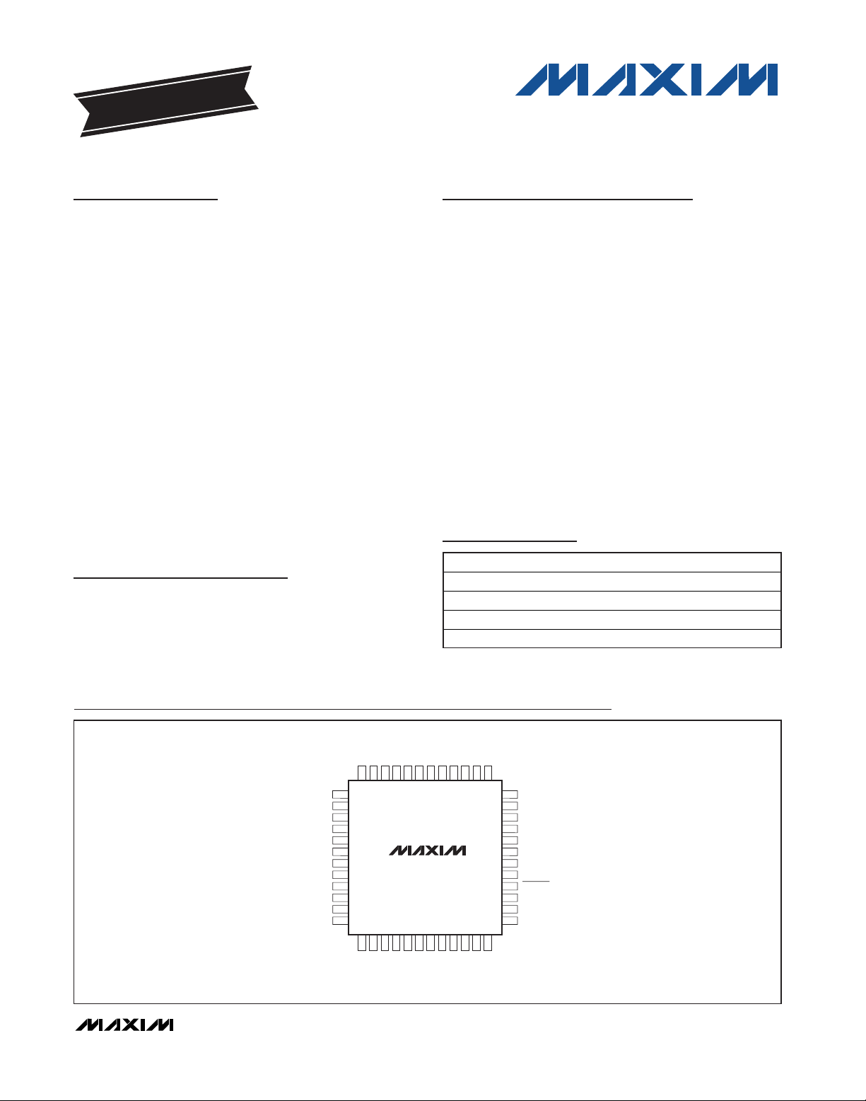
Pin Configuration
Ordering Information
19-3955; Rev 4; 4/12
For pricing, delivery, and ordering information, please contact Maxim Direct at 1-888-629-4642,
or visit Maxim’s website at www.maxim-ic.com.
EVALUATION KIT
AVAILABLE
+
Denotes a lead(Pb)-free/RoHS-compliant package.
/V denotes an automotive qualified part.
27-Bit, 2.5MHz-to-42MHz
DC-Balanced LVDS Serializer
PART TEMP RANGE PIN-PACKAGE
MAX9247ECM+ -40°C to +85°C 48 LQFP
MAX9247ECM/V+ -40°C to +85°C 48 LQFP
MAX9247GCM+ -40°C to +105°C 48 LQFP
MAX9247GCM/V+ -40°C to +105°C 48 LQFP
TOP VIEW
GND
V
CCIN
RGB_IN10
RGB_IN11
RGB_IN12
RGB_IN13
RGB_IN14
RGB_IN15
RGB_IN16
RGB_IN17
CNTL_IN0
CNTL_IN1
RGB_IN9
RGB_IN8
RGB_IN7
RGB_IN6
RGB_IN5
4847464544434241403938
+
1
2
3
4
5
6
7
8
9
10
11
12
1314151617181920212223
GND
CC
V
CNTL_IN3
CNTL_IN2
MAX9247
CNTL_IN4
LQFP
RGB_IN4
RGB_IN3
CNTL_IN5
CNTL_IN6
RGB_IN2
RGB_IN1
CNTL_IN7
CNTL_IN8
RGB_IN0
VCCGND
DE_IN
PCLK_IN
37
36
RNG0
RNG1
35
V
34
CCLVDS
OUT+
33
OUT-
32
LVDSGND
31
LVDSGND
30
CMF
29
PWRDWN
28
V
27
CCPLL
PLLGND
26
PRE
25
24
I.C.
Page 2
MAX9247
27-Bit, 2.5MHz-to-42MHz
DC-Balanced LVDS Serializer
2 _______________________________________________________________________________________
ABSOLUTE MAXIMUM RATINGS
DC ELECTRICAL CHARACTERISTICS
(V
CC_
= +3.0V to +3.6V, RL= 100Ω ±1%, PWRDWN = high, PRE = low, TA= -40°C to +105°C, unless otherwise noted. Typical
values are at V
CC_
= +3.3V, TA= +25°C.) (Notes 1, 2)
Stresses beyond those listed under “Absolute Maximum Ratings” may cause permanent damage to the device. These are stress ratings only, and functional
operation of the device at these or any other conditions beyond those indicated in the operational sections of the specifications is not implied. Exposure to
absolute maximum rating conditions for extended periods may affect device reliability.
V
CC_
to _GND........................................................-0.5V to +4.0V
Any Ground to Any Ground...................................-0.5V to +0.5V
OUT+, OUT-, CMF to LVDSGND...........................-0.5V to +4.0V
OUT+, OUT- Short Circuit to LVDSGND
or V
CCLVDS
.............................................................Continuous
OUT+, OUT- Short Through 0.125µF (or smaller),
25V Series Capacitor..........................................-0.5V to +16V
RGB_IN[17:0], CNTL_IN[8:0], DE_IN,
RNG0, RNG1, PRE, PCLK_IN,
PWRDWN to GND ...............................-0.5V to (V
CCIN
+ 0.5V)
Continuous Power Dissipation (T
A
= +70°C)
48-Lead LQFP (derate 20.8mW/°C above +70°C)....1666.7mW
ESD Protection
Machine Model (R
D
= 0Ω, CS= 200pF)
All Pins to GND ..............................................................±200V
Human Body Model (R
D
= 1.5kΩ, CS= 100pF)
All Pins to GND ................................................................±3kV
ISO 10605 (R
D
= 2kΩ, CS= 330pF)
Contact Discharge (OUT+, OUT-) to LVDSGND ...........±10kV
Air-Gap Discharge (OUT+, OUT-) to LVDSGND ...........±30kV
IEC 61000-4-2 (R
D
= 330Ω, CS= 150pF)
Contact Discharge (OUT+, OUT-) to LVDSGND ...........±10kV
Air-Gap Discharge (OUT+, OUT-) to LVDSGND ...........±15kV
Storage Temperature Range .............................-65°C to +150°C
Junction Temperature......................................................+150°C
Lead Temperature (soldering,10s)..................................+300°C
Soldering Temperature (reflow) .......................................+260°C
PARAMETER SYMBOL CONDITIONS MIN TYP MAX UNITS
SINGLE-ENDED INPUTS (RGB_IN[17:0], CNTL_IN[8:0], DE_IN, PCLK_IN, PWRDWN, RNG_, PRE)
High-Level Input Voltage V
Low-Level Input Voltage V
Input Current I
Input Clamp Voltage V
LVDS OUTPUTS (OUT+, OUT-)
Differential Output Voltage V
Change in VOD Between
Complementary Output States
Common-Mode Voltage V
Change in VOS Between
Complementary Output States
Output Short-Circuit Current I
Magnitude of Differential
Output Short-Circuit Current
Output High-Impedance
Current
IH
IL
IN
CL
OD
∆V
OD
OS
∆V
OS
OS
I
OSD
I
OZ
V
= 1.71V to < 3V (Note 3) 0.65 x V
CCIN
V
= 3.0V to 3.6V 2 0.3 + V
CCIN
V
= 1.71V to < 3V (Note 3) -0.3 0.3 x V
CCIN
V
= 3.0V to 3.6V -0.3 +0.8
CCIN
V
= 1.71V
CCIN
to 3.6V,
PWRDWN =
high or low
VIN = -0.3V to 0V
(MAX9247ECM),
V
(MAX9247GCM)
V
ICL = -18mA -1.5 V
Figure 1 250 335 450 mV
Figure 1 20 mV
Figure 1 1.125 1.29 1.475 V
Figure 1 20 mV
V
or V
OUT+
V
= 0V 5.5 15 mA
OD
= 0V or 3.6V -15 ±8 +15 mA
OUT-
PWRDWN = low
or V
CC_
= 0V
V
CCIN
+ 0.3
CCIN
CCIN
= -0.15V to 0V
IN
= 0V to ( V
IN
V
OUT+
V
OUT-
V
OU T +
V
OUT-
CCIN
-100 +20
+ 0.3V) -20 +20
C C IN
= 0V,
= 3.6V
= 3.6V ,
-1 +1 µA
= 0V
V
V
µA
Page 3
MAX9247
27-Bit, 2.5MHz-to-42MHz
DC-Balanced LVDS Serializer
_______________________________________________________________________________________ 3
AC ELECTRICAL CHARACTERISTICS
(V
CC_
= +3.0V to +3.6V, RL= 100Ω ±1%, CL= 5pF, PWRDWN = high, PRE = low, TA= -40°C to +105°C, unless otherwise noted.
Typical values are at V
CC_
= +3.3V, TA= +25°C.) (Note 3)
DC ELECTRICAL CHARACTERISTICS (continued)
(V
CC_
= +3.0V to +3.6V, RL= 100Ω ±1%, PWRDWN = high, PRE = low, TA= -40°C to +105°C, unless otherwise noted. Typical
values are at V
CC_
= +3.3V, TA= +25°C.) (Notes 1, 2)
PARAMETER SYMBOL CONDITIONS MIN TYP MAX UNITS
Differential Output Resistance R
Worst-Case Supply Current
Power-Down Supply Current I
O
I
CCW
CCZ
78 110 147 Ω
2.5MHz
5MHz
RL = 100Ω ±1%,
C
= 5pF,
L
continuous 10
transition words
(Note 4) 50 µA
10MHz
20MHz
35MHz
42MHz
PRE = 0 15 25
PRE = 1 27
PRE = 0 18 25
PRE = 1 27
PRE = 0 23 28
PRE = 1 30
PRE = 0 33 39
PRE = 1 42
PRE = 0 50 65
PRE = 1 69
PRE = 0 60 70
PRE = 1 75
PARAMETER SYMBOL CONDITIONS MIN TYP MAX UNITS
PCLK_IN TIMING REQUIREMENTS
Clock Period t
Clock Frequency f
Clock Frequency Difference from
Deserializer Reference Clock
Clock Duty Cycle DC t
Clock Transition Time tR, t
SWITCHING CHARACTERISTICS
Output Rise Time t
Output Fall Time t
Input Setup Time t
Input Hold Time t
T
CLK
∆f
CLK
F
RISE
FALL
SET
HOLD
Figure 2
MAX9247ECM 2.5 42.0
MAX9247GCM 2.5 35.0
or t
HIGH/tT
Figure 2 2.5 ns
20% to 80%,
V
OD
80% to 20%,
V
OD
Figure 4 3 ns
Figure 4 3 ns
LOW
≥ 250mV, Figure 3
≥ 250mV, Figure 3
MAX9247ECM 23.8 400.0
MAX9247GCM 28.6 400.0
-2 +2 %
/tT, Figure 2 35 50 65 %
PRE = low 280 370
PRE = high 240 320
PRE = low 280 370
PRE = high 240 320
mA
ns
MHz
ps
ps
Page 4
MAX9247
27-Bit, 2.5MHz-to-42MHz
DC-Balanced LVDS Serializer
4 _______________________________________________________________________________________
AC ELECTRICAL CHARACTERISTICS (continued)
(V
CC_
= +3.0V to +3.6V, RL= 100Ω±1%, CL= 5pF, PWRDWN = high, PRE = low, TA= -40°C to +105°C, unless otherwise noted.
Typical values are at V
CC_
= +3.3V, TA= +25°C.) (Note 3)
)
Note 1: Current into a pin is defined as positive. Current out of a pin is defined as negative. All voltages are referenced to ground,
except V
OD
, ∆VOD, and ∆VOS.
Note 2: Maximum and minimum limits over temperature are guaranteed by design and characterization. Devices are production
tested at T
A
= +25°C.
Note 3: Parameters are guaranteed by design and characterization and are not production tested. Limits are set at ±6 sigma.
Note 4: All LVTTL/LVCMOS inputs, except PWRDWN at ≤ 0.3V or ≥ V
CCIN
- 0.3V. PWRDWN is ≤ 0.3V.
PARAMETER SYMBOL CONDITIONS MIN TYP MAX UNITS
Serializer Delay t
PLL Lock Time t
Power-Down Delay t
Peak-to-Peak Output Jitter t
Peak-to-Peak Output Offset
Voltage
LOCK
JITT
V
OS(P-P
SD
PD
Figure 5
Figure 6
Figure 7 1 µs
Measured with PRBS input pattern at
840Mbps data rate
840Mbps data rate,
CMF open, Figure 8
840Mbps data rate,
CMF 0.1µF to ground, Figure 8
3.10 x
+ 2.0
t
T
22 70
12 50
3.10 x
tT + 8.0
17,100 x
t
T
150 ps
ns
ns
mV
Page 5

MAX9247
27-Bit, 2.5MHz-to-42MHz
DC-Balanced LVDS Serializer
_______________________________________________________________________________________ 5
Typical Operating Characteristics
(V
CC_
= +3.3V, RL= 100Ω, TA = +25°C, unless otherwise noted.)
WORST-CASE PATTERN
SUPPLY CURRENT vs. FREQUENCY
70
60
50
40
30
SUPPLY CURRENT (mA)
20
10
0
WITH PREEMPHASIS
0
WITHOUT PREEMPHASIS
FREQUENCY (MHz)
MAX9247 toc01
100mV/div
40302010
BIT-ERROR RATE vs. CABLE LENGTH
1.00E-14
1.00E-13
1.00E-12
BIT-ERROR RATE
1.00E-11
1.00E-10
CAT5 CABLE
f
= 42MHz
REFCLK
840Mbps DATA RATE
FOR CABLE LENGTH < 10m
-12
BER < 10
0
CAT5 CABLE LENGTH (m)
EYE DIAGRAM WITHOUT PREEMPHASIS
GND
200ps/div
MAX9247 toc04
2 METER CAT5 CABLE
100Ω TERMINATION
vs. FREQUENCY BIT-ERROR RATE < 10
45
40
35
30
25
20
FREQUENCY (MHz)
15
10
5
81012642
PRE = LOW
f
= 42MHz
REFCLK
MAX9247 toc02
100mV/div
CABLE LENGTH
CABLE LENGTH (m)
EYE DIAGRAM WITH PREEMPHASIS
PRE = HIGH
f
= 42MHz
REFCLK
2 METER CAT5 CABLE
100Ω TERMINATION
GND
200ps/div
-9
MAX9247 toc05
18161412108642020
MAX9247 toc03
Page 6
MAX9247
27-Bit, 2.5MHz-to-42MHz
DC-Balanced LVDS Serializer
6 _______________________________________________________________________________________
Pin Description
PIN NAME FUNCTION
1, 13, 37 GND Input Buffer Supply and Digital Supply Ground
2V
RGB_IN10–
3–10,
39–48
11, 12, 15–21
14, 38 V
22 DE_IN
23 PCLK_IN
24 I.C. Internally Connected. Leave unconnected for normal operation.
25 PRE Preemphasis Enable Input. Drive PRE high to enable preemphasis.
26 PLLGND PLL Supply Ground
27 V
28 PWRDWN LVTTL/LVCMOS Power-Down Input. Internally pulled down to GND.
29 CMF
30, 31 LVDSGND LVDS Supply Ground
32 OUT- Inverting LVDS Serial-Data Output
33 OUT+ Noninverting LVDS Serial-Data Output
34 V
35 RNG1
36 RNG0
RGB_IN17,
RGB_IN0–
CNTL_IN0,
CNTL_IN1,
CNTL_IN2–
CNTL_IN8
CCIN
RGB_IN9
CC
CCPLL
CCLVDS
Input Buffer Supply Voltage. Bypass to GND with 0.1µF and 0.001µF capacitors in parallel as
close to the device as possible, with the smallest value capacitor closest to the supply pin.
LVTTL/LVCMOS Red, Green, and Blue Digital Video Data Inputs. Eighteen data bits are loaded
into the input latch on the rising edge of PCLK_IN when DE_IN is high. Internally pulled down to
GND.
LVTTL/LVCMOS Control Data Inputs. Control data are latched on the rising edge of PCLK_IN
when DE_IN is low. Internally pulled down to GND.
Digital Supply Voltage. Bypass to GND with 0.1µF and 0.001µF capacitors in parallel as close to
the device as possible, with the smallest value capacitor closest to the supply pin.
LVTTL/LVCMOS Data-Enable Input. Logic-high selects RGB_IN[17:0] to be latched. Logic-low
selects CNTL_IN[8:0] to be latched. DE_IN must be switching for proper operation. Internally
pulled down to GND.
LVTTL/LVCMOS Parallel Clock Input. Latches data and control inputs and provides the PLL
reference clock. Internally pulled down to GND.
PLL Supply Voltage. Bypass to PLLGND with 0.1µF and 0.001µF capacitors in parallel as close to
the device as possible, with the smallest value capacitor closest to the supply pin.
Common-Mode Filter. Optionally connect a capacitor between CMF and LVDSGND to filter
common-mode switching noise.
LVDS Supply Voltage. Bypass to LVDSGND with 0.1µF and 0.001µF capacitors in parallel as
close to the device as possible, with the smallest value capacitor closest to the supply pin.
LVTTL/LVCMOS Frequency Range Select Input. Set to the frequency range that includes the
PCLK_IN frequency as shown in Table 3. Internally pulled down to GND.
LVTTL/LVCMOS Frequency Range Select Input. Set to the frequency range that includes the
PCLK_IN frequency as shown in Table 3. Internally pulled down to GND.
Page 7
MAX9247
27-Bit, 2.5MHz-to-42MHz
DC-Balanced LVDS Serializer
_______________________________________________________________________________________ 7
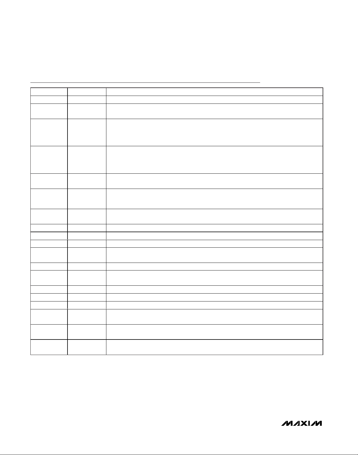
Functional Diagram
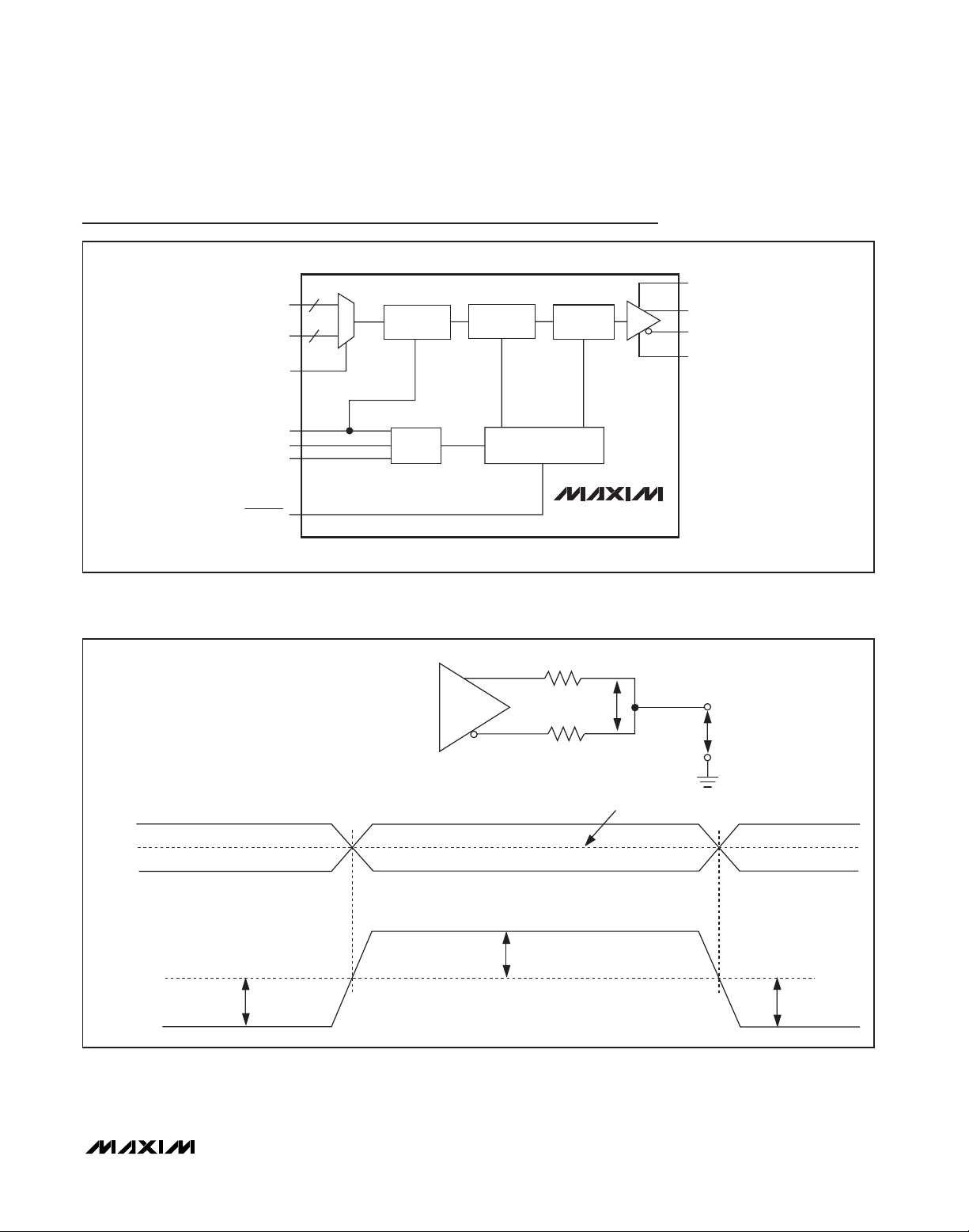
Figure 1. LVDS DC Output Load and Parameters
RGB_IN
CNTL_IN
DE_IN
PCLK_IN
RNG0
RNG1
PWRDWN
PRE
1
INPUT LATCH
0
PLL
DC BALANCE/
ENCODE
TIMING AND CONTROL
PAR-TO-SER
OUT+
OUT-
CMF
MAX9247
/2
R
OUT+
L
OUT-
OUT+
(OUT+) - (OUT-)
(-) VOS(+)
V
OS
V
(-)
OD
OUT-
/2
R
L
((OUT+) + (OUT-))/2
= |VOS(+) - VOS(-)|
∆V
OS
VOD(+)
∆VOD = |VOD(+) - VOD(-)|
V
OD
V
OS
GND
V
(-)
OS
V
= 0V
OD
V
(-)
OD
Page 8

MAX9247
27-Bit, 2.5MHz-to-42MHz
DC-Balanced LVDS Serializer
8 _______________________________________________________________________________________
Figure 2. Parallel Clock Requirements
Figure 3. Output Rise and Fall Times
Figure 4. Synchronous Input Timing
PCLK_IN
t
T
V
V
IHmin
ILmax
t
HIGH
t
F
(OUT+) - (OUT-)
80%
t
R
OUT+
OUT-
C
L
t
RISE
t
LOW
C
R
L
L
80%
20%20%
t
FALL
V
PCLK_IN
RGB_IN[17:0]
CNTL_IN[8:0]
DE_IN
V
V
IHmin
ILmax
V
ILmax
t
SET
IHmin
t
HOLD
V
V
IHmin
ILmax
Page 9

MAX9247
27-Bit, 2.5MHz-to-42MHz
DC-Balanced LVDS Serializer
_______________________________________________________________________________________ 9
Figure 5. Serializer Delay
Figure 6. PLL Lock Time
Figure 7. Power-Down Delay
EXPANDED TIME SCALE
RGB_IN
CNTL_IN
PCLK_IN
OUT_
N
PWRDWN
(OUT+) - (OUT-)
N + 1
HIGH IMPEDANCE
N + 2
V
ILmax
N + 3
N - 1
t
SD
t
LOCK
BIT 0 BIT 19
N
N + 4
V
OD
= 0V
PCLK_IN
PWRDWN
(OUT+) - (OUT-)
PCLK_IN
V
ILmax
t
PD
HIGH IMPEDANCE
Page 10

MAX9247
27-Bit, 2.5MHz-to-42MHz
DC-Balanced LVDS Serializer
10 ______________________________________________________________________________________
Detailed Description
The MAX9247 DC-balanced serializer operates at a
2.5MHz-to-42MHz parallel clock frequency, serializing
18 bits of parallel video data RGB_IN[17:0] when the
data-enable input DE_IN is high, or 9 bits of parallel
control data CNTL_IN[8:0] when DE_IN is low. The
RGB video input data are encoded using 2 overhead
bits, EN0 and EN1, resulting in a serial word length of
20 bits (see Table 1). Control inputs are mapped to 19
bits and encoded with 1 overhead bit, EN0, also resulting in a 20-bit serial word. Encoding reduces EMI and
maintains DC balance across the serial cable. Two
transition words, which contain a unique bit sequence,
are inserted at the transition boundaries of video-tocontrol and control-to-video phases.
Control data inputs C0 to C4 are mapped to 3 bits each
in the serial control word (see Table 2). At the deserializer, 2 or 3 bits at the same state determine the state of
the recovered bit, providing single-bit-error tolerance
for C0 to C4. Control data that may be visible if an error
occurs, such as VSYNC and HSYNC, can be connected to these inputs. Control data inputs C5 to C8 are
mapped to 1 bit each.
Figure 8. Peak-to-Peak Output Offset Voltage
Bit 0 is the LSB and is serialized first. EN[1:0] are encoding bits. S[17:0] are encoded symbols.
Table 1. Serial Video Phase Word Format
Bit 0 is the LSB and is serialized first. C[8:0] are the control inputs.
Table 2. Serial Control Phase Word Format
OUT-
OUT+
((OUT+) + (OUT-))/2
V
OS(P-P)
V
OS(P-P)
012345678910111213141516171819
EN0 EN1 S0 S1 S2 S3 S4 S5 S6 S7 S8 S9 S10 S11 S12 S13 S14 S15 S16 S17
012345678910111213141516171819
E N 0C0C0C0C1C1C1C2C2C2C3C3C3C4C4C4C5C6C7C8
Page 11

MAX9247
27-Bit, 2.5MHz-to-42MHz
DC-Balanced LVDS Serializer
______________________________________________________________________________________ 11
Transition Timing
The transition words require interconnect bandwidth
and displace control data. Therefore, control data is not
sampled (see Figure 9):
• Two clock cycles before DE_IN goes high
• During the video phase
• Two clock cycles after DE_IN goes low
The last sampled control data are latched at the deserializer control data outputs during the transition and video
phases. Video data are latched at the deserializer RGB
data outputs during the transition and control phases.
Applications Information
AC-Coupling Benefits
AC-coupling increases the common-mode voltage to
the voltage rating of the capacitor. Two capacitors are
sufficient for isolation, but four capacitors—two at the
serializer output and two at the deserializer input—provide protection if either end of the cable is shorted to a
high voltage. AC-coupling blocks low-frequency
ground shifts and common-mode noise. The MAX9247
serializer can also be DC-coupled to the MAX9248/
MAX9250 deserializers.
Figures 10 and 12 show an AC-coupled serializer and
deserializer with two capacitors per link. Figures 11 and
13 show the AC-coupled serializer and deserializer with
four capacitors per link.
Selection of AC-Coupling Capacitors
See Figure 14 for calculating the capacitor values for
AC-coupling depending on the parallel clock frequency. The plot shows capacitor values for two- and fourcapacitor-per-link systems. For applications using less
than 18MHz clock frequency, use 0.1µF capacitors.
Frequency-Range Setting RNG[1:0]
The RNG[1:0] inputs select the operating frequency
range of the MAX9247 serializer. An external clock within this range is required for operation. Table 3 shows
the selectable frequency ranges and corresponding
data rates for the MAX9247.
Table 3. Parallel Clock Frequency Range
Select
Figure 9. Transition Timing
PCLK_IN
CNTL_IN
DE_IN
RGB_IN
CONTROL
PHASE
= NOT SAMPLED BY PCLK_IN
TRANSITION
PHASE
VIDEO PHASE
TRANSITION
PHASE
CONTROL
PHASE
RNG1 RNG0
0 0 2.5 to 5 50 to 100
0 1 5 to10 100 to 200
1 0 10 to 20 200 to 400
1 1 20 to 42 400 to 840
PARALLEL
CLOCK (MHz)
SERIAL-DATA RATE
(Mbps)
Page 12

MAX9247
27-Bit, 2.5MHz-to-42MHz
DC-Balanced LVDS Serializer
12 ______________________________________________________________________________________
Figure 10. AC-Coupled MAX9247 Serializer and MAX9250 Deserializer with Two Capacitors per Link
Figure 11. AC-Coupled MAX9247 Serializer and MAX9250 Deserializer with Four Capacitors per Link
V
CC
130Ω
RNG0
RNG1
IN
PLL
TIMING AND
CONTROL
RGB_IN
CNTL_IN
DE_IN
PCLK_IN
RNG0
RNG1
PWRDWN
1
0
INPUT LATCH
PLL
ENCODE
DC BALANCE/
TIMING AND
CONTROL
PAR-TO-SER
OUT
PRE
CMF
130Ω
*
*
82Ω 82Ω
MAX9247
CERAMIC RF SURFACE-MOUNT CAPACITOR
*CAPACITORS CAN BE AT EITHER END.
100Ω DIFFERENTIAL STP CABLE
V
CC
130Ω
IN
RGB_IN
CNTL_IN
DE_IN
PRE
1
0
INPUT LATCH
ENCODE
DC BALANCE/
PAR-TO-SER
OUT
CMF
130Ω
82Ω 82Ω
DECODE
DC BALANCE/
MAX9250
DECODE
DC BALANCE/
1
0
SER-TO-PAR
SER-TO-PAR
R/F
OUTEN
RGB_OUT
CNTL_OUT
DE_OUT
PCLK_OUT
REF_IN
PWRDWN
LOCK
R/F
1
0
OUTEN
RGB_OUT
CNTL_OUT
DE_OUT
PCLK_IN
RNG0
RNG1
PWRDWN
PLL
TIMING AND
CONTROL
MAX9247
CERAMIC RF SURFACE-MOUNT CAPACITOR
RNG0
RNG1
100Ω DIFFERENTIAL STP CABLE
PLL
TIMING AND
CONTROL
MAX9250
PCLK_OUT
REF_IN
PWRDWN
LOCK
Page 13

MAX9247
27-Bit, 2.5MHz-to-42MHz
DC-Balanced LVDS Serializer
______________________________________________________________________________________ 13
Figure 12. AC-Coupled MAX9247 Serializer and MAX9248 Deserializer with Two Capacitors per Link
Figure 13. AC-Coupled MAX9247 Serializer and MAX9248 Deserializer with Four Capacitors per Link
V
CC
130Ω
REFCLK
IN+
IN-
TIMING AND
CONTROL
PLL
DECODE
DC BALANCE/
RGB_IN
CNTL_IN
DE_IN
PCLK_IN
RNG0
RNG1
PWRDWN
PRE
1
0
INPUT LATCH
PLL
ENCODE
DC BALANCE/
TIMING AND
CONTROL
PAR-TO-SER
OUT
CMF
130Ω
*
*
82Ω 82Ω
MAX9247
RNG[0:1]
CERAMIC RF SURFACE-MOUNT CAPACITOR
*CAPACITORS CAN BE AT EITHER END.
100Ω DIFFERENTIAL STP CABLE
V
CC
130Ω
IN+
IN-
DECODE
DC BALANCE/
RGB_IN
CNTL_IN
DE_IN
PRE
1
0
INPUT LATCH
ENCODE
DC BALANCE/
PAR-TO-SER
OUT
CMF
130Ω
82Ω 82Ω
1
0
SER-TO-PAR
SSPLL
1
0
SER-TO-PAR
MAX9248
FIFO
FIFO
R/F
RGB_OUT
CNTL_OUT
DE_OUT
PCLK_OUT
SS
PWRDWN
LOCK
R/F
RGB_OUT
CNTL_OUT
DE_OUT
PCLK_OUT
PCLK_IN
RNG0
RNG1
PWRDWN
PLL
TIMING AND
CONTROL
REFCLK
PLL
TIMING AND
CONTROL
MAX9247
RNG[0:1]
CERAMIC RF SURFACE-MOUNT CAPACITOR
100Ω DIFFERENTIAL STP CABLE
SSPLL
MAX9248
SS
PWRDWN
LOCK
Page 14
MAX9247
27-Bit, 2.5MHz-to-42MHz
DC-Balanced LVDS Serializer
14 ______________________________________________________________________________________
Termination
The MAX9247 has an integrated 100Ω output-termina-
tion resistor. This resistor damps reflections from
induced noise and mismatches between the transmission line impedance and termination resistors at the
deserializer input. With PWRDWN = low or with the supply off, the output termination is switched out and the
LVDS output is high impedance.
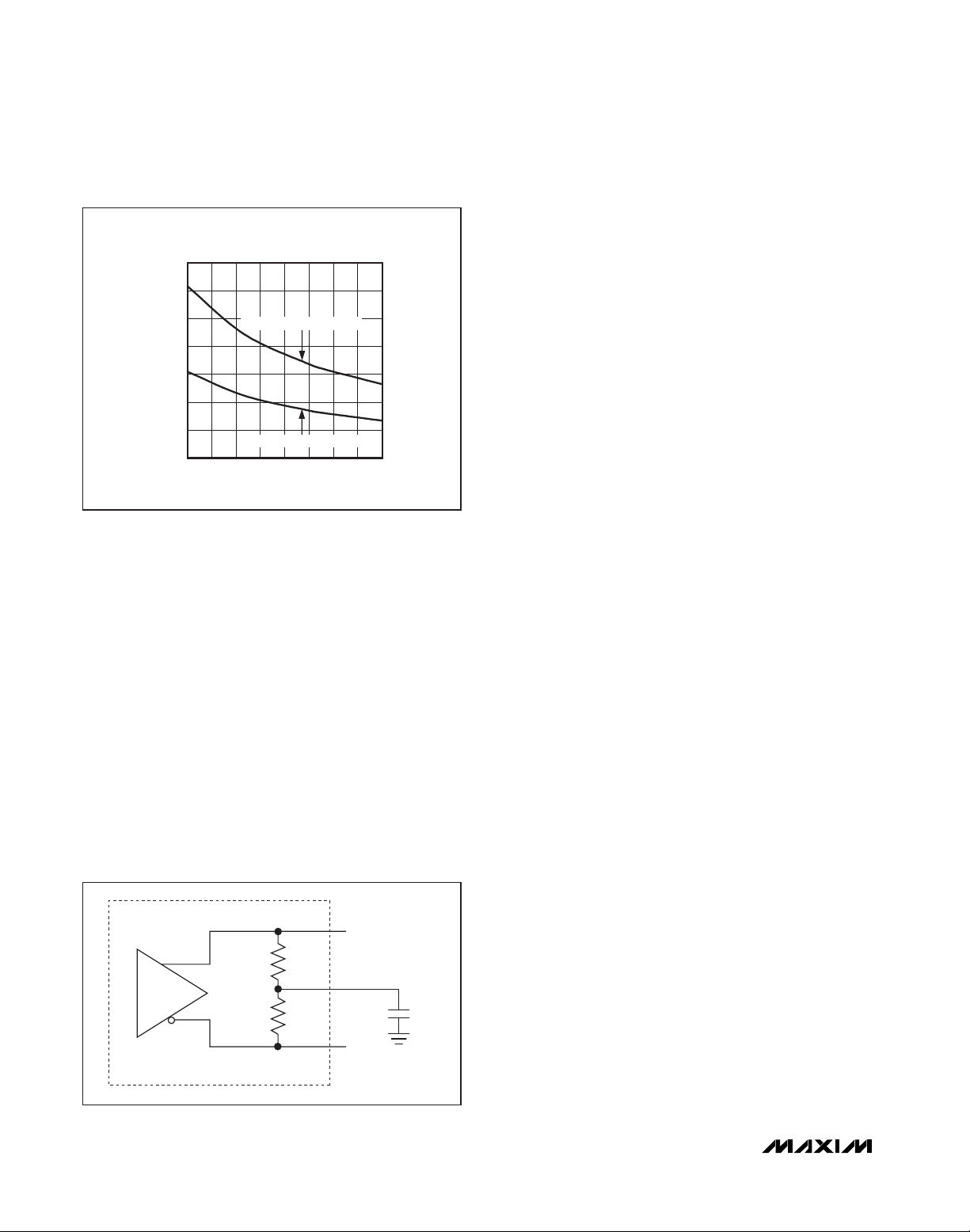
Common-Mode Filter
The integrated 100Ω output termination is made up of
two 50Ω resistors in series. The junction of the resistors
is connected to the CMF pin for connecting an optional
common-mode filter capacitor. Connect the filter
capacitor to ground close to the MAX9247 as shown in
Figure 15. The capacitor shunts common-mode switching current to ground to reduce EMI.
LVDS Output Preemphasis (PRE)
The MAX9247 features a preemphasis mode where extra
current is added to the output and causes the amplitude to increase by 40% to 50% at the transition point.
Preemphasis helps to get a faster transition, better eye
diagram, and improve signal integrity. See the
Typical
Operating Characteristics
. The additional current is
turned on for a short time (360ps, typ) during data transition, and then turned off. Enable preemphasis by driving
PRE high.
Power-Down and Power-Off
Driving PWRDWN low stops the PLL, switches out the
integrated 100Ω output termination, and puts the output
in high impedance to ground and differential. With PWRD-
WN ≤ 0.3V and all LVTTL/LVCMOS inputs ≤ 0.3V or ≥
V
CCIN
- 0.3V, supply current is reduced to 50µA or less.
Driving PWRDWN high starts PLL lock to PCLK_IN and
switches in the 100Ω output termination resistor. The
LVDS output is not driven until the PLL locks. The LVDS
output is high impedance to ground and 100Ω differen-
tial. The 100Ω integrated termination pulls OUT+ and
OUT- together while the PLL is locking so that VOD= 0V.
If V
CC
= 0, the output resistor is switched out and the LVDS
outputs are high impedance to ground and differential.
PLL Lock Time
The PLL lock time is set by an internal counter. The lock
time is 17,100 PCLK_IN cycles. Power and clock should
be stable to meet the lock-time specification.
Input Buffer Supply
The single-ended inputs (RGB_IN[17:0], CNTL_IN[8:0],
DE_IN, RNG0, RNG1, PRE, PCLK_IN, and PWRDWN)
are powered from V
CCIN
. V
CCIN
can be connected to a
1.71V to 3.6V supply, allowing logic inputs with a nominal swing of V
CCIN
. If no power is applied to V
CCIN
when power is applied to VCC, the inputs are disabled
and PWRDWN is internally driven low, putting the
device in the power-down state.
Power-Supply Sequencing of MAX9247
and MAX9248/MAX9250 Video Link
The MAX9247 and MAX9248/MAX9250 video link can
be powered up in several ways. The best approach is
to keep both MAX9247 and MAX9248 powered down
while supplies are ramping up and PCLK_IN of the
MAX9247 and REFCLK of the MAX9248/MAX9250 are
stabilizing. After all of the power supplies of the
MAX9247 and MAX9248/MAX9250 are stable, including
PCLK_IN and REFCLK, do the following:
1) Power up the MAX9247 first
Figure 14. AC-Coupling Capacitor Values vs. Clock Frequency
of 18MHz to 42MHz
Figure 15. Common-Mode Filter Capacitor Connection
AC-COUPLING CAPACITOR VALUE
vs. PARALLEL CLOCK FREQUENCY
140
120
100
80
60
40
CAPACITOR VALUE (nF)
20
0
18 42
FOUR CAPACITORS PER LINK
TWO CAPACITORS PER LINK
21 24 27 33 36 3930
PARALLEL CLOCK FREQUENCY (MHz)
OUT+
/2
R
O
CMF
RO/2
OUT-
C
CMF
Page 15

MAX9247
27-Bit, 2.5MHz-to-42MHz
DC-Balanced LVDS Serializer
______________________________________________________________________________________ 15
2) Wait for at least t
LOCK
of MAX9247 (or 17100 x tT)
to get activity on the link
3) Power up the MAX9248
Power-Supply Circuits and Bypassing
The MAX9247 has isolated on-chip power domains. The
digital core supply (V
CC
) and single-ended input supply
(V
CCIN
) are isolated but have a common ground (GND).
The PLL has separate power and ground (V
CCPLL
and
PLLGND) and the LVDS input also has separate power
and ground (V
CCLVDS
and LVDSGND). The grounds are
isolated by diode connections. Bypass each V
CC
, V
CCIN
,
V
CCPLL
, and V
CCLVDS
pin with high-frequency, surfacemount ceramic 0.1µF and 0.001µF capacitors in parallel
as close to the device as possible, with the smallest value
capacitor closest to the supply pin.
LVDS Output
The LVDS output is a current source. The voltage swing
is proportional to the termination resistance. The output
is rated for a differential load of 100Ω ±1%.
Cables and Connectors
Interconnect for LVDS typically has a differential impedance of 100Ω. Use cables and connectors that have
matched differential impedance to minimize impedance
discontinuities.
Twisted-pair and shielded twisted-pair cables offer
superior signal quality compared to ribbon cable and
tend to generate less EMI due to magnetic field canceling effects. Balanced cables pick up noise as common
mode, which is rejected by the LVDS receiver.
Board Layout
Separate the LVTTL/LVCMOS inputs and LVDS output
to prevent crosstalk. A four-layer PCB with separate layers for power, ground, and signals is recommended.
ESD Protection
The MAX9247 ESD tolerance is rated for IEC 61000-42, Human Body Model, Machine Model, and ISO 10605
standards. IEC 61000-4-2 and ISO 10605 specify ESD
tolerance for electronic systems. The IEC 61000-4-2
discharge components are CS= 150pF and RD=
330Ω (Figure 16). For IEC 61000-4-2, the LVDS outputs
are rated for ±8kV Contact Discharge and ±15kV AirGap Discharge. The Human Body Model discharge
components are CS= 100pF and RD= 1.5kΩ (Figure
17). For the Human Body Model, all pins are rated for
±3kV Contact Discharge. The ISO 10605 discharge
components are CS= 330pF and RD= 2kΩ (Figure
18). For ISO 10605, the LVDS outputs are rated for
±10kV contact and ±30kV air discharge. The Machine
Model discharge components are CS= 200pF and
RD= 0Ω (Figure 19).
Figure 16. IEC 61000-4-2 Contact Discharge ESD Test Circuit
Figure 17. Human Body ESD Test Circuit
Figure 18. ISO 10605 Contact Discharge ESD Test Circuit
Figure 19. Machine Model ESD Test Circuit
R
D
330Ω
HIGH-
VOLTAGE
DC
SOURCE
CHARGE-CURRENT-
LIMIT RESISTOR
150pF
CS
DISCHARGE
RESISTANCE
STORAGE
CAPACITOR
DEVICE
UNDER
TEST
R
D
HIGH-
VOLTAGE
DC
SOURCE
1MΩ
CHARGE-CURRENT-
LIMIT RESISTOR
C
100pF
S
1.5kΩ
DISCHARGE
RESISTANCE
STORAGE
CAPACITOR
DEVICE
UNDER
TEST
R
D
2kΩ
HIGH-
VOLTAGE
DC
SOURCE
CHARGE-CURRENT-
LIMIT RESISTOR
330pF
C
S
DISCHARGE
RESISTANCE
STORAGE
CAPACITOR
DEVICE
UNDER
TEST
R
D
0Ω
HIGH-
VOLTAGE
DC
SOURCE
CHARGE-CURRENT-
LIMIT RESISTOR
200pF
C
S
DISCHARGE
RESISTANCE
STORAGE
CAPACITOR
DEVICE
UNDER
TEST
Page 16

MAX9247
27-Bit, 2.5MHz-to-42MHz
DC-Balanced LVDS Serializer
16 ______________________________________________________________________________________
Chip Information
PROCESS: CMOS
Package Information
For the latest package outline information and land patterns
(footprints), go to www.maxim-ic.com/packages
. Note that a
“+”, “#”, or “-” in the package code indicates RoHS status only.
Package drawings may show a different suffix character, but
the drawing pertains to the package regardless of RoHS status.
PACKAGE
TYPE
PACKAGE
CODE
OUTLINE NO.
LAND
PATTERN NO.
48 LQFP C48+5
21-0054
90-0093
Page 17

MAX9247
27-Bit, 2.5MHz-to-42MHz
DC-Balanced LVDS Serializer
Maxim cannot assume responsibility for use of any circuitry other than circuitry entirely embodied in a Maxim product. No circuit patent licenses are
implied. Maxim reserves the right to change the circuitry and specifications without notice at any time. The parametric values (min and max limits) shown in
the Electrical Characteristics table are guaranteed. Other parametric values quoted in this data sheet are provided for guidance.
17
____________________Maxim Integrated Products, 120 San Gabriel Drive, Sunnyvale, CA 94086 408-737-7600
© 2012 Maxim Integrated Products Maxim is a registered trademark of Maxim Integrated Products, Inc.
Revision History
REVISION
NUMBER
2 5/08
3 4/09
4 4/12 Corrected errors in Absolute Maximum Ratings and Pin Description sections 2, 6
REVISION
DATE
DESCRIPTION
Corrected LQFP package, added +105°C part, changed temperature limits
for +105°C rated part, and added Machine Model ESD text and diagram
Added /V parts in the Ordering Information table and added new Power-
Supply Sequencing of MAX9247 and MAX9248/MAX9250 Video Link section
PAGES
CHANGED
1–6, 15–19
1, 14
 Loading...