

General Description
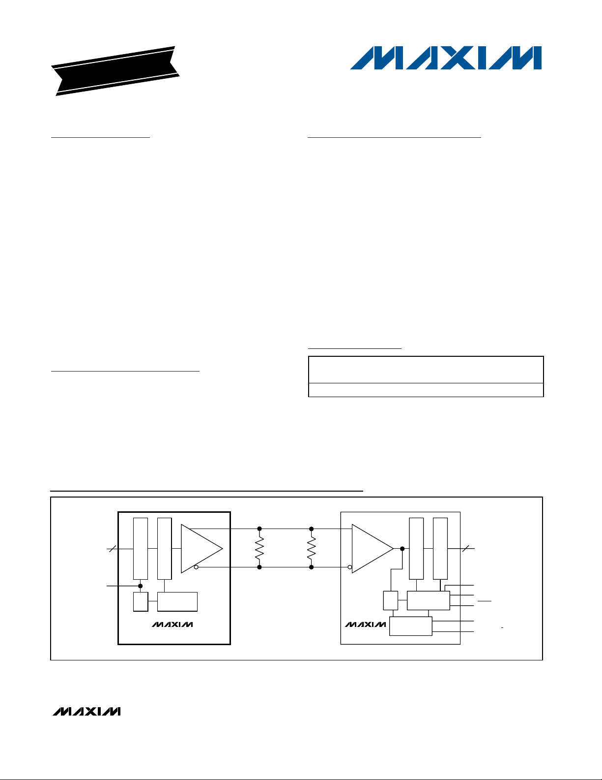
The MAX9235 serializer transforms 10-bit-wide parallel
LVCMOS/LVTTL data into a serial high-speed, low-voltage differential signaling (LVDS) data stream. The serializer typically pairs with deserializers like the
MAX9206, which receives the serial output and transforms it back to 10-bit-wide parallel data.
The MAX9235 transmits serial data at speeds up to
450Mbps over PCB traces or twisted-pair cables. Since
the clock is recovered from the serial data stream,
clock-to-data and data-to-data skew that would be present with a parallel bus are eliminated.
The MAX9235 serializer requires no external components and no control signals and can lock to a 16MHz
to 45MHz system clock. The serializer output is held in
high impedance until the device is fully locked to the
local system clock.
The MAX9235 operates from a single +3.3V supply, is
specified for operation from -40°C to +105°C, and is
available in a 16-pin TQFN (3mm x 3mm) package.
Applications
Features
♦ Stand-Alone Serializer (vs. SERDES) Ideal for
Unidirectional Links
♦ Framing Bits for Deserializer Resync Allow Hot
Insertion Without System Interruption
♦ LVDS Serial Output Rated for Point-to-Point
Applications
♦ Wide Reference Clock Input Range
16MHz to 45MHz
♦ Low 31mA Supply Current
♦ 10-Bit Parallel LVCMOS/LVTTL Interface
♦ Up to 450Mbps Payload Data Rate
♦ Small 16-Pin TQFN (3mm x 3mm) Package
MAX9235
10-Bit LVDS Serializer
________________________________________________________________ Maxim Integrated Products 1
Ordering Information
19-0849; Rev 1; 12/07
For pricing, delivery, and ordering information, please contact Maxim Direct at 1-888-629-4642,
or visit Maxim’s website at www.maxim-ic.com.
EVALUATION KIT
AVAILABLE
Pin Configuration and Functional Diagram appear at end of
data sheet.
Typical Application Circuit
Lane Departures
Security Cameras
Rear View Cameras
Production Line Monitoring
+Denotes a lead-free package.
Note: The device is specified over the -40°C to +105°C temperature range.
*EP = Exposed pad.
PART
M AX 9235E TE + 16 TQFN-EP* 16 to 45 TI633-5
PIN PACKAGE
REF CLOCK
RANGE (MHz)
PKG
CODE
OUT+
IN_
TCLK
10
INPUT LATCH
PARALLEL-TO-SERIAL
TIMING AND
PLL
CONTROL
MAX9235 MAX9206
100Ω 100Ω
OUT-
LVDS
PCB OR
TWISTED PAIR
IN+
10
OUT_
IN-
TIMING AND
PLL
CLOCK
RECOVERY
OUTPUT LATCH
SERIAL-TO-PARALLEL
CONTROL
REFCLK
EN
LOCK
RCLK
RCLK_R/F
MAX9235
10-Bit LVDS Serializer
2 _______________________________________________________________________________________
ABSOLUTE MAXIMUM RATINGS
DC ELECTRICAL CHARACTERISTICS
(VCC= +3.0V to +3.6V, RL= 50Ω ±1%, CL= 10pF, TA= -40°C to +105°C. Typical values are at VCC= +3.3V and TA= +25°C,
unless otherwise noted.) (Notes 1, 2, 3)
Stresses beyond those listed under “Absolute Maximum Ratings” may cause permanent damage to the device. These are stress ratings only, and functional
operation of the device at these or any other conditions beyond those indicated in the operational sections of the specifications is not implied. Exposure to
absolute maximum rating conditions for extended periods may affect device reliability.
VCCto GND.........................................……………-0.3V to +4.0V
IN_, TCLK to GND ......................................-0.3V to (VCC+ 0.3V)
OUT+, OUT- to GND .............................................-0.3V to +4.0V
Output Short-Circuit Duration.....................................Continuous
Continuous Power Dissipation (T
A
= +70°C)
16-Pin TQFN (derate 14.7mW/°C above +70°C) ......1177mW
Storage Temperature Range .............................-65°C to +150°C
Junction Temperature......................................................+150°C
Operating Temperature Range .........................-40°C to +105°C
Lead Temperature (soldering, 10s) .................................+300°C
ESD Protection (Human Body Model, OUT+, OUT-) ...........±8kV
ESD Protection (Human Body Model, IN_, TCLK) ...............±2kV
LVCMOS/LVTLL LOGIC INPUTS (IN0 TO IN9, EN, TCLK)
High-Level Input Voltage V
Low-Level Input Voltage V
Input Current I
LVDS OUTPUTS (OUT+, OUT-)
Differential Output Voltage V
Change in VOD Between
Complementary Output States
Output Offset Voltage V
Change in V
Complementary Output States
Output Short-Circuit Current I
Power-Off Output Current I
POWER SUPPLY
Supply Current I
PARAMETER SYMBOL CONDITIONS MIN TYP MAX UNITS
IH
IL
V
= 0 or V
IN_
Figure 1
Figure 1 1 35 mV
Figure 1
Figure 1 3 35 mV
OUT+ or OUT- = GND,
IN0 to IN9 = EN = V
VCC = 0, V
OUT+
Between
OS
ΔV
ΔV
IN
OD
OD
OS
OS
OS
OX
RL = 100Ω or 50Ω
CC
worst-case pattern
(Figures 2, 4)
2.0 V
GND 0.8 V
CC
or V
R
= 100Ω 600 735 950
L
R
= 50Ω 250 370 470
L
R
= 100Ω 1.025 1.265 1.375
L
R
= 50Ω 1.125 1.265 1.375
L
CC
= 0 or 3.6V -10 +10 µA
OUT-
-20 +20 µA
-13 -15 mA
16MHz 22 35
45MHz 31 45
CC
V
mV
V
mA
MAX9235
10-Bit LVDS Serializer
_______________________________________________________________________________________ 3
AC ELECTRICAL CHARACTERISTICS
(VCC= +3.0V to +3.6V, RL= 50Ω ±1%, CL= 5pF, TA= -40°C to +105°C. Typical values are at VCC= +3.3V and TA= +25°C, unless
otherwise noted.) (Notes 2, 4)
Note 1: Current into a pin is defined as positive. Current out of a pin is defined as negative. All voltages are referenced to ground
except V
OD
, ΔVOD, and VOS.
Note 2: C
L
includes scope probe and test jig capacitance.
Note 3: Parameters 100% tested at T
A
= +25°C. Limits over operating temperature range guaranteed by design and characterization.
Note 4: AC parameters are guaranteed by design and characterization.
TRANSMIT CLOCK (TCLK) TIMING REQUIREMENTS
TCLK Center Frequency f
TCLK Frequency Variation TCFV -200 +200 ppm
TCLK Period t
TCLK Duty Cycle TCDC 40 60 %
TCLK Input Transition Time t
TCLK Input Jitter t
SWITCHING CHARACTERISTICS
Low-to-High Transition Time t
High-to-Low Transition Time t
IN_ Setup to TCLK t
IN_ Hold from TCLK t
PLL Lock Time t
Bus LVDS Bit Width t
Serializer Delay t
PARAMETER SYMBOL CONDITIONS MIN TYP MAX UNITS
TCCF
TCP
CLKT
JIT
LHT
HLT
S
H
PL
BIT
SD
Figure 3 3 6 ns
Figure 4
Figure 4
RL = 100Ω 370 500
R
= 50Ω 350 500
L
RL = 100Ω 370 500
R
= 50Ω 350 500
L
Figure 5 1 ns
Figure 5 3 ns
Figure 6
Figure 7 t
16 45 MHz
22.2 62.5 ns
150
2048 x
t
TCP
/6
TCP
t
TCP
2049 x
t
TCP
/12 ns
( t
/6)
TC P
+ 5
ps
(RMS)
ps
ps
ns
ns

MAX9235
10-Bit LVDS Serializer
4 _______________________________________________________________________________________
Figure 1. Output Voltage Definitions
Figure 2. Worst-Case ICCTest Pattern
Figure 3. Input Clock Transition Time Requirement
Figure 4. Output Load and Transition Times
Figure 5. Data Input Setup and Hold Times
R
OUT+
V
OUT-
L
2
OD
V
R
2
OS
L
TCLK
ODD IN_
EVEN IN_
TCLK
10%
OUT+
OUT-
5pF
R
5pF
V
= (OUT+) - (OUT-)
DIFF
L
90%
t
CLKT
V
DIFF
90%
10%
t
CLKT
80%
20%
t
LHT
t
80%
HLT
3V
0
V
= 0
DIFF
20%
t
TCP
TCLK
IN_
1.5V
1.5V
t
S
t
H
1.5V1.5V
1.5V

MAX9235
10-Bit LVDS Serializer
_______________________________________________________________________________________ 5
Figure 6. PLL Lock Time
Figure 7. Serializer Delay
V
TCLK
OUT±
CC
2.5V 2.5V
IN
IN0–IN9 SYMBOL N
t
SD
t
PL
ACTIVE
IN0–IN9 SYMBOL N + 1
HIGH IMPEDANCEHIGH IMPEDANCE
TCLK
OUT±
1.5V
START BIT
V
OUT0–OUT9 SYMBOL N
= 0 V
DIFF
STOP BIT START BIT STOP BIT
= (OUT+) - (OUT-)
DIFF
OUT0–OUT9 SYMBOL N + 1

MAX9235
10-Bit LVDS Serializer
6 _______________________________________________________________________________________
Typical Operating Characteristics
(VCC= +3.3V, RL= 50Ω, CL = 5pF, TA = +25°C, unless otherwise noted.)
28
31
32
33
30
29
34
3.0 3.33.1 3.2 3.4
3.5
3.6
WORST-CASE PATTERN SUPPLY CURRENT
vs. SUPPLY VOLTAGE
MAX9205 toc01
SUPPLY VOLTAGE (V)
SUPPLY CURRENT (mA)
TCLK = 40MHz
Pin Description
PIN NAME FUNCTION
1–7, 14, 15, 16
8 TCLK
9, 12 GND Ground
10 OUT- Inverting Bus LVDS Differential Output
11 OUT+ Noninverting Bus LVDS Differential Output
13 V
EP EP Exposed Pad. Solder EP to ground for improved heat dissipation.
IN3–IN9, IN0,
IN1, IN2
CC
LVCMOS/LVTTL Data Inputs. Data is loaded into a 10-bit latch by the rising TCLK edge. Each
input is internally pulled to ground.
LVCMOS/LVTTL Reference Clock Input. Accepts a 16MHz to 45MHz clock. TCLK provides a
frequency reference to the PLL and strobes parallel data into the input latch on the rising edge.
Power-Supply Input. Bypass VCC to ground with a 0.1µF capacitor and a 0.001µF capacitor as
close to V
as possible.
CC

MAX9235
10-Bit LVDS Serializer
_______________________________________________________________________________________ 7
Detailed Description
The MAX9235 10-bit serializer transmits data over balanced media that may be a standard twisted-pair cable
or PCB traces at 100Mbps to 450Mbps. The interface
may be single- or double-terminated point-to-point. A
double-terminated point-to-point interface uses a 100Ω-
termination resistor at each end of the interface, resulting in a 50Ω load. The serializer requires a deserializer
such as the MAX9206 for a complete data transmission
application.
A high-state start bit and a low-state stop bit, added
internally, frame the 10-bit parallel input data and
ensure a transition in the serial data stream. Therefore,
12 serial bits are transmitted for each 10-bit parallel
input. The MAX9235 accepts a 16MHz to 45MHz reference clock, producing a serial data rate of 192Mbps
(12 bits x 16MHz) to 540Mbps (12 bits x 45MHz). Since
only 10 bits are from input data, the actual throughput
is 10 times the TCLK frequency.
To transmit data, the serializer sequences through two
modes: initialization mode and data transmission mode.
Initialization Mode
When VCCis applied, the outputs are held in high
impedance and internal circuitry is disabled by on-chip
power-on-reset circuitry. When VCCreaches 2.35V, the
PLL starts to lock to a local reference clock. The reference clock, TCLK, is provided by the system. The serializer locks within 2049 cycles of TCLK. Once locked,
the serializer is ready to send data.
Data Transmission Mode
After initialization, input data at IN0–IN9 are clocked
into the serializer by the TCLK input. Data strobes on
the rising edge of TCLK.
A start bit high and a stop bit low frame the 10-bit data
and function as the embedded clock edge in the serial
data stream. The serial rate is the TCLK frequency
times the data and appended bits. For example, if
TCLK is 40MHz, the serial rate is 40 x 12 (10 + 2 bits) =
480Mbps. Since only 10 bits are from input data, the
payload rate is 40 x 10 = 400Mbps.
High-Impedance State
The serializer output pins (OUT+ and OUT-) are held in
high impedance when VCCis first applied and while the
PLL is locking to the local reference clock. If the serializer goes into high impedance, the deserializer loses
PLL lock and needs to reestablish phase lock before
data transfer can resume. This is done by transmitting
all zeroes for at least one frame.
Applications Information
Power-Supply Bypassing
Bypass VCCwith high-frequency surface-mount ceramic 0.1µF and 0.001µF capacitors in parallel as close to
the device as possible, with the smaller valued capacitor closest to VCC.
Differential Traces and Termination
Use controlled-impedance media and terminate at both
ends of the transmission line in the media's characteristic impedance. Termination with a single resistor at the
end of a point-to-point link typically provides acceptable
performance. The MAX9235 output levels are specified
for double-terminated point-to-point applications. With a
single 100Ω termination, the output swing is larger.
Avoid the use of unbalanced cables such as ribbon or
simple coaxial cable. Balanced cables such as twisted
pair offer superior signal quality and tend to generate
less EMI due to canceling effects. Balanced cables
tend to pick up noise as common mode, which is
rejected by a differential receiver.
Eliminate reflections and ensure that noise couples as
common mode by running the differential traces close
together. Reduce skew by matching the electrical
length of the traces. Excessive skew can result in a
degradation of magnetic field cancellation.
The differential output signals should be routed close to
each other to cancel their external magnetic field.
Maintain a constant distance between the differential
traces to avoid discontinuities in differential impedance.
Avoid 90° turns and minimize the number of vias to further prevent impedance discontinuities.
MAX9235
10-Bit LVDS Serializer
8 _______________________________________________________________________________________
Topologies
The MAX9235 can operate in point-to-point or broadcast topologies.
A point-to-point connection terminated at each end in
the characteristic impedance of the cable or PCB
traces is shown in Figure 8. The total load seen by the
serializer is 50Ω. The double termination typically
reduces reflections compared to a single 100Ω termi-
nation. A single 100Ω termination at the deserializer
input is feasible and will make the differential signal
swing larger.
A point-to-point broadcast configuration is shown in
Figure 9. The low-jitter MAX9150 10-port repeater is
used to reproduce and transmit the serializer output
over 10 double-terminated point-to-point links.
The repeater eliminates nine serializers compared to 10
individual point-to-point serializer-to-deserializer connections. Since repeater jitter subtracts from the serializer-deserializer timing margin, a low-jitter repeater is
essential in most high data rate applications.
Board Layout
For LVDS applications, a four-layer PCB that provides
separate power, ground, and input/output signals is
recommended. Separate LVTTL/LVCMOS and LVDS
signals from each other to prevent coupling into the
LVDS lines.
Figure 8. Double-Terminated Point-to-Point
Figure 9. Point-to-Point Broadcast Using MAX9150 Repeater
PARALLEL
DATA IN
100Ω
SERIALIZED DATA
100Ω
PARALLEL
DATA OUT
MAX9206MAX9235
ASIC
MAX9235
MAX9150
REPEATER
100Ω
100Ω
100Ω
100Ω
ASIC ASIC
MAX9206MAX9206
100Ω
100Ω

MAX9235
10-Bit LVDS Serializer
_______________________________________________________________________________________ 9
Functional Diagram
15
16
14
13
5
6
7
IN5
IN6
8
IN3
OUT-
GND
GND
1
+
3
IN0
4
12 10 9
IN1
IN2
TCLK
IN9
IN8
IN7
MAX9235
IN4 OUT+
2
11
V
CC
THIN QFN
3mm x 3mm
TOP VIEW
Pin Configuration
Chip Information
PROCESS: CMOS
IN_
TCLK
10
INPUT LATCH
PARALLEL-TO-SERIAL
TIMING AND
PLL
CONTROL
OUT+
OUT-
MAX9235

MAX9235
10-Bit LVDS Serializer
10 ______________________________________________________________________________________
Package Information
(The package drawing(s) in this data sheet may not reflect the most current specifications. For the latest package outline information
go to www.maxim-ic.com/packages
.)
MARKING
E/2
D/2
D
AAAA
0.10 C 0.08 C
L
(NE - 1) X e
E2/2
E2
D2/2
D2
b
0.10 M C A B
C
L
L
e
12x16L QFN THIN.EPS
E
(ND - 1) X e
C
L
C
L
A
A2
A1
L
e
k
C
L
e
PACKAGE OUTLINE
8, 12, 16L THIN QFN, 3x3x0.8mm
21-0136
1
I
2

MAX9235
10-Bit LVDS Serializer
______________________________________________________________________________________ 11
Package Information (continued)
(The package drawing(s) in this data sheet may not reflect the most current specifications. For the latest package outline information
go to www.maxim-ic.com/packages
.)
PKG
REF. MIN.
8L 3x3
MIN.
NOM. MAX.
0.70 0.75 0.80
A
b
0.25 0.30 0.35
D
2.90
E
2.90 3.00 3.10
e
L
0.35
ND
NE
0
A1
A2
k
0.25
3.00 3.10
0.65 BSC.
0.55 0.75
0.02
0.20 REF
0.70
0.20
2.90
2.90
0.45
8
2
2
0.05
0
-
-
0.25
NOTES:
1. DIMENSIONING & TOLERANCING CONFORM TO ASME Y14.5M-1994.
2. ALL DIMENSIONS ARE IN MILLIMETERS. ANGLES ARE IN DEGREES.
3. N IS THE TOTAL NUMBER OF T ERMINALS.
4. THE TERMINAL #1 IDENTIFIER AND TERMINAL NUMBERING CONVENTION SHALL CONFORM TO
JESD 95-1 SPP-012. DETAILS OF TERMINAL #1 IDENTIFIER ARE OPTIONAL, BUT MUST BE LOCATED
WITHIN THE ZONE INDICATED. THE TERMINAL #1 IDENTIFIER MAY BE EITHER A MOLD OR
MARKED FEATURE.
5. DIMENSION b APPLIES TO METALLIZED TERMINAL AND IS MEASURED BETWEEN 0.20 mm AND 0.25 mm
FROM TERMINAL TIP.
6. ND AND NE REFER TO THE NUMBER OF TERMINALS ON EACH D AND E SIDE RESPECTIVELY.
7. DEPOPULATION IS POSSIBLE IN A SYMMETRICAL FASHION.
8. COPLANARITY APPLIES TO THE EXPOSED HEAT SINK SLUG AS WELL AS THE TERMINALS .
9. DRAWING CONFORMS TO JEDEC MO220 REVISION C.
10. MARKING IS FOR PACKAGE ORIENTATION REFERENCE ONLY.
11. NUMBER OF LEADS SHOWN ARE FOR REFERENCE ONLY.
12. WARPAGE NOT TO EXCEED 0.10mm.
12L 3x3
NOM. MAX. NOM.
0.75
0.25
3.00
3.00
0.50 BSC.
0.55
12N
3
0.0230.05
0.20 REF
-
MIN. MAX.
0.80
0.70
0.30
0.20
3.10
2.90
3.10
2.90
0.65
0.30
-
0.25
16L 3x3
0.50 BSC.
040.02
0.20 REF
0.75
0.25
3.00
3.00
0.40
16
EXPOSED PAD VARIATIONS
PKG.
0.80
0.30
3.10
3.10
0.50
4
0.05
-
-
CODES
TQ833-1 1.250.25 0.70 0.35 x 45° WEEC1.250.700.25
T1233-1
T1233-3
T1233-4
T1633-2 0. 95
T1633F-3
T1633FH-3 0.65 0.80 0.95
T1633-4 0. 95
T1633-5 0. 95
D2
MIN.
NOM.
MAX.
0.95
0.95
0.65
1.25
1.10
1.25
1.10
1.251.10
1.25
1.10
0.95
0.80
1.10 1.25 0.95 1.10
1.25
1.10
NOM.
MIN.
1.10
0.95
0.95 1.10 0.35 x 45°1.25 WEED-10.95
1.100.95
1.10
0.95
0.80
0.65
0.65 0.80
1.10 1.25
0.95
E2
PACKAGE OUTLINE
8, 12, 16L THIN QFN, 3x3x0.8mm
PIN ID
MAX.
0.35 x 45°
1.25
0.35 x 45°
1.25
0.35 x 45°
0.95
0.225 x 45°
0.95
0.225 x 45°
1.25
0.35 x 45°
0.35 x 45° WEED-2
WEED-1
WEED-11.25
WEED-2
WEED-2
WEED-2
WEED-2
21-0136
JEDEC
2
I
2

MAX9235
10-Bit LVDS Serializer
Maxim cannot assume responsibility for use of any circuitry other than circuitry entirely embodied in a Maxim product. No circuit patent licenses are
implied. Maxim reserves the right to change the circuitry and specifications without notice at any time.
12 ____________________Maxim Integrated Products, 120 San Gabriel Drive, Sunnyvale, CA 94086 408-737-7600
© 2007 Maxim Integrated Products is a registered trademark of Maxim Integrated Products, Inc.
Revision History
REVISION
NUMBER
0 7/07 Initial release —
1 12/07
REVISION DATE REVISION DESCRIPTION
Max clock frequency increased to 45MHz; min value decreased for TCLK
period; changed conditions for Output Short-Circuit and Power-Off Output
Current; various style edits.
PAGES
CHANGED
1, 2, 3, 6, 7
 Loading...