

Page 1
General Description
The MAX9225/MAX9226 serializer/deserializer chipset
reduces wiring by serializing 10 bits onto a single differential pair. Ten bits are serialized in each cycle of the
parallel input clock resulting in a 100Mbps to 200Mbps
net serial-data rate. The MAX9225 serializes the 8-bit
YUV, HSYNC and VSYNC outputs from a camera mounted in the flip part of the phone, reducing wiring through
the hinge to the baseband processor in the base of the
phone. The 2-wire serial interface uses low-current differential signaling (LCDS) for low EMI, high common-mode
noise immunity, and ground-shift tolerance. The
MAX9225/MAX9226 automatically identify the word
boundary in the serial data in case of signal interruption.
The MAX9226 power-down is controlled by the
MAX9225. The MAX9225/MAX9226 consume 3.5µA or
less in power-down mode.
The MAX9225 serializer operates from a single +2.375V
to +3.465V supply and accepts +1.71V to +3.465V
inputs. The MAX9226 deserializer operates from a
+2.375V to +3.465V core supply and has a separate
output buffer supply (V
DDO
), allowing +1.71V to
+3.465V output high levels.
The MAX9225/MAX9226 are specified over the -40°C to
+85°C extended temperature range and are available
in 16-pin TQFN (3mm x 3mm x 0.8mm) packages with
an exposed paddle.
Applications
Cell Phone Cameras
Digital Cameras
Features
♦ Ideal for Serializing Cell Phone Camera Parallel
Interface
♦ MAX9225 Serializes 8-Bit YUV, HSYNC, and VSYNC
♦ LCDS Rejects Common-Mode Noise
♦ Automatic Location of Word Boundary After
Signal Interruption
♦ Power-Down Control Through the Serial Link
♦ Power-Down Supply Current
0.5µA (max) for MAX9225
3.0µA (max) for MAX9226
♦ +2.375V to +3.465V Core Supply Voltage
♦ Parallel I/O Interfaces Directly to 1.8V to 3.3V Logic
♦ ±15kV Human Body Model ESD Protection
♦ -40°C to +85°C Operating Temperature Range
MAX9225/MAX9226
10-Bit, Low-Power, 10MHz-to-20MHz
Serializer and Deserializer Chipset
________________________________________________________________
Maxim Integrated Products
1
Ordering Information
19-3680; Rev 1; 12/07
For pricing, delivery, and ordering information, please contact Maxim Direct at 1-888-629-4642,
or visit Maxim’s website at www.maxim-ic.com.
EVALUATION KIT
AVAILABLE
+
Denotes lead-free package.
*
EP = Exposed paddle.
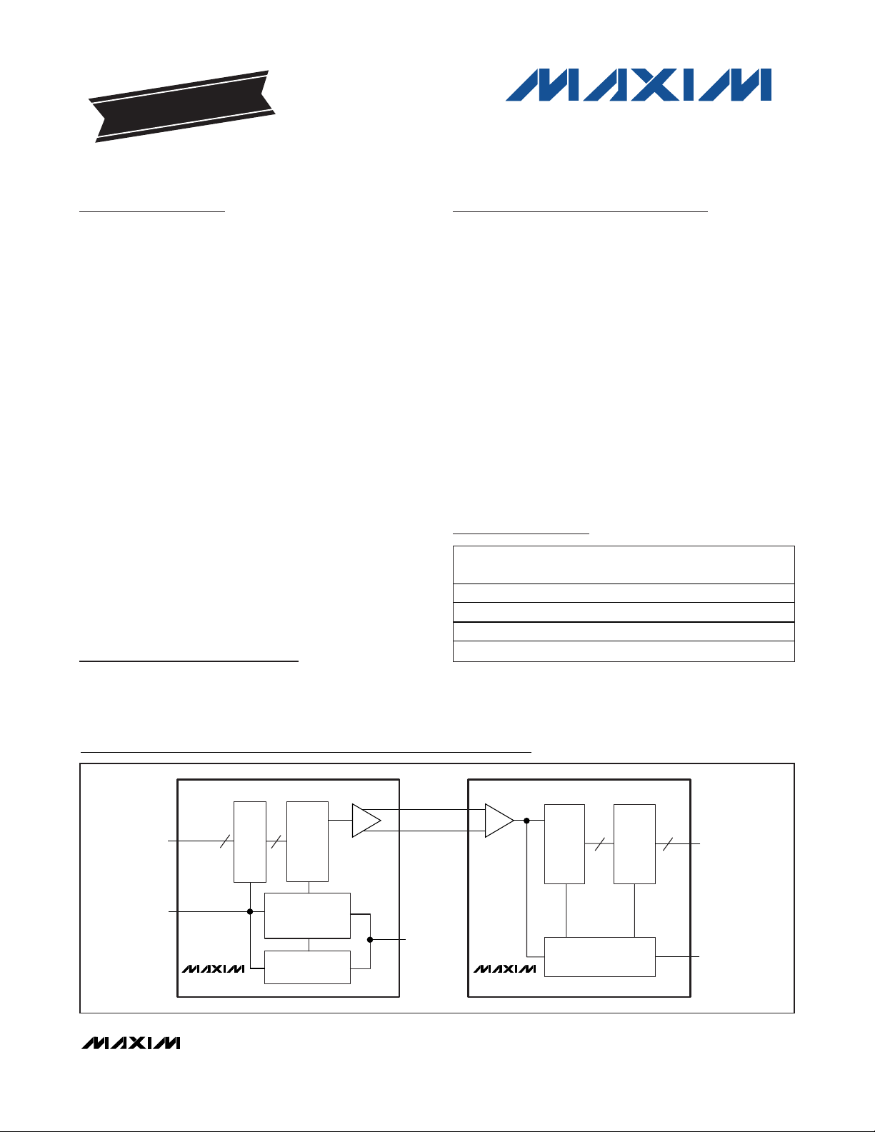
Typical Application Circuit
Pin Configurations appear at end of data sheet.
PA R T
M A X9 2 2 5 E TE - 40°C to + 85° C 16 TQ FN - E P * T1633- 4AD O
M AX 9225E TE + - 40°C to + 85° C 16 TQ FN - E P * T1633- 4AD O
M A X9 2 2 6 E TE - 40°C to + 85° C 16 TQ FN - E P * T1633- 4AD X
M AX 9226E TE + - 40°C to + 85° C 16 TQ FN - E P * T1633- 4AD X
T EM P
R A N G E
PIN -
PA C K A G E
PK G
C O D E
T O P
M A R K
PARALLEL
DATA IN
PIXEL
CLOCK IN
INPUT
LATCH
MAX9225 MAX9226
PARALLEL
TO
SERIAL
TIMING
AND
CONTROL
DLL
LCDS
POWER-DOWN
CONTROL
SERIAL
TO
PARALLEL
TIMING AND CONTROL
OUTPUT
LATCH
PARALLEL
DATA OUT
PIXEL
CLOCK OUT
Page 2
MAX9225/MAX9226
10-Bit, Low-Power, 10MHz-to-20MHz
Serializer and Deserializer Chipset
2 _______________________________________________________________________________________
ABSOLUTE MAXIMUM RATINGS
DC ELECTRICAL CHARACTERISTICS (MAX9225)
(VDD= +2.375V to +3.465V, TA= -40°C to +85°C, unless otherwise noted. Typical values are at VDD= +2.5V, TA= +25°C.) (Notes 1, 2)
Stresses beyond those listed under “Absolute Maximum Ratings” may cause permanent damage to the device. These are stress ratings only, and functional
operation of the device at these or any other conditions beyond those indicated in the operational sections of the specifications is not implied. Exposure to
absolute maximum rating conditions for extended periods may affect device reliability.
VDDto GND...........................................................-0.5V to +4.0V
V
DDO
to GND.........................................................-0.5V to +4.0V
Serial Interface (SDO+, SDO-, SDI+,
SDI-) to GND .....................................................-0.5V to +4.0V
Single-Ended Inputs (DIN_, PCLKIN,
PWRDN) to GND ....................................-0.5V to (V
DD
+ 0.5V)
Single-Ended Outputs (DOUT_,
PCLKOUT) to GND ..............................-0.5V to (V
DDO
+ 0.5V)
Continuous Power Dissipation (T
A
= +70°C)
16-Pin TQFN (3mm x 3mm x 0.8mm)
Multilayer PCB (derate 20.8mW/°C
above +70°C).............................................................1667mW
Single-Layer PCB (derate 15.6mW/°C
above +70°C).............................................................1250mW
Storage Temperature Range .............................-65°C to +150°C
Junction Temperature......................................................+150°C
Lead Temperature (soldering, 10s) .................................+300°C
ESD Protection (Human Body Model)
SDO+, SDO-, SDI+, SDI- to GND ...............................> ±15kV
All Other Pins to GND ...................................................> ±2kV
SINGLE-ENDED INPUTS (PCLKIN, DIN_, PWRDN)
High-Level Input Voltage V
Low-Level Input Voltage V
LCDS OUTPUT (SDO+, SDO-)
Differential Output Current
Output Short-Circuit Current I
POWER SUPPLY
Supply Current I
Worst-Case Pattern Supply Current I
Power-Down Supply Current I
PARAMETER SYMBOL CONDITIONS MIN TYP MAX UNITS
IN
I
ODH
I
ODL
OS
DD
DDW
DDZ
IH
IL
VIN = 0V to V
-0.3V ≤ VIN < 0VInput Current I
VDD < VIN ≤ (VDD + 0.3V)
High level 575 643 880
Low level 200 229 300
Shorted to 0V or V
VDD = 2.5V
VDD = 2.5V,
Figure 1
All inputs = low 0.5 µA
DD
DD
PCLKIN = 10MHz,
100Mbps
PCLKIN = 20MHz,
200Mbps
PCLKIN = 10MHz,
100Mbps
PCLKIN = 20MHz,
200Mbps
1.19 V
-0.3 +0.3 V
-20 +20
-100 +100
4.7 8.2
6.2 8.2
4.7 10.6
6.2 10.6
+ 0.3 V
DD
880 µA
µA
µA
mA
mA
Page 3
MAX9225/MAX9226
10-Bit, Low-Power, 10MHz-to-20MHz
Serializer and Deserializer Chipset
_______________________________________________________________________________________ 3
DC ELECTRICAL CHARACTERISTICS (MAX9226)
(VDD= +2.375V to +3.465V, V
DDO
= +1.71V to +3.465V, TA= -40°C to +85°C, unless otherwise noted. Typical values are at VDD=
V
DDO
= +2.5V, TA= +25°C.) (Notes 1, 2)
SINGLE-ENDED OUTPUTS (PCLKOUT, DOUT_)
High-Level Output Voltage V
Low-Level Output Voltage V
Output Short-Circuit Current I
LCDS INPUT (SDI+, SDI-)
Differential Input-Current Threshold I
Common-Mode Input Current I
Differential Input Impedance Z
Common-Mode Input Impedance Z
Input Capacitance C
POWER SUPPLY
Supply Current I
Worst-Case Pattern
Supply Current
Power-Down Supply Current I
Supply Difference V
GROUND POTENTIAL
Ground Difference V
PARAMETER SYMBOL CONDITIONS MIN TYP MAX UNITS
V
OH
OL
OS
ID
IC
TOT
I
TOTW
TOTZ
SD
GD
ID
IC
IN
= +2.375V to +3.465V, IOH = -1mA 0.8 x V
DDO
V
= +2.375V to +3.465V, IOL = 1mA 0.2 V
DDO
Output shorted
to ground
IIC = 0µA, VDD = 3.3V ±5% 69 90 114
IIC = 0µA, VDD = 2.8V ±5% 82 108 137
IIC = 0µA, VDD = 2.5V ±5% 95 125 161
IIC = ±300µA, VDD = 3.3V ±5% 67 91 117
IIC = ±300µA, VDD = 2.8V ±5% 86 108 141
IIC = ±300µA 90 167 375 Ω
SDI+ or SDI- to ground 2 pF
VDD = V
(Note 4)
CL = 5pF, VDD =
V
DDO
Figure 2 (Note 4)
(Note 4) 0.3 3.0 µA
MAX9225 VDD to MAX9226 V
MAX9225 to MAX9226 ground difference -0.2 +0.2 V
DDO
= 2.5V,
= 2.5V
DDO
V
= 2.375V -2
DDO
V
= 3.135V -9
DDO
V
= 3.465V -25
DDO
-300 ±400 +300 µA
PCLKOUT = 10MHz,
100Mbps
PCLKOUT = 20MHz,
200Mbps
PCLKOUT = 10MHz,
100Mbps
PCLKOUT = 20MHz,
200Mbps
DD
-5 +5 %
V
mA
400 µA
Ω
8.4 12
mA
9.1 12
9.7 12
mA
11.6 13
Page 4
MAX9225/MAX9226
10-Bit, Low-Power, 10MHz-to-20MHz
Serializer and Deserializer Chipset
4 _______________________________________________________________________________________
AC ELECTRICAL CHARACTERISTICS (MAX9225)
(VDD= +2.375V to +3.465V, TA= -40°C to +85°C, unless otherwise noted. Typical values are at VDD= +2.5V, TA= +25°C.) (Note 3)
AC ELECTRICAL CHARACTERISTICS (MAX9226)
(VDD= V
DDO
= +2.375V to +3.465V, CL= 5pF, TA= -40°C to +85°C, unless otherwise noted. Typical values are at VDD= V
DDO
=
+2.5V, T
A
= +25°C.) (Notes 3, 5)
Note 1: Current into a pin is defined as positive. Current out of a pin is defined as negative. All voltages are referenced to ground.
Note 2: Maximum and minimum limits over temperature are guaranteed by design and characterization. Devices are production
tested at T
A
= +85°C.
Note 3: Parameters are guaranteed by design and characterization and are not production tested. Limits are set at ±6 sigma.
Note 4: I
TOT
= IDD+ I
DDO
.
Note 5: C
L
includes probe and test jig capacitance.
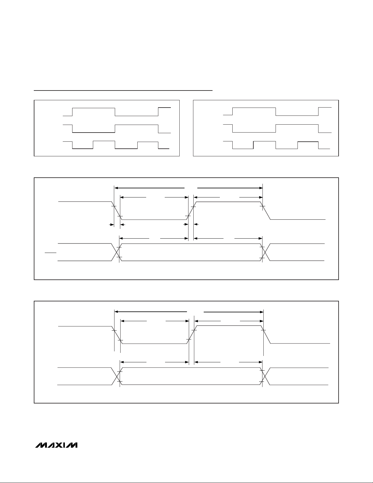
PCLKIN INPUT REQUIREMENTS (Figure 3)
Input Rise Time t
Input Fall Time t
PCLKIN Period t
High-Level Pulse Width t
Low-Level Pulse Width t
Setup Time t
Hold Time t
PCLKOUT Period t
High-Level Pulse Width t
Low-Level Pulse Width t
Data Valid Before PCLKOUT t
Data Valid After PCLKOUT t
SERIALIZER AND DESERIALIZER LINK
Power-Up Time
Power-Down Time t
PARAMETER SYMBOL CONDITIONS MIN TYP MAX UNITS
R
F
P
PWH
PWL
S
H
PARAMETER SYMBOL CONDITIONS MIN TYP MAX UNITS
Figure 4 50 100 ns
P
PWH
PWL
t
PU1
t
PU2
PWRDN
Figure 4 0.4 x t
Figure 4 0.4 x t
Figure 4 5 ns
VB
Figure 4 5 ns
VA
From V
are ramping up
From PWRDN low to high
From PWRDN high to low 2.8 10 µs
DD
= V
= 2.375V when supplies
DDO
50 100 ns
0.3 x t
P
0.3 x t
P
3ns
1ns
P
P
2ns
2ns
0.7 x t
0.7 x t
0.6 x t
0.6 x t
11,264 x
t
P
4096 x
t
ns
P
ns
P
ns
P
ns
P
ns
P
Page 5
MAX9225/MAX9226
10-Bit, Low-Power, 10MHz-to-20MHz
Serializer and Deserializer Chipset
_______________________________________________________________________________________ 5
Test Circuits/Timing Diagrams
Figure 3. Serializer Input Timing
Figure 1. Serializer Worst-Case Switching Pattern
Figure 2. Deserializer Worst-Case Switching Pattern
Figure 4. Deserializer Output Timing
ODD DIN_
EVEN DIN_
PCLKIN
t
PWL
V
PCLKIN
DIN_
PWRDN
VIH IS THE MINIMUM HIGH-LEVEL INPUT, AND VIL IS THE MAXIMUM LOW-LEVEL INPUT (SEE THE
IH
V
IL
t
F
t
S
V
IH
V
IL
ODD DOUT_
EVEN DOUT_
PCLKOUT
t
P
t
PWH
V
IH
V
IL
t
R
DC ELECTRICAL CHARACTERISTICS
t
H
TABLE)
V
IH
V
IH
V
IL
V
OH
PCLKOUT
DOUT_
V
IS THE MINIMUM HIGH-LEVEL OUTPUT, AND VOL IS THE MAXIMUM LOW-LEVEL OUTPUT (SEE THE
OH
t
P
t
t
PWH
VA
V
OH
V
OH
V
OL
TABLE)
t
PWL
V
OH
V
OL
t
VB
V
OH
V
OL
V
OL
DC ELECTRICAL CHARACTERISTICS
Page 6

MAX9225/MAX9226
10-Bit, Low-Power, 10MHz-to-20MHz
Serializer and Deserializer Chipset
6 _______________________________________________________________________________________
Typical Operating Characteristics
(VDD= V
DDO
= +2.8V, logic input levels = 0 to +2.8V, logic output load CL= 5pF, TA= +25°C, unless otherwise noted.)
MAX9225
SUPPLY CURRENT vs. SUPPLY VOLTAGE
MAX9225 toc01
SUPPLY VOLTAGE (V)
SUPPLY CURRENT (mA)
3.33.12.92.72.5
4
6
8
10
2
2.3 3.5
DIN[9:0] = ALL LOW
PCLKIN = 20MHz
PCLKIN = 10MHz
MAX9225
SUPPLY CURRENT vs. SUPPLY VOLTAGE
MAX9225 toc02
SUPPLY VOLTAGE (V)
SUPPLY CURRENT (mA)
3.33.12.92.72.5
4
6
8
10
2
2.3 3.5
DIN[9:0] = ALL HIGH
PCLKIN = 20MHz
PCLKIN = 10MHz
MAX9225
SUPPLY CURRENT vs. SUPPLY VOLTAGE
MAX9225 toc03
SUPPLY VOLTAGE (V)
SUPPLY CURRENT (mA)
3.33.12.92.72.5
4
6
8
10
2
2.3 3.5
DIN[9:0] = WORST-CASE SWITCHING PATTERN
PCLKIN = 20MHz
PCLKIN = 10MHz
MAX9225
SUPPLY CURRENT vs. FREQUENCY
MAX9225 toc04
FREQUENCY (MHz)
SUPPLY CURRENT (mA)
18161412
4
6
8
10
2
10 20
DIN[9:0] = ALL LOW
VDD = 3.3V
VDD = 2.8V
VDD = 2.5V
MAX9225
SUPPLY CURRENT vs. FREQUENCY
MAX9225 toc05
FREQUENCY (MHz)
SUPPLY CURRENT (mA)
18161412
4
6
8
10
2
10 20
DIN[9:0] = ALL HIGH
VDD = 3.3V
VDD = 2.8V
VDD = 2.5V
MAX9225
SUPPLY CURRENT vs. FREQUENCY
MAX9225 toc06
FREQUENCY (MHz)
SUPPLY CURRENT (mA)
18161412
4
6
8
10
2
10 20
DIN[9:0] = WORST-CASE SWITCHING PATTERN
VDD = 3.3V
VDD = 2.8V
VDD = 2.5V
MAX9225 POWER-DOWN
SUPPLY CURRENT vs. FREQUENCY
MAX9225 toc07
SUPPLY VOLTAGE (MHz)
SUPPLY CURRENT (μA)
3.1 3.32.92.72.5
0.08
0.04
0.12
0.16
0.20
0
2.3 3.5
PCLKIN = LOW
PWRDN = LOW
DIN[9:0] = ALL LOW
MAX9226
SUPPLY CURRENT vs. SUPPLY VOLTAGE
MAX9226 toc08
SUPPLY VOLTAGE (V)
SUPPLY CURRENT (mA)
3.33.12.92.72.5
8
9
10
11
7
2.3 3.5
DIN[9:0] = ALL LOW
PCLKOUT = 20MHz
PCLKOUT = 10MHz
MAX9226
SUPPLY CURRENT vs. SUPPLY VOLTAGE
MAX9226 toc09
SUPPLY VOLTAGE (V)
SUPPLY CURRENT (mA)
3.33.12.92.72.5
8
9
10
11
7
2.3 3.5
DIN[9:0] = ALL HIGH
PCLKOUT = 20MHz
PCLKOUT = 10MHz
Page 7

MAX9225/MAX9226
10-Bit, Low-Power, 10MHz-to-20MHz
Serializer and Deserializer Chipset
_______________________________________________________________________________________ 7
Typical Operating Characteristics (continued)
(VDD= V
DDO
= +2.8V, logic input levels = 0 to +2.8V, logic output load CL= 5pF, TA= +25°C, unless otherwise noted.)
MAX9226
SUPPLY CURRENT vs. FREQUENCY
MAX9226 toc13
FREQUENCY (MHz)
SUPPLY CURRENT (mA)
18161412
8
9
10
11
7
10 20
DIN[9:0] = WORST-CASE SWITCHING PATTERN
VDD = 3.3V
VDD = 2.8V
VDD = 2.5V
MAX9226 POWER-DOWN
SUPPLY CURRENT vs. FREQUENCY
MAX9226 toc14
SUPPLY VOLTAGE (V)
SUPPLY CURRENT (μA)
3.1 3.32.92.72.5
0.3
0.4
0.5
0.6
0.2
2.3 3.5
SDI+/SDI- PULLED UP TO V
DD
DOUT[9:0] = ALL LOW
MAX9226 DOUT OUTPUT-HIGH VOLTAGE
vs. SOURCE CURRENT
MAX9226 toc15
SOURCE CURRENT (mA)
DOUT (V)
0.80.60.40.2
2.00
1.75
1.50
2.25
2.50
2.75
1.25
0 1.0
V
DDO
= 2.375V
V
DDO
= 2V
V
DDO
= 1.71V
SUPPLY CURRENT vs. SUPPLY VOLTAGE
11
DIN[9:0] = WORST-CASE SWITCHING PATTERN
10
9
SUPPLY CURRENT (mA)
8
7
2.3 3.5
MAX9226
PCLKOUT = 20MHz
PCLKOUT = 10MHz
SUPPLY VOLTAGE (V)
MAX9226
SUPPLY CURRENT vs. FREQUENCY
11
DIN[9:0] = ALL LOW
MAX9226 toc10
3.33.12.92.72.5
10
9
SUPPLY CURRENT (mA)
8
7
10 20
VDD = 3.3V
VDD = 2.8V
VDD = 2.5V
FREQUENCY (MHz)
18161412
MAX9226 toc11
SUPPLY CURRENT vs. FREQUENCY
11
DIN[9:0] = ALL HIGH
10
9
SUPPLY CURRENT (mA)
8
7
10 20
MAX9226
VDD = 3.3V
VDD = 2.8V
FREQUENCY (MHz)
MAX9226 toc12
VDD = 2.5V
18161412
MAX9226 DOUT OUTPUT-LOW VOLTAGE
vs. SINK CURRENT
150
V
= +1.71V TO +2.375V
DDO
120
90
DOUT (mV)
60
30
0
0 1.0
SINK CURRENT (mA)
MAX9226 toc16
INPUT IMPEDANCE (Ω)
0.80.60.40.2
MAX9226 DIFFERENTIAL INPUT
IMPEDANCE vs. SUPPLY VOLTAGE
160
140
120
100
80
2.3 3.5
SUPPLY VOLTAGE (V)
3.1 3.32.92.72.5
MAX9226 toc17
Page 8
MAX9225/MAX9226
10-Bit, Low-Power, 10MHz-to-20MHz
Serializer and Deserializer Chipset
8 _______________________________________________________________________________________
Pin Description (MAX9225)
Pin Description (MAX9226)
PIN NAME FUNCTION
1–7,
14, 15, 16
8 PCLKIN
9 PWRDN
10 SDO- Inverting LCDS Serial-Data Output
11 SDO+ Noninverting LCDS Serial-Data Output
12 GND Ground
13 V
— EP Exposed Paddle. Connect EP to ground.
DIN6–DIN0,
DIN9, DIN8, DIN7
DD
Single-Ended Parallel Data Inputs. The 10 data bits are loaded into the input latch on the rising
edge of PCLKIN. 1.71V to 3.465V tolerant. Internally pulled down to GND.
Parallel Clock Input. The rising edge of PCLKIN (typically the pixel clock) latches the parallel
data input. Internally pulled down to GND.
Power-Down Input. Pull PWRDN low to place the MAX9225/MAX9226 in power-down mode.
Drive PWRDN high for normal operation. Internally pulled down to GND.
Core Supply Voltage. Bypass to GND with 0.1µF and 0.01µF capacitors in parallel as close to
the device as possible with the smallest value capacitor closest to the supply pin.
PIN NAME FUNCTION
1 GND Ground
2 SDI+ Noninverting LCDS Serial-Data Input
3 SDI- Inverting LCDS Serial-Data Input
4V
5 PCLKOUT
6–15 DOUT0–DOUT9 Single-Ended Parallel Data Output. DOUT[9:0] are valid on the rising edge of PCLKOUT.
16 V
— EP Exposed Paddle. Connect EP to ground.
DD
DDO
Core Supply Voltage. Bypass to GND with 0.1µF and 0.01µF capacitors in parallel as close to
the device as possible, with the smallest value capacitor closest to the supply pin.
Parallel Clock Output. Parallel output data are valid on the rising edge of PCLKOUT (typically
the pixel clock).
Output Supply Voltage. Bypass to GND with 0.1µF and 0.01µF capacitors in parallel as close to
the device as possible with the smallest value capacitor closest to the supply pin.
Page 9

MAX9225/MAX9226
10-Bit, Low-Power, 10MHz-to-20MHz
Serializer and Deserializer Chipset
_______________________________________________________________________________________ 9
Functional Diagram (MAX9225)
Functional Diagram (MAX9226)
Detailed Description
The MAX9225 serializer operates at a 10MHz-to-20MHz
parallel clock frequency, serializing 10 bits of parallel
input data DIN[9:0] in each cycle of the parallel clock.
DIN[9:0] are latched on the rising edge of PCLKIN. The
data and internally generated serial clock are combined and transmitted through SDO+/SDO- using multilevel LCDS. The MAX9226 deserializer receives the
LCDS signal on SDI+/SDI-. The deserialized data and
recovered parallel clock are available at DOUT[9:0]
and PCLKOUT. Output data is valid on the rising edge
of PCLKOUT.
Bit 0 (DIN[0]) is transmitted first. Boundary bits OH1
and OH2 are used by the MAX9226 deserializer to
identify the word boundary. OH1 is the inverse polarity
of data bit 9 (DIN[9]), and OH2 is the inverse polarity of
OH1. Therefore, at least two level transitions are guaranteed in one word. The clock is recovered from the
serial input.
LCDS
The MAX9225/MAX9226 use a proprietary multilevel
LCDS interface. Figure 5 provides a representation of
the data and clock in the multilevel LCDS interface. This
interface offers advantages over other chipsets, such
as requiring only one differential pair as the transmission medium, the inherently aligned data and clock,
and much smaller current levels than the 4mA typically
found in traditional LVDS interfaces.
MAX9225/MAX9226 Handshaking
The handshaking function of the MAX9225/MAX9226
provides bidirectional communication between the two
devices in case a word boundary error is detected. Prior
to data transmission, the MAX9225 serializer adds
boundary bits (OH) to the end of the latched word.
These boundary bits are the inverse of the last bit of the
latched word. During data transmission, the MAX9226
deserializer continuously monitors the state of the
boundary bits of each word. If a word boundary error is
detected, the serial link is pulled up to V
DD
and the
MAX9226 powers down. The MAX9225 detects the
pullup of the serial link and powers down for 1.0µs. After
1.0µs, the MAX9225 powers up, causing the power-up
of the MAX9226. Then the word boundary is reestablished, and data transfer resumes. The handshaking
function is disabled when PWRDN is pulled low.
Serial word format:
SDO+
DIN[9:0]
PCLKIN
MAX9225
INPUT
LATCH
PARALLEL
TO
SERIAL
TIMING
AND
CONTROL
DLL
SDO-
PWRDN
0123456789OH1OH2
SDI+
SDI-
MAX9226
SERIAL
TO
PARALLEL
TIMING AND CONTROL
OUTPUT
LATCH
DOUT[9:0]
PCLKOUT
Page 10
MAX9225/MAX9226
Applications Information
PCLKIN Latch Edge
The parallel data input of the MAX9225 serializer is
latched on the rising edge of PCLKIN. Figure 3 shows
the serializer input timing.
PCLKOUT Strobe
The serial-data output of the MAX9226 deserializer is
valid on the rising edge of PCLKOUT. Figure 4 shows
the deserializer output timing.
Power-Down and Power-Up
Driving PWRDN low puts the MAX9225 in power-down
mode and sends a pulse to power down the MAX9226.
In power-down mode, the DLL is stopped, SDO+/SDOare high impedance to ground and differential, and the
LCDS link is weakly biased around (V
DD
- 0.8V). With
PWRDN and all inputs low, the combined MAX9225/
MAX9226 supply current is reduced to 3.5µA or less.
Driving PWRDN high starts DLL lock to PCLKIN and initiates a MAX9226 power-up sequence. The MAX9225
LCDS output is not driven until the DLL locks. 11,264
clock cycles are required for the power-up and link synchronization before valid DIN can be latched. See
Figure 6 for an overall power-up and power-down timing diagram. For normal operation, PCLKIN must be
running and settled before driving PWRDN high.
If V
DD
= 0, the LCDS outputs are high impedance to
ground and differential.
Ground-Shift Tolerance
The MAX9225/MAX9226 are designed to function normally in the event of a slight shift in ground potential.
However, the MAX9226 deserializer ground must be
within ±0.2V relative to the MAX9225 serializer ground
to maintain proper operation.
MAX9226 Output Buffer Supply (V
DDO
)
The MAX9226 parallel outputs are powered from V
DDO
,
which accepts a +1.71V to +3.465V supply, allowing
direct interface to inputs with 1.8V to 3.3V logic levels.
10-Bit, Low-Power, 10MHz-to-20MHz
Serializer and Deserializer Chipset
10 ______________________________________________________________________________________
Figure 5. Multilevel LCDS Output Representation
PARALLEL DATA INPUT
PCLK IN
DIN[9:0]
DIN
EXAMPLE
INPUT
LCDS SERIAL-DATA OUTPUT FOR EXAMPLE INPUT (SD0+/SDO-)
01234567 89
11010010 11
NOTE: OH1 AND OH2 ARE OPPOSITE POLARITY.
0
0
OH1
OH211 111100
Page 11

Flex Cable, PCB Interconnect,
and Connectors
Interconnect for LCDS typically has a differential impedance of 100Ω. Use interconnect and connectors that have
matched differential impedance to minimize impedance
discontinuities.
Board Layout and Supply Bypassing
Separate the LVTTL/LVCMOS and LCDS signals to prevent crosstalk. A PCB or flex with separate layers for
power, ground, and signals is recommended.
Bypass each VDDand V
DDO
pin with high-frequency,
surface-mount ceramic 0.1µF and 0.01µF capacitors in
parallel as close to the device as possible, with the
smallest value capacitor closest to the supply pin.
ESD Protection
The MAX9225/MAX9226 are rated for ±15kV ESD
protection using the Human Body Model. The Human
Body Model discharge components are CS= 100pF and
RD= 1.5kΩ (Figure 7).
Chip Information
PROCESS: CMOS
MAX9225/MAX9226
10-Bit, Low-Power, 10MHz-to-20MHz
Serializer and Deserializer Chipset
______________________________________________________________________________________ 11
Figure 6. MAX9225/MAX9226 Power-Up/Power-Down Sequence
Figure 7. Human Body Model ESD Test Circuit
POWER-UP AND LINK
SYNCHRONIZATION
12
DON'T CARE
t
PU2
1
LOW
HIGH
PWRDN
PCLKIN
DIN_
DOUT_
PCLKOUT
IN POWERDOWN
DATA TRANSFER
1
POWERDOWN
t
PWRDN
N
N
DON'T CARE
IN POWERDOWN
LOW
HIGH
R
D
1.5kΩ
DISCHARGE
RESISTANCE
C
S
STORAGE
CAPACITOR
HIGH-
VOLTAGE
DC
SOURCE
1MΩ
CHARGE-CURRENT-
LIMIT RESISTOR
100pF
DEVICE
UNDER
TEST
Page 12
MAX9225/MAX9226
10-Bit, Low-Power, 10MHz-to-20MHz
Serializer and Deserializer Chipset
12 ______________________________________________________________________________________
Pin Configurations
TOP VIEW
11
MAX9225
2
DIN5 SDO+
SDO-
DIN4
V
DIN9
DIN8
DIN7
GND
12 10 9
13
DD
14
15
16
13
DIN6
TQFN-EP
PWRDN
4
DIN3
DOUT3
11
MAX9226
2
SDI+ DOUT5
DOUT4
SDI-
DOUT2
8
DOUT1
7
DOUT0
6
PCLKOUT
5
4
DD
V
DOUT6
12 10 9
PCLKIN
8
DIN0
7
DIN1
6
DIN2
5
DOUT7
DOUT8
DOUT9
V
DDO
13
14
15
16
13
GND
TQFN-EP
Page 13
MAX9225/MAX9226
10-Bit, Low-Power, 10MHz-to-20MHz
Serializer and Deserializer Chipset
______________________________________________________________________________________ 13
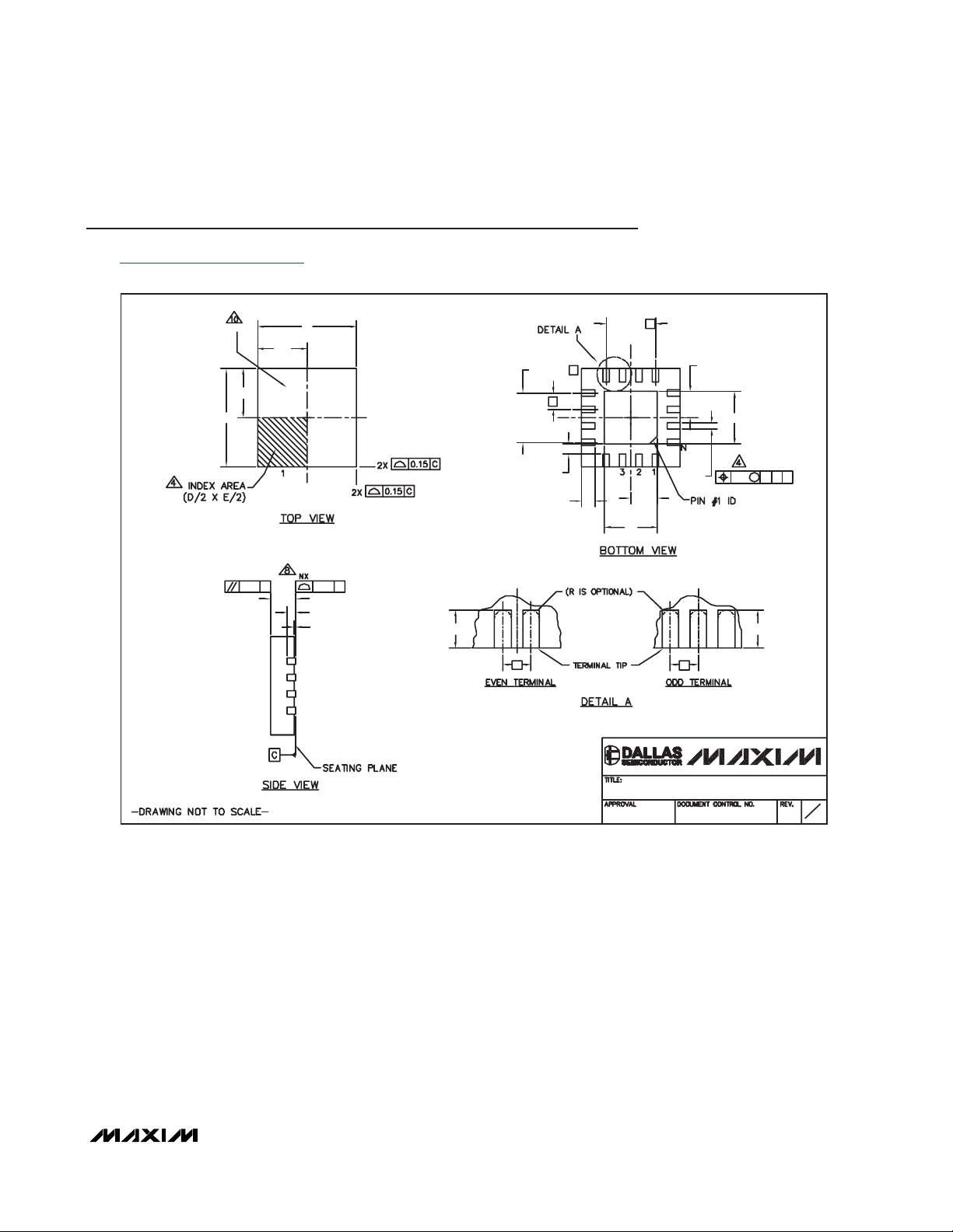
Package Information
(The package drawing(s) in this data sheet may not reflect the most current specifications. For the latest package outline information,
go to www.maxim-ic.com/packages
.)
E/2
AAAA
L
(NE - 1) X e
E2/2
E2
D2/2
D2
b
0.10 M C A B
C
L
L
e
12x16L QFN THIN.EPS
E
(ND - 1) X e
C
L
C
L
A
A2
A1
L
e
k
C
L
e
MARKING
D/2
D
0.10 C 0.08 C
PACKAGE OUTLINE
8, 12, 16L THIN QFN, 3x3x0.8mm
21-0136
1
I
2
Page 14

MAX9225/MAX9226
10-Bit, Low-Power, 10MHz-to-20MHz
Serializer and Deserializer Chipset
14 ______________________________________________________________________________________
Package Information (continued)
(The package drawing(s) in this data sheet may not reflect the most current specifications. For the latest package outline information,
go to www.maxim-ic.com/packages
.)
PKG
REF. MIN.
MIN.
0.70 0.75 0.80
A
b
0.25 0.30 0.35
D
2.90
E
2.90 3.00 3.10
e
L
0.35
ND
NE
A1
A2
k
0.25
0.65 BSC.
0
0.20 REF
8L 3x3
NOM. MAX.
3.00 3.10
0.55 0.75
8
2
2
0.02
-
0.05
12L 3x3
NOM. MAX. NOM.
0.70
0.75
0.20
0.25
2.90
3.00
2.90
3.00
0.50 BSC.
0.45
0.55
0
0.20 REF
-
0.25
0.80
0.30
3.10
3.10
0.65
12N
3
0.0230.05
-
MIN. MAX.
0.70
0.20
2.90
2.90
0.30
040.02
-
0.25
16L 3x3
0.75
0.25
3.00
3.00
0.50 BSC.
0.40
16
4
0.20 REF
-
NOTES:
1. DIMENSIONING & TOLERANCING CONFORM TO ASME Y14.5M-1994 .
2. ALL DIMENSIONS ARE IN MILLIMETERS. ANGLES ARE IN DEGREES.
3. N IS THE TOTAL NUMBER OF TERMINALS.
4. THE TERMINAL #1 IDENTIFIER AND TERMINAL NUMBERING CONVENTION SHALL CONFORM TO
JESD 95-1 SPP-012. DETAILS OF TERMINAL #1 IDENTIFIER ARE OPTIONAL, BUT MUST BE LOCATED
WITHIN THE ZONE INDICATED. THE TERMINAL #1 IDENTIFIER MAY BE EITHER A MOLD OR
MARKED FEATURE.
5. DIMENSION b APPLIES TO METALLIZED TERMINAL AND IS MEASURED BETWEEN 0.20 mm AND 0.25 mm
FROM TERMINAL TIP.
6. ND AND NE REFER TO THE NUMBER OF TERMINALS ON EACH D AND E SIDE RESPECTIVELY.
7. DEPOPULATION IS POSSIBLE IN A SYMMETRICAL FASHION.
8. COPLANARITY APPLIES TO THE EXPOSED HEAT SINK SLUG AS WELL AS THE TERMINALS .
9. DRAWING CONFORMS TO JEDEC MO220 REVISION C.
10. MARKING IS FOR PACKAGE ORIENTATION REFERENCE ONLY.
11. NUMBER OF LEADS SHOWN ARE FOR REFERENCE ONLY.
12. WARPAGE NOT TO EXCEED 0.10mm.
0.80
0.30
3.10
3.10
0.50
0.05
EXPOSED PAD VARIATIONS
PKG.
CODES
TQ833-1 1.250.25 0.70 0.35 x 45° WEEC1.250.700.25
T1233-1
T1233-3
T1233-4
T1633-2 0.95
T1633F-3
T1633FH-3 0.65 0.80 0.95
T1633-4 0.95
T1633-5 0.95
-
D2
MIN.
NOM.
MAX.
0.95
0.95
0.65
1.25
1.10
1.25
1.10
1.251.10
1.25
1.10
0.95
0.80
1.10 1.25 0.95 1.10
1.25
1.10
E2
NOM.
MIN.
0.95
0.95 1.10 0.35 x 45°1.25 WEED-10.95
0.95
0.65
0.65 0.80
0.95
MAX.
1.10
1.25
1.100.95
1.10
1.25
0.80
0.95
0.95
1.25
1.10 1.25
PACKAGE OUTLINE
8, 12, 16L THIN QFN, 3x3x0.8mm
PIN ID
0.35 x 45°
0.35 x 45°
0.35 x 45°
0.225 x 45°
0.225 x 45°
0.35 x 45°
0.35 x 45° WEED-2
JEDEC
WEED-1
WEED-11.25
WEED-2
WEED-2
WEED-2
WEED-2
21-0136
2
I
2
Page 15

MAX9225/MAX9226
10-Bit, Low-Power, 10MHz-to-20MHz
Serializer and Deserializer Chipset
Maxim cannot assume responsibility for use of any circuitry other than circuitry entirely embodied in a Maxim product. No circuit patent licenses are
implied. Maxim reserves the right to change the circuitry and specifications without notice at any time.
Maxim Integrated Products, 120 San Gabriel Drive, Sunnyvale, CA 94086 408-737-7600 ____________________
15
© 2007 Maxim Integrated Products is a registered trademark of Maxim Integrated Products, Inc.
Springer
Revision History
REVISION
NUMBER
0 1/06 Initial release —
1 12/07
REVISION
DATE
DESCRIPTION
Changed max output short-circuit current from -20 to -25 in EC table; various
style changes.
PAGES
CHANGED
2, 3, 11
 Loading...