

Page 1
For pricing, delivery, and ordering information, please contact Maxim Direct at 1-888-629-4642,
or visit Maxim’s website at www.maxim-ic.com.
General Description
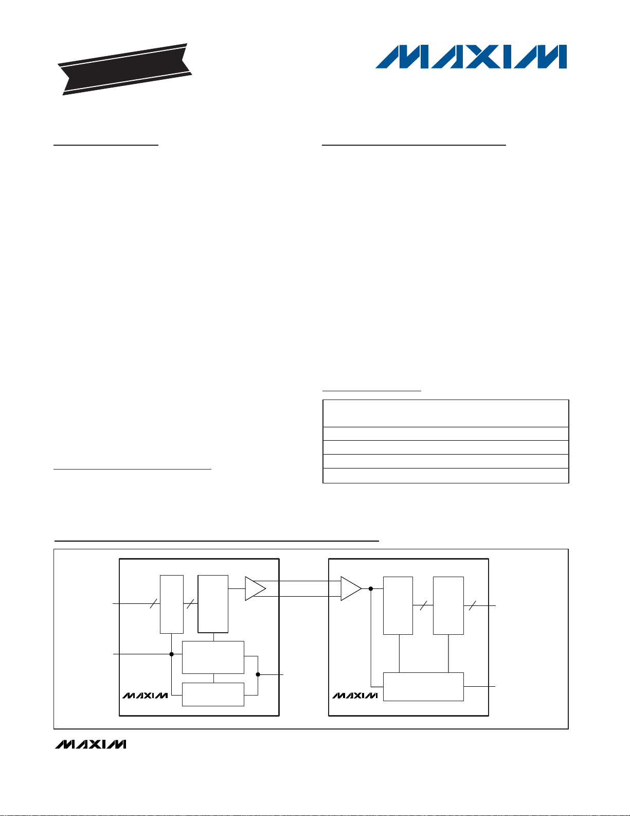
The MAX9223/MAX9224 serializer/deserializer chipsets
reduce wiring by serializing 22 bits onto a single differential pair. 22 bits are serialized in each cycle of the parallel input clock resulting in a 110Mbps to 220Mbps net
serial-data rate ideal for cell phone QVGA and QCIF displays. The MAX9223 serializes the 18-bit RGB, VSYNC,
HSYNC, and two control signals from the baseband
processor to reduce wiring through the hinge to the LCD
controller. The 2-wire serial interface uses low-current differential signaling (LCDS) for low EMI, high commonmode noise immunity, and ground-shift tolerance. The
MAX9223/MAX9224 automatically identify the word
boundary in serial data in case of signal interruption. The
MAX9224 power-down is controlled by the MAX9223.
The MAX9223 and MAX9224 consume 3.5µA or less in
power-down mode.
The MAX9223 serializer operates from a single +2.375V
to +3.465V supply and accepts +1.71V to +3.465V
inputs. The MAX9224 deserializer operates from a
+2.375V to +3.465V core supply and has a separate
output buffer supply (V
DDO
), allowing +1.71V to
+3.465V output high levels.
The MAX9223/MAX9224 are specified over the -40°C to
+85°C extended temperature range and are available
in 28-pin TQFN (4mm x 4mm x 0.8mm) packages with
an exposed paddle.
Applications
Cell Phones
LCDs
Digital Cameras
Features
♦ Ideal for Serializing Cell Phone LCD or Imager
Parallel Interface
♦ MAX9223 Serializes 18-Bit RGB, VSYNC, HSYNC,
and Two Control Signals
♦ LCDS Rejects Common-Mode Noise
♦ Automatic Location of Word Boundary After Signal
Interruption
♦ Power-Down Control Through the Serial Link
♦ Power-Down Supply Current
0.5µA (max)—MAX9223
3.0µA (max)—MAX9224
♦ +2.375V to +3.465V Core Supply Voltage
♦ Parallel I/O Interfaces Directly to 1.8V to 3.3V Logic
♦ ±15kV Human Body Model ESD Protection
♦ -40°C to +85°C Operating Temperature Range
MAX9223/MAX9224
22-Bit, Low-Power, 5MHz to 10MHz
Serializer and Deserializer Chipsets
________________________________________________________________ Maxim Integrated Products 1
Ordering Information
19-3861; Rev 1; 12/07
PART
TEMP RANGE
PINPACKAGE
PKG
CODE
MAX9223ETI
T2844-1
MAX9223ETI+
T2844-1
MAX9224ETI
T2844-1
MAX9224ETI+
T2844-1
EVALUATION KIT
AVAILABLE
+Denotes lead-free package.
*EP = Exposed paddle.
Typical Application Circuit
TIMING
AND
CONTROL
PARALLEL
TO
SERIAL
PARALLEL
DATA OUT
TIMING AND CONTROL
OUTPUT
LATCH
PIXEL
CLOCK OUT
DLL
LCDS
POWER-DOWN
CONTROL
SERIAL
TO
PARALLEL
PARALLEL
DATA IN
PIXEL
CLOCK IN
LATCH
INPUT
MAX9223 MAX9224
Pin Configurations appear at end of data sheet.
-40°C to +85°C 28 TQFN-EP*
-40°C to +85°C 28 TQFN-EP*
-40°C to +85°C 28 TQFN-EP*
-40°C to +85°C 28 TQFN-EP*
Page 2
MAX9223/MAX9224
22-Bit, Low-Power, 5MHz to 10MHz
Serializer and Deserializer Chipset
2 _______________________________________________________________________________________
ABSOLUTE MAXIMUM RATINGS
DC ELECTRICAL CHARACTERISTICS—MAX9223
(VDD= +2.375V to +3.465V, TA= -40°C to +85°C, unless otherwise noted. Typical values are at VDD= +2.5V, TA= +25°C.) (Notes 1, 2)
Stresses beyond those listed under “Absolute Maximum Ratings” may cause permanent damage to the device. These are stress ratings only, and functional
operation of the device at these or any other conditions beyond those indicated in the operational sections of the specifications is not implied. Exposure to
absolute maximum rating conditions for extended periods may affect device reliability.
VDDto GND...........................................................-0.5V to +4.0V
V
DDO
to GND.........................................................-0.5V to +4.0V
Serial Interface (SDO+, SDO-, SDI+,
SDI-) to GND .....................................................-0.5V to +4.0V
Single-Ended Inputs (DIN_, PCLKIN,
PWRDN) to GND ....................................-0.5V to (VDD+ 0.5V)
Single-Ended Outputs (DOUT_,
PCLKOUT) to GND ..............................-0.5V to (V
DDO
+ 0.5V)
Continuous Power Dissipation (T
A
= +70°C)
28-Pin TQFN (4mm x 4mm x 0.8mm)
Multilayer PCB (derate 28.6mW/°C
above +70°C).............................................................2286mW
Single-Layer PCB (derate 20.8mW/°C
above +70°C).............................................................1667mW
Storage Temperature Range .............................-65°C to +150°C
Junction Temperature......................................................+150°C
Lead Temperature (soldering, 10s) .................................+300°C
ESD Protection (Human Body Model)
SDO+, SDO-, SDI+, SDI- to GND ...............................> ±15kV
All Other Pins ................................................................> ±2kV
PARAMETER
SYMBOL
CONDITIONS
MIN
TYP
MAX
UNITS
SINGLE-ENDED INPUTS (PCLKIN, DIN_, PWRDN)
High-Level Input Voltage V
IH
V
Low-Level Input Voltage V
IL
-0.3
V
VIN = 0V to V
DD
-20 +20
-0.3V ≤ VIN < 0VInput Current I
IN
VDD < VIN ≤ (VDD + 0.3V)
µA
LCDS OUTPUT (SDO+, SDO-)
I
ODH
High level 600 643 880
Differential Output Current (Note 3)
I
ODL
Low level 200 229 300
µA
Output Short-Circuit Current I
OS
Shorted to 0V or V
DD
880 µA
POWER SUPPLY
PCLKIN = 5MHz
(110Mbps)
4.4 8.2
Supply Current I
DD
VDD = 2.5V,
DIN_ = all low or
all high
PCLKIN = 10MHz
(220Mbps)
5.6 8.2
mA
PCLKIN = 5MHz
(110Mbps)
4.1
Worst-Case Pattern Supply Current
I
DDW
VDD = 2.5V,
Figure 1
PCLKIN = 10MHz
(220Mbps)
5.4
mA
Power-Down Supply Current I
DDZ
All inputs = low 0.5 µA
1.19 V
-100 +100
DD
+ 0.3
+0.3
10.6
10.6
Page 3

MAX9223/MAX9224
22-Bit, Low-Power, 5MHz to 10MHz
Serializer and Deserializer Chipset
_______________________________________________________________________________________ 3
DC ELECTRICAL CHARACTERISTICS—MAX9224
(VDD= +2.375V to +3.465V, V
DDO
= +1.71V to +3.465V, TA= -40°C to +85°C, unless otherwise noted. Typical values are at VDD=
V
DDO
= +2.5V, TA= +25°C.) (Notes 1, 2)
PARAMETER
SYMBOL
CONDITIONS
MIN
TYP
MAX
UNITS
SINGLE-ENDED OUTPUTS (PCLKOUT, DOUT_)
High-Level Output Voltage V
OH
V
DDO
= +2.375V to +3.465V, IOH = -1mA
V
Low-Level Output Voltage V
OL
V
DDO
= +2.375V to +3.465V, IOL = 1mA 0.2 V
V
DDO
= 2.375V -2
V
DDO
= 3.135V -9
Output Short-Circuit Current I
OS
Output shorted
to ground
V
DDO
= 3.465V -25
mA
LCDS INPUT (SDI+, SDI-)
Differential Input-Current Threshold
I
ID
400 µA
Common-Mode Input Current I
IC
µA
IIC = 0µA at VDD = 3.3V ±5% 69 90 109
IIC = 0µA at VDD = 2.8V ±5% 82 108 132
IIC = 0µA at VDD = 2.5V ±5% 95 125 153
IIC = ±300µA at VDD = 3.3V ±5% 67 91 112
Differential Input Impedance Z
ID
IIC = ±300µA at VDD = 2.8V ±5% 86 108 136
Ω
Common-Mode Input Impedance Z
IC
IIC = ±300µA 90 167 375 Ω
Input Capacitance C
IN
SDI+ or SDI- to ground 2 pF
POWER SUPPLY
PCLKOUT = 5MHz
(110Mbps)
912
Supply Current (Note 4) I
TOT
VDD = V
DDO
= 2.5V
DOUT_ = all high or
all low
PCLKOUT = 10MHz
(220Mbps)
912
mA
PCLKOUT = 5MHz
(110Mbps)
10 12
Worst-Case Pattern
Supply Current (Note 4)
CL = 5pF, VDD =
V
DDO
= 2.5V,
Figure 2
PCLKOUT = 10MHz
(220Mbps)
10 12
mA
Power-Down Supply Current
(Note 4)
I
TOTZ
3µA
Supply Difference V
SD
MAX9223 VDD to MAX9224 V
DD
-5 +5 %
GROUND POTENTIAL
Ground Difference V
GD
MAX9223 to MAX9224 ground difference -0.2
V
0.8 x V
DDO
-300 ±500 +300
I
TOTW
0.08
+0.2
Page 4
MAX9223/MAX9224
22-Bit, Low-Power, 5MHz to 10MHz
Serializer and Deserializer Chipset
4 _______________________________________________________________________________________
AC ELECTRICAL CHARACTERISTICS—MAX9223
(VDD= +2.375V to +3.465V, TA= -40°C to +85°C, unless otherwise noted. Typical values are at VDD= +2.5V, TA= +25°C.) (Note 3)
PARAMETER
SYMBOL
CONDITIONS
MIN
TYP
MAX
UNITS
PCLKIN INPUT REQUIREMENTS (Figure 3)
Input Rise Time t
R
2ns
Input Fall Time t
F
2ns
PCLKIN Period t
P
100 200 ns
High-Level Pulse Width t
PWH
ns
Low-Level Pulse Width t
PWL
ns
Setup Time t
S
3ns
Hold Time t
H
1ns
AC ELECTRICAL CHARACTERISTICS—MAX9224
(VDD= V
DDO
= +2.375V to +3.465V, CL= 5pF, TA= -40°C to +85°C, unless otherwise noted. Typical values are at VDD= V
DDO
=
+2.5V, T
A
= +25°C.) (Notes 3, 5)
PARAMETER
SYMBOL
CONDITIONS
MIN
TYP
MAX
UNITS
PCLKOUT Period t
P
Figure 4 100 200 ns
High-Level Pulse Width t
PWH
Figure 4
ns
Low-Level Pulse Width t
PWL
Figure 4
ns
Data Valid Before PCLKOUT t
VB
Figure 4 5 ns
Data Valid After PCLKOUT t
VA
Figure 4 5 ns
SERIALIZER AND DESERIALIZER LINK
t
PU1
From V
DD
= V
DDO
= 2.375V when supplies
are ramping up
t
P
Power-Up Time
t
PU2
From PWRDN low to high
t
P
ns
Power-Down Time
From PWRDN high to low 2.8 10 µs
Note 1: Current into a pin is defined as positive. Current out of a pin is defined as negative. All voltages are referenced to ground.
Note 2: Maximum and minimum limits over temperature are guaranteed by design and characterization. Devices are production
tested at T
A
= +85°C.
Note 3: Parameters are guaranteed by design and characterization, and are not production tested. Limits are set at ±6 sigma.
Note 4: I
TOT
= IDD+ I
DDO
.
Note 5: C
L
includes probe and test jig capacitance.
t
PWRDN
0.3 x t
0.3 x t
0.4 x t
0.4 x t
P
P
P
P
0.7 x t
0.7 x t
0.6 x t
0.6 x t
6144 x
4096 x
P
P
P
P
Page 5
MAX9223/MAX9224
22-Bit, Low-Power, 5MHz to 10MHz
Serializer and Deserializer Chipset
_______________________________________________________________________________________ 5
Test Circuits/Timing Diagrams
t
S
V
IL
V
IH
t
R
V
IH
t
PWL
t
P
t
H
V
IL
V
IH
PCLKIN
t
PWH
V
IL
V
IH
V
IL
V
IH
DIN_
PWRDN
t
F
VIH IS THE MINIMUM HIGH-LEVEL INPUT AND VIL IS THE MAXIMUM LOW-LEVEL INPUT (SEE THE
DC ELECTRICAL CHARACTERISTICS
TABLE).
Figure 3. Serializer Input Timing
ODD DIN_
EVEN DIN_
PCLKIN
Figure 1. Serializer Worst-Case Switching Pattern
ODD DOUT_
EVEN DOUT_
PCLKOUT
Figure 2. Deserializer Worst-Case Switching Pattern
t
VB
V
OL
V
OH
V
OH
t
PWL
t
P
t
VA
V
OL
V
OH
PCLKOUT
t
PWH
V
OL
V
OH
V
OL
V
OH
DOUT_
V
OH
IS THE MINIMUM HIGH-LEVEL OUTPUT AND VOL IS THE MAXIMUM LOW-LEVEL OUTPUT (SEE THE
DC ELECTRICAL CHARACTERISTICS
TABLE).
Figure 4. Deserializer Output Timing
Page 6

MAX9223/MAX9224
22-Bit, Low-Power, 5MHz to 10MHz
Serializer and Deserializer Chipset
6 _______________________________________________________________________________________
Typical Operating Characteristics
(VDD= V
DDO
= +2.8V, logic input levels = 0 to +2.8V, logic output load CL= 5pF, TA= +25°C, unless otherwise noted.)
10
8
6
4
2
2.3 2.92.5 2.7 3.1 3.3 3.5
MAX9223
SUPPLY CURRENT vs. SUPPLY VOLTAGE
MAX9233/4 toc01
SUPPLY VOLTAGE (V)
SUPPLY CURRENT (mA)
PCLKIN = 10MHz
PCLKIN = 5MHz
DIN[21:0] = ALL LOW
10
8
6
4
2
2.3 2.92.5 2.7 3.1 3.3 3.5
MAX9223
SUPPLY CURRENT vs. SUPPLY VOLTAGE
MAX9233/4 toc02
SUPPLY VOLTAGE (V)
SUPPLY CURRENT (mA)
PCLKIN = 10MHz
PCLKIN = 5MHz
DIN[21:0] = ALL HIGH
10
8
6
4
2
2.3 2.92.5 2.7 3.1 3.3 3.5
MAX9223
SUPPLY CURRENT vs. SUPPLY VOLTAGE
MAX9233/4 toc03
SUPPLY VOLTAGE (V)
SUPPLY CURRENT (mA)
PCLKIN = 10MHz
PCLKIN = 5MHz
DIN[21:0] = WORST-CASE SWITCHING PATTERN
10
8
6
4
2
5678910
MAX9223
SUPPLY CURRENT vs. FREQUENCY
MAX9233/4 toc04
FREQUENCY (MHz)
SUPPLY CURRENT (mA)
VDD = 3.3V
VDD = 2.8V
VDD = 2.5V
DIN[21:0] = ALL LOW
8
6
4
2
5678910
MAX9223
SUPPLY CURRENT vs. FREQUENCY
MAX9233/4 toc05
FREQUENCY (MHz)
SUPPLY CURRENT (mA)
VDD = 3.3V
VDD = 2.8V
VDD = 2.5V
DIN[21:0] = ALL HIGH
8
6
4
2
5678910
MAX9223
SUPPLY CURRENT vs. FREQUENCY
MAX9233/4 toc06
FREQUENCY (MHz)
SUPPLY CURRENT (mA)
VDD = 3.3V
VDD = 2.8V
VDD = 2.5V
DIN[21:0] = WORST-CASE SWITCHING PATTERN
0.20
0.16
0.12
0.08
0.04
0
2.3 2.92.5 2.7 3.1 3.3 3.5
MAX9223 POWER-DOWN
SUPPLY CURRENT vs. SUPPLY VOLTAGE
MAX9233/4 toc07
SUPPLY VOLTAGE (V)
SUPPLY CURRENT (μA)
PCLKIN = LOW
PWRDN = LOW
DIN[21:0] = ALL LOW
12
11
10
9
8
7
2.3 2.92.5 2.7 3.1 3.3 3.5
MAX9224
SUPPLY CURRENT vs. SUPPLY VOLTAGE
MAX9233/4 toc08
SUPPLY VOLTAGE (V)
SUPPLY CURRENT (mA)
PCLKOUT = 10MHz
PCLKOUT = 5MHz
DOUT[21:0] = ALL LOW
12
11
10
9
8
7
2.3 2.92.5 2.7 3.1 3.3 3.5
MAX9224
SUPPLY CURRENT vs. SUPPLY VOLTAGE
MAX9233/4 toc09
SUPPLY VOLTAGE (V)
SUPPLY CURRENT (mA)
PCLKOUT = 10MHz
PCLKOUT = 5MHz
DOUT[21:0] = ALL HIGH
Page 7

MAX9223/MAX9224
22-Bit, Low-Power, 5MHz to 10MHz
Serializer and Deserializer Chipset
_______________________________________________________________________________________ 7
12
11
10
9
8
7
2.3 2.92.5 2.7 3.1 3.3 3.5
MAX9224
SUPPLY CURRENT vs. SUPPLY VOLTAGE
MAX9233/4 toc10
SUPPLY VOLTAGE (V)
SUPPLY CURRENT (mA)
PCLKOUT = 10MHz
PCLKOUT = 5MHz
DOUT[21:0] = WORST-CASE SWITCHING
PATTERN
12
11
10
9
8
7
5678910
MAX9224
SUPPLY CURRENT vs. FREQUENCY
MAX9233/4 toc11
FREQUENCY (MHz)
SUPPLY CURRENT (mA)
VDD = 3.3V
VDD = 2.8V
VDD = 2.5V
DOUT[21:0] = ALL LOW
12
11
10
9
8
7
5678910
MAX9224
SUPPLY CURRENT vs. FREQUENCY
MAX9233/4 toc12
FREQUENCY (MHz)
SUPPLY CURRENT (mA)
VDD = 3.3V
VDD = 2.8V
VDD = 2.5V
DOUT[21:0] = ALL HIGH
150
120
90
60
30
0
0 0.2 0.4 0.6 0.8 1.0
MAX9224 DOUT OUTPUT-LOW VOLTAGE
vs. SINK CURRENT
MAX9233/4 toc16
SINK CURRENT (mA)
DOUT (mV)
V
DDO
= +1.71V TO +2.375V
160
140
120
100
80
2.3 2.92.5 2.7 3.1 3.3 3.5
MAX9224 DIFFERENTIAL INPUT
IMPEDANCE vs. SUPPLY VOLTAGE
MAX9233/4 toc17
SUPPLY VOLTAGE (V)
INPUT IMPEDANCE (Ω)
Typical Operating Characteristics (continued)
(VDD= V
DDO
= +2.8V, logic input levels = 0 to +2.8V, logic output load CL= 5pF, TA= +25°C, unless otherwise noted.)
12
11
10
9
8
7
5678910
MAX9224
SUPPLY CURRENT vs. FREQUENCY
MAX9233/4 toc13
FREQUENCY (MHz)
SUPPLY CURRENT (mA)
VDD = 3.3V
VDD = 2.8V
VDD = 2.5V
DOUT[21:0] = WORST-CASE SWITCHING
PATTERN
0.6
0.5
0.4
0.3
0.2
2.3 2.92.5 2.7 3.1 3.3 3.5
MAX9224 POWER-DOWN
SUPPLY CURRENT vs. SUPPLY VOLTAGE
MAX9233/4 toc14
SUPPLY VOLTAGE (V)
SUPPLY CURRENT (μA)
SDI+/SDI- PULLED UP TO V
DD
DOUT[21:0] = ALL LOW
2.75
2.50
2.25
2.00
1.75
1.50
1.25
0 0.2 0.4 0.6 0.8 1.0
MAX9224 DOUT OUTPUT-HIGH VOLTAGE
vs. SOURCE CURRENT
MAX9233/4 toc15
SOURCE CURRENT (mA)
DOUT (V)
V
DDO
= 2.375V
V
DDO
= 2V
V
DDO
= 1.71V
Page 8

MAX9223/MAX9224
22-Bit, Low-Power, 5MHz to 10MHz
Serializer and Deserializer Chipset
8 _______________________________________________________________________________________
Pin Description (MAX9223)
PIN NAME FUNCTION
1–12, 14, 15,
21–28
DIN13–DIN2,
DIN1, DIN0,
DIN21–DIN14
Single-Ended Parallel Data Inputs. The 22 data bits are loaded into the input latch on the rising
edge of PCLKIN. DIN[21:0] are 1.71V to 3.465V tolerant. Internally pulled down to GND.
13 PCLKIN
Parallel Clock Input. The rising edge of PCLKIN (typically the pixel clock) latches the parallel
data input. Internally pulled down to GND.
16 PWRDN
Power-Down Input. Pull PWRDN low to place the MAX9223 and MAX9224 in power-down mode.
Drive PWRDN high for normal operation. Internally pulled down to GND.
17 SDO- Inverting LCDS Serial-Data Output
18 SDO+ Noninverting LCDS Serial-Data Output
19 GND Ground
20 V
DD
Core Supply Voltage. Bypass to GND with 0.1µF and 0.01µF capacitors in parallel as close to
the device as possible, with the smallest value capacitor closest to the supply pin.
— EP Exposed Paddle. Connect EP to ground.
Pin Description (MAX9224)
PIN NAME FUNCTION
1, 7, 8, 10–28
DOUT21,
DOUT0, DOUT1,
Single-Ended Parallel Data Outputs. DOUT[21:0] are valid on the rising edge of PCLKOUT.
2V
DDO
Output Supply Voltage. Bypass to GND with 0.1µF and 0.01µF capacitors in parallel as close to
the device as possible, with the smallest value capacitor closest to the supply pin.
3 GND Ground
4 SDI+ Noninverting LCDS Serial-Data Input
5 SDI- Inverting LCDS Serial-Data Input
6V
DD
Core Supply Voltage. Bypass to GND with 0.1µF and 0.01µF capacitors in parallel as close to
the device as possible, with the smallest value capacitor closest to the supply pin.
9 PCLKOUT
Parallel Clock Output. Parallel output data are valid on the rising edge of PCLKOUT (typically
the pixel clock).
— EP Exposed Paddle. Connect EP to ground.
DOUT2–DOUT20
Page 9

LCDS
The MAX9223/MAX9224 use a proprietary multilevel
LCDS interface. Figure 5 provides a representation of
the data and clock in the multilevel LCDS interface.
This interface offers advantages over other chipsets,
such as requiring only one differential pair as the transmission medium, the inherently aligned data and clock,
and much smaller current levels than the 4mA typically
found in traditional LVDS interfaces.
MAX9223/MAX9224 Handshaking
The handshaking function of the MAX9223/MAX9224
provides bidirectional communication between the two
devices in case a word boundary error is detected. Prior
to data transmission, the MAX9223 serializer adds
boundary bits (OH) to the end of the latched word.
These boundary bits are the inverse of the last bit of the
latched word. During data transmission, the MAX9224
deserializer continuously monitors the state of the
boundary bits of each word. If a word boundary error is
detected, the serial link is pulled up to V
DD
and the
MAX9224 powers down. The MAX9223 detects the
pullup of the serial link and powers down for 1.0µs. After
1.0µs, the MAX9223 powers up, causing the power-up
of the MAX9224. Then the word boundary is reestablished, and data transfer resumes. The handshaking
function is disabled when PWRDN is pulled low.
MAX9223/MAX9224
22-Bit, Low-Power, 5MHz to 10MHz
Serializer and Deserializer Chipset
_______________________________________________________________________________________ 9
MAX9223 Functional Diagram
TIMING
AND
CONTROL
PARALLEL
TO
SERIAL
DLL
PWRDN
LATCH
INPUT
PCLKIN
DIN[21:0]
SDO+
SDO-
MAX9223
MAX9224 Functional Diagram
DOUT[21:0]
TIMING AND CONTROL
OUTPUT
LATCH
PCLKOUT
SERIAL
TO
PARALLEL
SDI+
SDI-
MAX9224
Detailed Description
The MAX9223 serializer operates at a 5MHz to 10MHz
parallel clock frequency, serializing 22 bits of parallel
input data DIN[21:0] in each cycle of the parallel clock.
DIN[21:0] are latched on the rising edge of PCLKIN.
The data and internally generated serial clock are combined and transmitted through SDO+/SDO- using multilevel LCDS. The MAX9224 deserializer receives the
LCDS signal on SDI+/SDI-. The deserialized data and
recovered parallel clock are available at DOUT[21:0]
and PCLKOUT. Output data is valid on the rising edge
of PCLKOUT.
The first bit (G) is internally grounded and transmitted
first. Bit 0 (DIN[0]) is the first valid data bit. Boundary
bits OH are used by the MAX9224 deserializer to identify the word boundary and are the inverse polarity of
data bit 21 (DIN[21]). Therefore, at least one level transition is guaranteed in one word. The clock is recovered from the serial input.
G
OH
Serial word format:
0 1 2 3 4 5 6 7 8 9 101112131415161718192021OH
Page 10

MAX9223/MAX9224
Applications Information
PCLKIN Latch Edge
The parallel data input of the MAX9223 serializer is
latched on the rising edge of PCLKIN. Figure 3 shows
the serializer input timing.
PCLKOUT Strobe
The serial-data output of the MAX9224 deserializer is
valid on the rising edge of PCLKOUT. Figure 4 shows
the deserializer output timing.
Power-Down and Power-Up
Driving PWRDN low puts the MAX9223 in power-down
mode and sends a pulse to power down the MAX9224. In
power-down mode, the DLL is stopped, SDO+/SDO- are
high impedance to ground and differential, and the LCDS
link is weakly biased around VDD- 0.8V. With PWRDN
and all inputs low, the combined MAX9223/MAX9224
supply current is reduced to 3.5µA or less.
Driving PWRDN high starts DLL lock to PCLKIN and initiates a MAX9224 power-up sequence. The MAX9223
LCDS output is not driven until the DLL locks. 4096
clock cycles are required for the power-up and link
synchronization, before valid DIN can be latched. See
Figure 6 for an overall power-up and power-down timing diagram. For normal operation, PCLKIN must be
running and settled before driving PWRDN high.
If VDD= 0, the LCDS outputs are high impedance to
ground and differential.
Ground-Shift Tolerance
The MAX9223/MAX9224 are designed to function normally in the event of a slight shift in ground potential.
However, the MAX9224 deserializer ground must be
within ±0.2V relative to the MAX9223 serializer ground
to maintain proper operation.
MAX9224 Output Buffer Supply (V
DDO
)
The MAX9224 parallel outputs are powered from V
DDO
,
which accepts a +1.71V to +3.465V supply, allowing
direct interface to inputs with 1.8V to 3.3V logic levels.
22-Bit, Low-Power, 5MHz to 10MHz
Serializer and Deserializer Chipset
10 ______________________________________________________________________________________
DIN[21:0]
PCLK IN
DIN 0
1
2
3
9
10 11
12
13 14
EXAMPLE
INPUT
1
1
0
1
1
00
1
1
PARALLEL DATA INPUT
LCDS SERIAL DATA OUTPUT FOR EXAMPLE INPUT (SD0±)
NOTE: THERE IS NO TRANSITION BETWEEN OH BITS.
20
21
1
1
0
*INTERNALLY PREPENDED BIT—ALWAYS 0.
G*
1
1
0
1
1
0
0
1
0
1
1
1
OH OH
Figure 5. Multilevel LCDS Output Representation
Page 11

Flex Cable, PCB Interconnect,
and Connectors
Interconnect for LCDS typically has a differential impedance of 110Ω. Use interconnect and connectors that have
matched differential impedance to minimize impedance
discontinuities.
Board Layout and Supply Bypassing
Separate the logic and LCDS signals to prevent
crosstalk. A PCB or flex with separate layers for power,
ground, and signals is recommended.
Bypass each VDDand V
DDO
pin with high-frequency,
surface-mount ceramic 0.1µF and 0.01µF capacitors in
parallel as close to the device as possible, with the
smallest value capacitor closest to the supply pin.
ESD Protection
The MAX9223/MAX9224 LCDS inputs and outputs
(SDO+/SDO-, SDI+/SDI-) are rated for ±15kV ESD protection using the Human Body Model. The Human Body
Model discharge components are CS= 100pF and RD=
1.5kΩ (Figure 7).
Chip Information
PROCESS: CMOS
MAX9223/MAX9224
22-Bit, Low-Power, 5MHz to 10MHz
Serializer and Deserializer Chipset
______________________________________________________________________________________ 11
4096
HIGH
IN POWERDOWN
LOW
PCLKIN
DIN_
DATA TRANSFER
PCLKOUT
DOUT_
LOW
HIGH
PWRDN
12
1
1
N
N
DON'T CARE
t
PWRDN
POWERDOWN
DON'T CARE
POWER-UP AND LINK
SYNCHRONIZATION
IN POWERDOWN
Figure 6. MAX9223/MAX9224 Power-Up/Power-Down Sequence
C
S
100pF
STORAGE
CAPACITOR
HIGH-
VOLTAGE
DC
SOURCE
DEVICE
UNDER
TEST
CHARGE-CURRENT-
LIMIT RESISTOR
DISCHARGE
RESISTANCE
1MΩ
R
D
1.5kΩ
Figure 7. Human Body Model ESD Test Circuit
Page 12

MAX9223/MAX9224
22-Bit, Low-Power, 5MHz to 10MHz
Serializer and Deserializer Chipset
12 ______________________________________________________________________________________
Pin Configurations
TOP VIEW
MAX9223
TQFN-EP
26
27
25
24
10
9
11
DIN12
DIN10
DIN9
DIN8
DIN7
12
DIN13
V
DD
SDO+
SDO-
DIN21
PWRDN
DIN0
12
DIN17
4567
2021 19 17 16 15
DIN16
DIN15
DIN2
DIN3
DIN4
DIN5
DIN11
GND
3
18
28
8
DIN14
DIN6
DIN18
23
13
PCLKIN
DIN19
22
14
DIN1
DIN20
MAX9224
TQFN-EP
26
27
25
24
10
9
11
V
DDO
SDI+
SDI-
V
DD
DOUT0
12
DOUT21
DOUT12
DOUT10
DOUT9
DOUT13
DOUT8
DOUT7
12
DOUT17
4567
2021 19 17 16 15
DOUT18
DOUT19
DOUT4
DOUT3
DOUT2
PCLKOUT
GND
DOUT11
3
18
28
8
DOUT20
DOUT1
DOUT16
23
13
DOUT5
DOUT15
22
14
DOUT6
DOUT14
Page 13

MAX9223/MAX9224
22-Bit, Low-Power, 5MHz to 10MHz
Serializer and Deserializer Chipset
______________________________________________________________________________________ 13
Package Information
(The package drawing(s) in this data sheet may not reflect the most current specifications. For the latest package outline information,
go to www.maxim-ic.com/packages
.)
24L QFN THIN.EPS
Page 14

MAX9223/MAX9224
22-Bit, Low-Power, 5MHz to 10MHz
Serializer and Deserializer Chipset
14 ______________________________________________________________________________________
Package Information (continued)
(The package drawing(s) in this data sheet may not reflect the most current specifications. For the latest package outline information
go to www.maxim-ic.com/packages
.)
Page 15

MAX9223/MAX9224
22-Bit, Low-Power, 5MHz to 10MHz
Serializer and Deserializer Chipset
Maxim cannot assume responsibility for use of any circuitry other than circuitry entirely embodied in a Maxim product. No circuit patent licenses are
implied. Maxim reserves the right to change the circuitry and specifications without notice at any time.
Maxim Integrated Products, 120 San Gabriel Drive, Sunnyvale, CA 94086 408-737-7600 ____________________ 15
© 2007 Maxim Integrated Products is a registered trademark of Maxim Integrated Products, Inc.
Springer
REVISION
NUMBER
REVISION
DATE
DESCRIPTION
PAGES
CHANGED
0 10/05 Initial release —
1 12/07
Changed min output short-circuit current from -20 to -25 and updated package
outlines.
3, 13
Revision History
 Loading...