

Page 1
General Description
The MAX9206/MAX9208 deserializers transform a highspeed serial bus low-voltage differential signaling
(BLVDS) data stream into 10-bit-wide parallel LVCMOS/
LVTTL data and clock. The deserializers pair with serializers such as the MAX9205/MAX9207, which generate a serial BLVDS signal from 10-bit-wide parallel
data. The serializer/deserializer combination reduces
interconnect, simplifies PCB layout, and reduces board
size.
The MAX9206/MAX9208 receive serial data at
450Mbps and 600Mbps, respectively, over board
traces or twisted-pair cables. These devices combine
frequency lock, bit lock, and frame lock to produce a
parallel-rate clock and word-aligned 10-bit data.
Serialization eliminates parallel bus clock-to-data and
data-to-data skew.
A power-down mode reduces typical supply current to
less than 600µA. Upon power-up (applying power or
driving PWRDN high), the MAX9206/MAX9208 establish lock after receiving synchronization signals or serial
data from the MAX9205/MAX9207. An output enable
allows the outputs to be disabled, putting the parallel
data outputs and recovered output clock into a highimpedance state without losing lock.
The MAX9206/MAX9208 operate from a single +3.3V
supply and are specified for operation from -40°C to
+85°C. The MAX9206/MAX9208 are available in 28-pin
SSOP packages.
Applications
Features
o Stand-Alone Deserializer (vs. SerDes) Ideal for
Unidirectional Links
o Automatic Clock Recovery
o Allow Hot Insertion and Synchronization Without
System Interruption
o BLVDS Serial Input Rated for Point-to-Point and
Bus Applications
o Fast Pseudorandom Lock
o Wide Reference Clock Input Range
16MHz to 45MHz (MAX9206)
40MHz to 60MHz (MAX9208)
o High 720ps (p-p) Jitter Tolerance (MAX9206)
o Low 30mA Supply Current (MAX9206 at 16MHz)
o 10-Bit Parallel LVCMOS/LVTTL Output
o Up to 600Mbps Throughput (MAX9208)
o Programmable Output Strobe Edge
o Pin Compatible to DS92LV1212A and
DS92LV1224
MAX9206/MAX9208
10-Bit Bus LVDS Deserializers
________________________________________________________________
Maxim Integrated Products
1
19-2130; Rev 2; 11/10
For pricing, delivery, and ordering information, please contact Maxim Direct at 1-888-629-4642,
or visit Maxim’s website at www.maxim-ic.com.
Ordering Information
EVALUATION KIT
AVAILABLE
Pin Configuration appears at end of data sheet.
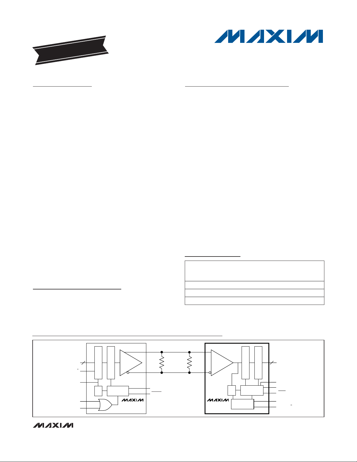
Typical Operating Circuit
Cellular Phone Base
Stations
Add/Drop Muxes
Digital Cross-Connects
DSLAMs
Network Switches and
Routers
Backplane Interconnect
+
Denotes a lead(Pb)-free/RoHS-compliant package.
/V denotes an automotive qualified part.
PART
MAX9206EAI+ -40°C to +85°C 28 SSOP 16 to 40
MAX9206EAI/V+ -40°C to +85°C 28 SSOP 16 to 40
MAX9208EAI+ -40°C to +85°C 28 SSOP 40 to 66
TEMP
RANGE
PINPACKAGE
REF CLOCK
RANGE
(MHz)
BUS
OUT+
10
IN_
TCLK_R/F
TCLK
SYNC 1
SYNC 2
INPUT LATCH
PLL
PARALLEL-TO-SERIAL
TIMING AND
CONTROL
MAX9205
MAX9207
100Ω 100Ω
OUT-
EN
PWRDN
LVDS
PCB OR TWISTED PAIR
RI+
10
ROUT_
RI-
PLL
MAX9206
MAX9208
CLOCK
RECOVERY
OUTPUT LATCH
SERIAL-TO-PARALLEL
TIMING AND
CONTROL
REFCLK
REN
LOCK
RCLK
RCLK_R/F
Page 2
MAX9206/MAX9208
10-Bit Bus LVDS Deserializers
2 _______________________________________________________________________________________
ABSOLUTE MAXIMUM RATINGS
Stresses beyond those listed under “Absolute Maximum Ratings” may cause permanent damage to the device. These are stress ratings only, and functional
operation of the device at these or any other conditions beyond those indicated in the operational sections of the specifications is not implied. Exposure to
absolute maximum rating conditions for extended periods may affect device reliability.
AVCC, DVCC to AGND, DGND................................-0.3V to +4V
RI+, RI- to AGND, DGND .........................................-0.3V to +4V
All Other Pins to DGND..............................-0.3V to DV
CC
+ 0.3V
ROUT_ Short-Circuit Duration (Note 1) ......................Continuous
Continuous Power Dissipation (T
A
= +70°C)
28-Pin SSOP (derate 9.5mW/°C above +70°C) ..........762mW
Operating Temperature Range ...........................-40°C to +85°C
Junction Temperature......................................................+150°C
Storage Temperature Range .............................-65°C to +150°C
ESD Rating (Human Body Model, RI+, RI-) .........................±8kV
Lead Temperature (soldering, 10s) .................................+300°C
Soldering Temperature (reflow) .......................................+260°C
DC ELECTRICAL CHARACTERISTICS
(V
AVCC
= V
DVCC
= +3.0V to +3.6V, differential input voltage |V
ID
| = 0.1V to 1.2V, common-mode voltage V
CM
= |VID/2| to 2.4V
-
|V
ID
/2|, TA= -40°C to +85°C, unless otherwise noted. Typical values are at V
AVCC
= V
DVCC
= +3.3V, VCM= 1.1V, |V
ID
| = 0.2V,
T
A
= +25°C.) (Notes 2, 3)
PARAMETER S YMBOL CONDITIONS MIN TYP MAX UNITS
POWER SUPPLY
CL = 15pF,
Supply Current I
CC
worst-case
pattern,
Figure 1
Power-Down Supply Current I
CCX
PWRDWN = low 1 mA
LVCMOS/LVTTL LOGIC INPUTS (REN, REFCLK, RCLK_R/F, PWRDN)
High-Level Input Voltage VIH 2.0 VCC V
Low-Leve l Input Voltage VIL 0 0.8 V
Input Current I
IN
VIN = 0V, V
AVCC
LVCMOS/LVTTL LOGIC OUTPUTS (ROUT_, RCLK, LOCK)
High-Level Output Voltage VOH IOH = -5mA 2.2 2.9 VCC V
Low-Leve l Output Voltage VOL IOL = 5mA 0 0.33 0.5 V
Output Short-Circuit Current IOS V
Output High-Impedance Current I
OZ
= 0V -15 -38 -85 mA
ROUT_
PWRDN = low, V
= 0V, V
AVCC
, or V
BLVDS S ERIAL INPUT (RI+, RI-)
Differential Input High
Differential Input Low Threshold V
Input Current I
Power-Off Input Current
Input Resistor 1 R
Input Resistor 2 R
9 100 mV
V
TH
-100 -9 mV
TL
0.1V |VID| 0.45V -64 64
, I
RI+
RI-
0.45V < |VID| 0.6V -82 82
I
RI+OFF
I
RI-OFF
0.1V |VID| 0.45V, V
,
0.45V < |VID| 0.6V, V
V
IN1
IN2
AVCC
V
AVCC
= V
= V
DVCC
DVCC
MAX9206
MAX9208
, or V
DVCC
= V
ROUT_
DVCC
AVCC
AVCC
-15 15 μA
RCLK
= V
= V
16MHz 30 45
45MHz 57 75
40MHz 55 75
60MHz 80 100
= V
LOCK
= 0V -64 64
DVCC
= 0V -82 82
DVCC
-1 1 μA
= 3.6V or 0V, Figure 2 4 k
= 3.6V or 0V, Figure 2 150 k
mA
μA
μA
Page 3
MAX9206/MAX9208
10-Bit Bus LVDS Deserializers
_______________________________________________________________________________________ 3
AC ELECTRICAL CHARACTERISTICS
(V
AVCC
= V
DVCC
= +3.0V to +3.6V, CL= 15pF, differential input voltage |V
ID
| = 0.15V to 1.2V, common-mode voltage V
CM
= |VID/2|
to 2.4V - |VID/2|, TA= -40°C to +85°C, unless otherwise noted. Typical values are at V
AVCC
= V
DVCC
= +3.3V, VCM= 1.1V, |V
ID
| =
0.2V, T
A
= +25°C.) (Notes 4, 5)
PARAMETER SYMBOL CONDITIONS MIN TYP MAX UNITS
REFERENCE CLOCK TIMING REQUIREMENTS (REFCLK)
REFCLK Frequency f
RFF
MAX9206 16 45
MAX9208 40 60
REFCLK Frequency Variation RFFV -200 200 ppm
REFCLK Period t
RFCP
MAX9206 22.222 62.500
MAX9208 16.666 25
REFCLK Duty Cycle RFDC 30 50 70 %
REFCLK Input Transition Time t
3 6 ns
RFTT
SWITCHING CHARACTERISTICS
Recovered Clock (RCLK)
Period (Note 6)
Low-to-High Transition Time t
High-to-Low Transition Time t
t
RCP
CLH
CHL
Deserializer Delay tDD Figure 4
ROUT_ Data Valid Before RCLK t
ROUT_ Data Valid After RCLK t
RCLK Duty Cycle t
OUTPUT High-to-High
Impedance Delay
OUTPUT Low-to-High
Impedance Delay
OUTPUT High-Impedance to
High-State Delay
OUTPUT High-Impedance to
Low-State Delay
ROS
ROH
RDC
t
HZR
t
LZR
t
ZHR
t
ZLR
MAX9206 22.222 62.500
MAX9208 16.666 25
Figure 3 1.5 3 ns
Figure 3 2 3 ns
MAX9206, 45MHz
MAX9208, 60MHz
1.75 x t
+ 2
1.75 x t
+ 1.1
Figure 5 0.4 x t
Figure 5 0.4 x t
RCP
RCP
RCP
RCP
1.75 x t
+ 3.3
1.75 x t
+ 3.3
0.5 x t
0.5 x t
RCP
RCP
RCP
RCP
1.75 x t
RCP
+ 6.5
1.75 x t
RCP
+ 5.6
ns
ns
43 50 57 %
CL = 5pF, Figure 6 8 ns
CL = 5pF, Figure 6 8 ns
CL = 5pF, Figure 6 6 ns
CL = 5pF, Figure 6 6 ns
Sync patterns at input; supply and
PLL Lock Time (from PWRDN
Transition High)
t
DSR1
REFCLK stable; measured from
PWRDN transition high to LOCK
(2048 + 42)
x t
RFCP
transition low; Figure 7
MHz
ns
ns
ns
ns
Page 4
MAX9206/MAX9208
Note 1: Short one output at a time. Do not exceed the Absolute Maximum continuous power dissipation.
Note 2: Current into a pin is defined as positive. Current out of a pin is defined as negative. Voltages are referenced to ground
except V
TH
, VTL, and VID, which are differential input voltages.
Note 3: DC parameters are production tested at T
A
= +25°C and guaranteed by design and characterization over operating temper-
ature range.
Note 4: AC parameters guaranteed by design and characterization.
Note 5: C
L
includes scope probe and test jig capacitance.
Note 6: t
RCP
is determined by the period of TCLK, which is the reference clock of the serializer driving the deserializer. The frequen-
cy of TCLK must be within ±400ppm of the REFCLK frequency.
AC ELECTRICAL CHARACTERISTICS (continued)
(V
AVCC
= V
DVCC
= +3.0V to +3.6V, CL= 15pF, differential input voltage |V
ID
| = 0.15V to 1.2V, common-mode voltage V
CM
= |VID/2|
to 2.4V - |VID/2|, TA= -40°C to +85°C, unless otherwise noted. Typical values are at V
AVCC
= V
DVCC
= +3.3V, VCM= 1.1V, |V
ID
| =
0.2V, T
A
= +25°C.) (Notes 4, 5)
10-Bit Bus LVDS Deserializers
4 _______________________________________________________________________________________
PLL Lock Time (from Start of
Sync Patterns)
PARAMETER SYMBOL CONDITIONS MIN TYP MAX UNITS
PLL locked to stable REFCLK; supply
t
DSR2
stable; static input; measured from
start of sync patterns at input to LOCK
transition low; Figure 8
42 x t
RFCP
ns
LOCK High-Z to High-State
Delay
Input Jitter Tolerance tJT Figure 9
t
ZHLK
Figure 7 30 ns
MAX9206
MAX9208
16MHz 1300
45MHz 720
40MHz 720
60MHz 320
ps
Page 5

MAX9206/MAX9208
10-Bit Bus LVDS Deserializers
Pin Description
Figure 1. Worst-Case ICCTest Pattern
Test Circuits/Timing Diagrams
_______________________________________________________________________________________ 5
PIN NAME FUNCTION
1, 12, 13 AGND Analog Ground
Recovered Clock Strobe Edge Select. LVTTL/LVCMOS level input. Drive RCLK_ R/F high to strobe
2 RCLK_R/F
3 REFCLK PLL Reference Clock. LVTTL/LVCMOS level input.
4, 11 AVCC Analog Power Supply. Bypass AVCC with a 0.1μF and a 0.001μF capacitor to AGND.
5 RI+ Serial Data Input. Noninverting BLVDS differential input.
6 RI- Serial Data Input. Inverting BLVDS differential input.
7 PWRDN
8 REN
9 RCLK Recovered Clock. LVTTL/LVCMOS level output. Use RCLK to strobe ROUT_.
10 LOCK
14, 20,
22
15–19,
24–28
DGND Digital Ground
ROUT9–
ROUT0
21, 23 DVCC Digital Power Supply. Bypass DVCC with a 0.1μF and a 0.001μF capacitor to DGND.
ROUT_ on the rising edge of RCLK. Drive RCLK_R/F low to strobe ROUT_ on the falling edge of
RCLK.
Power Down. LVTTL/LVCMOS level input. Drive PWRDN low to stop the PLL and put ROUT_, LOCK,
and RCLK in high impedance.
Output Enable. LVTTL/LVCMOS level input. Drive REN low to put ROUT_ and RCLK in high
impedance. LOCK remains active, indicating the status of the serial input.
Lock Indicator. LVTTL/LVCMOS level output. LOCK goes low when the PLL has achieved frequency
and phase lock to the serial input, and the framing bits have been identified.
Parallel Output Data. LVTTL/LVCMOS level outputs. ROUT_ is valid on the second selected strobe
edge of RCLK after LOCK goes low.
START
BIT
RI
0 0
RCLK
ODD
ROUT
EVEN
ROUT
START
BIT
END
97654321 21
82
BIT
T
DD
RCLK_R/F = HIGH
START
BIT
END
BIT
987654310
Page 6

MAX9206/MAX9208
10-Bit Bus LVDS Deserializers
Figure 5. Data Valid Times
Figure 6. High-Impedance Test Circuit and Timing
Figure 2. Input Fail-Safe Circuit
Figure 3. LVCMOS/LVTTL Output Load and Transition Times
Figure 4. Input-to-Output Delay
Test Circuits/Timing Diagrams (continued)
6 _______________________________________________________________________________________
V
CC
R
IN2
TO DESERIALIZING
CIRCUITRY
R
IN1
VCC - 0.3V
RI+
LVCMOS/LVTTL
OUTPUT
80%
15pF
C
L
80%
R
IN1
RI-
RI
RCLK
ROUT_
RCLK
RCLK_R/F = LOW
RCLK
RCLK_R/F = HIGH
DATA VALID
ROUT_
BEFORE RCLK
START
SYMBOL N
BIT
0123456789 0123456789 012
RCLK_R/F = HIGH
50%
50%
t
ROS
t
ROH
DATA VALID
AFTER RCLK
SYMBOL N-1
t
20%
CHL
20%
t
CLH
START
END
BIT
SYMBOL N+1
BIT
t
DD
SYMBOL N
REN
V
RCLK
OL
V
OH
ROUT_
+7V FOR t
OPEN FOR t
C
L
t
LZR
t
HZR
END
BIT
START
LZR
HZR
BIT
AND t
AND t
500Ω
ZLR
ZHR
450Ω
1.5V
t
ZLR
t
SCOPE
50Ω
ZHR
VOL +0.5V
-0.5V
V
OH
Page 7

MAX9206/MAX9208
10-Bit Bus LVDS Deserializers
_______________________________________________________________________________________ 7
Figure 7. PLL Lock Time from PWRDN
Figure 8. Deserializer PLL Lock Time from
Sync Patterns
Test Circuits/Timing Diagrams (continued)
PWRDN
REFCLK
LOCK
RCLK
ROUT_
RI
HIGH-Z
t
ZHLK
REFCLK
RI
LOCK
t
RFCP
t
RFCP
HIGH-Z
HIGH-Z
2048 x t
t
DSR2
RFCP
t
≤ (2048 + 42)t
DSR1
≤42t
RFCP
RFCP
SYNC PATTERNS
111111
000000
≤42 x t
SYNC PATTERNS
111111
000000
RFCP
DATA
t
DD
t
RCP
DATASYNC
RCLK_R/F = LOW
DATA
DON'T CARE
HIGH-Z
HIGH-Z
HIGH-Z
t
DD
OR t
t
HZR
LZR
RCLK
ROUT_
SYNC
RCLK_R/F = LOW
t
RCP
DATA DATA DATA
Page 8

MAX9206/MAX9208
10-Bit Bus LVDS Deserializers
8 _______________________________________________________________________________________
Detailed Description
The MAX9206/MAX9208 deserialize a BLVDS serializer's output into 10-bit wide parallel LVCMOS/LVTTL
data and a parallel rate clock. The MAX9206/MAX9208
include a PLL that locks to the frequency and phase of
the serial input, and digital circuits that deserialize and
deframe the data. The MAX9206/MAX9208 have highinput jitter tolerance while receiving data at speeds
from 160Mbps to 600Mbps. Combination with the
MAX9205/MAX9207 BLVDS serializers allows data
transmission across backplanes using PCB traces, or
across twin-ax or twisted-pair cables.
The MAX9206/MAX9208 deserializers provide a powersaving, power-down mode when PWRDN is driven low.
The output enable, REN, allows the parallel data outputs (ROUT_) and recovered clock (RCLK) to be
enabled or disabled while maintaining lock to the serial
input. LOCK, along with RCLK, indicates when data is
valid at ROUT_. Parallel, deserialized data at ROUT_ is
strobed out on the selected strobe edge of RCLK. The
strobe edge of RCLK is programmable. The falling
edge is selected when RCLK_R/F is low and the rising
edge is selected when RCLK_R/F is high.
The interface may be point-to-point or a heavily loaded
bus. The characteristic impedance of the media and
connections can range from 100Ω for a point-to-point
interface to 54Ω for a heavily loaded bus. A double-terminated point-to-point interface uses a 100Ω termination resistor at each end of the interface, resulting in a
total load of 50Ω. A heavily loaded bus with a termination as low as 54Ω at each end of the bus (resulting in a
total load of 27Ω) can be driven.
A high state bit and a low state bit, added by the
BLVDS serializer, frame each 10 bits of serial data and
create a guaranteed transition for clock recovery. The
high bit is prepended at the start and the low bit is
appended at the end of the 10-bit data. The rising edge
formed at the end/start bit boundary functions as an
embedded clock. Twelve serial bits (10 data + 2 frame)
are transmitted by the serializer and received by the
deserializer for each 10 bits of data transferred. The
MAX9206 accepts a 16MHz to 45MHz reference clock,
and receives serial data at 160Mbps (10 data bits x
16MHz) to 450Mbps (10 data bits x 45MHz). The
MAX9208 accepts a 40MHz to 60MHz reference clock,
and receives serial data at a rate of 400Mbps to
600Mbps.
Initialization
Initialize the MAX9206/MAX9208 before receiving data.
When power is applied, with REFCLK stable and
PWRDN high, RCLK and ROUT_ are held in high
impedance, LOCK goes high, and the on-chip PLL
locks to REFCLK in 2048 cycles. After locking to REFCLK, ROUT_ is active, RCLK tracks REFCLK, and
LOCK remains high. If transitions are detected at the
serial input, the PLL locks to the phase and frequency
of the serial input, finds the frame bits, and drives
LOCK low. If the serial input is sync patterns, LOCK
goes low in 42 or fewer cycles of RCLK. When LOCK
goes low, RCLK switches from tracking REFCLK to
tracking the serializer reference clock (TCLK).
Deserialized data at ROUT_ is valid on the second
selected strobe edge of RCLK after LOCK goes low.
Initialization restarts when power is cycled or on the rising edge of PWRDN.
Lock to Pseudorandom Data
The MAX9206/MAX9208 lock to pseudorandom serial
input data by deductively eliminating rising edges due
to data until the embedded end/start edge is found.
The end/start edge is identified unless the data contains a permanent, consecutive, frame-to-frame rising
edge at the same bit position. Send sync patterns to
guarantee lock. A sync pattern is six consecutive ones
followed by six consecutive zeros, repeating every
RCLK period with only one rising edge (at the end/start
boundary). The MAX9205/MAX9207 serializers generate sync patterns when SYNC1 or SYNC2 is driven
high.
Since sending sync patterns to initialize a deserializer
disrupts data transfer to all deserializers receiving the
same serial input (Figure 11, for example), lock to
pseudorandom data is preferred in many applications.
Lock to pseudorandom data allows initialization of a
deserializer after hot insertion without disrupting data
communication on other links.
The MAX9206/MAX9208s’ deductive algorithm provides very fast pseudorandom data lock times. Table 1
compares typical lock times for pseudorandom and
sync pattern inputs.
Power-Down
Drive PWRDN low to enter the power-down mode. In
power-down, the PLL is stopped and the outputs
(ROUT_, RCLK, and LOCK) are put in high impedance,
disabling drive current and also reducing supply current.
Output Enable
When the deserializer is initialized and REN is high,
ROUT_ is active, RCLK tracks the serializer reference
clock (TCLK), and LOCK is low. Driving REN low disables the ROUT_ and RCLK output drivers and does
not affect state machine timing. ROUT_ and RCLK go
Page 9

MAX9206/MAX9208
10-Bit Bus LVDS Deserializers
_______________________________________________________________________________________ 9
into high impedance but LOCK continues to reflect the
status of the serial input. Driving REN high again
enables the ROUT_ and RCLK drivers.
Losing Lock on Serial Data
If one embedded clock edge (rising edge formed by
end/start bits) is not detected, LOCK goes high, RCLK
tracks REFCLK, and ROUT_ stays active but with
invalid data. LOCK stays high for a minimum of two
RCLK cycles. Then, if transitions are detected at the
serial input, the PLL attempts to lock to the serial input.
When the PLL locks to serial input data, LOCK goes
low, RCLK tracks the serializer reference clock (TCLK),
and ROUT_ is valid on the second selected strobe
edge of RCLK after LOCK goes low. A minimum of two
embedded clock edges in a row are required to regain
lock to the serial input after LOCK goes high.
For automatic resynchronization, LOCK can be connected to the MAX9205/MAX9207 serializer SYNC1 or
SYNC2 input. With this connection, when LOCK goes
high, the serializer sends sync patterns until the deserializer locks to the serial input and drives LOCK low.
Input Fail-Safe
When the serial input is undriven (a disconnected cable
or serializer output in high impedance, for example) an
on-chip fail-safe circuit (Figure 2) drives the serial input
high. The response time of the fail-safe circuit depends
on interconnect characteristics. With an undriven input,
LOCK may switch high and low until the fail-safe circuit
takes effect. The undriven condition of the link can be
detected in spite of LOCK switching since LOCK is
high long enough to be sampled (LOCK is high for at
least two RCLK cycles after a missed clock edge and
RCLK keeps running, allowing sampling). If it is
required that LOCK remain high for an undriven input,
the on-chip fail-safe circuit can be supplemented with
external pullup bias resistors.
Deserializer Jitter Tolerance
The tJTparameter specifies the total zero-to-peak input
jitter the deserializer can tolerate before a sampling
error occurs (Figure 9). Zero-to-peak jitter is measured
from the mean value of the deterministic jitter distribution. Sources of jitter include the serializer (supply
noise, reference clock jitter, pulse skew, and intersymbol interference), the interconnect (intersymbol interference, crosstalk, within-pair skew, ground shift), and the
deserializer (supply noise). The sum of the zero-to-peak
individual jitter sources must be less than or equal to
the minimum value of t
JT
.
For example, at 40MHz, the MAX9205 serializer has
140ps (p-p) maximum deterministic output jitter. The
zero-to-peak value is 140ps/2 = 70ps. If the interconnect jitter is 100ps (p-p) with a symmetrical distribution,
the zero-to-peak jitter is 50ps. The MAX9206 deserializer jitter tolerance is 720ps at 40MHz. The total zero-topeak input jitter is 70ps + 50ps = 120ps, which is less
than the jitter tolerance. In this case, the margin is
720ps - 120ps = 600ps.
Table 1. Typical Lock Times
Note: Pseudorandom lock performed with 215-1 PRBS pattern, 10,000 lock time tests.
REFCLK
FREQUENCY
DATA
PATTERN
Maximum 0.749μs 0.375μs 0.354μs 0.134μs
Maximum (Clock
Cycles)
Average 0.318μs 0.158μs 0.144μs 0.103μs
Average (Clock
Cycles)
Minimum 0.13μs 0.068μs 0.061μs 0.061μs
Minimum (Clock
Cycles)
16MHz 35MHz 40MHz 40MHz
PSEUDORANDOM
DATA
11.99 13.14 14.18 5.37
5.09 5.52 5.76 4.11
2.08 2.37 2.44 2.45
PSEUDORANDOM
DATA
PSEUDORANDOM
DATA
SYNC
PATTERNS
Page 10
MAX9206/MAX9208
10-Bit Bus LVDS Deserializers
Applications Information
Power-Supply Bypassing
Bypass each supply pin with high-frequency surfacemount ceramic 0.1µF and 0.001µF capacitors in parallel as close to the device as possible, with the smaller
valued capacitor the closest to the supply pin.
Differential Traces and Termination
Trace characteristics affect the performance of the
MAX9206/MAX9208. Use controlled-impedance media.
Avoid the use of unbalanced cables such as ribbon or
simple coaxial cable. Balanced cables such as twisted
pair offer superior signal quality and tend to generate
less EMI due to canceling effects. Balanced cables
tend to pick up noise as common mode, which is
rejected by a differential receiver.
Eliminate reflections and ensure that noise couples as
common mode by running differential traces close
together. Reduce skew by matching the electrical
length of the traces. Excessive skew can result in a
degradation of magnetic field cancellation.
Maintain a constant distance between the differential
traces to avoid discontinuities in differential impedance.
Avoid 90° turns and minimize the number of vias to further prevent impedance discontinuities.
Figure 10. Double-Termination Point-to-Point
Figure 11. Point-to-Point Broadcast Using MAX9150 Repeater
Figure 9. Input Jitter Tolerance
10 ______________________________________________________________________________________
t
/12
RCP
t
JT
t
JT
VID = 150mV
SERIALIZED DATA
PARALLEL
DATA IN
MAX9205
MAX9207
100Ω
100Ω
MAX9206
MAX9208
PARALLEL
DATA OUT
MAX9205
MAX9207
MAX9150
REPEATER
100Ω
ASIC
100Ω
ASIC ASIC
MAX9206
MAX9208
100Ω
100Ω
MAX9206
MAX9208
Page 11

MAX9206/MAX9208
10-Bit Bus LVDS Deserializers
______________________________________________________________________________________ 11
Topologies
The MAX9206/MAX9208 deserializers can operate in a
variety of topologies. Examples of double-terminated
point-to-point and point-to-point broadcast are shown
in Figures 10 and 11. Use 1% surface-mount termination resistors.
A point-to-point interface terminated at each end in the
characteristic impedance of the cable or PCB traces is
shown in Figure 10. The total load seen by the serializer
is 50Ω. The double termination typically reduces reflections compared to a single 100Ω termination. A single
100Ω termination at the deserializer input is feasible
and makes the differential signal swing larger.
A point-to-point version of a multidrop bus is shown in
Figure 11. The low-jitter MAX9150 10-port repeater is
used to reproduce and transmit the serializer output
over 10 double-terminated point-to-point links.
Compared to a bus, more interconnect is traded for
robust hot-plug capability.
The repeater eliminates nine serializers compared to 10
individual point-to-point serializer-to-deserializer connections. Since repeater jitter is a component of the
total jitter seen at the deserializer input (along with
other sources of jitter), a low-jitter repeater is essential
in most high data-rate applications.
Board Layout
A four-layer PCB providing separate power, ground,
and signal layers is recommended. Keep the
LVTTL/LVCMOS inputs and outputs separated from the
BLVDS inputs to prevent coupling into the BLVDS lines.
Chip Information
PROCESS: CMOS
Table 2. Input/Output Function Table
X = Don’t care.
Pin Configuration
PACKAGE
TYPE
PACKAGE
CODE
OUTLINE
NO.
LAND
PATTERN NO.
28 SSOP A28+4
21-0056 90-0095
Package Information
For the latest package outline information and land patterns,
go to www.maxim-ic.com/packages
. Note that a “+”, “#”, or
“-” in the package code indicates RoHS status only. Package
drawings may show a different suffix character, but the drawing
pertains to the package regardless of RoHS status.
LOGIC INPUTS
REN PWRDN
X Low Power applied and stable
Low High Deserializer initialized
High High Deserializer initialized
CONDITIONS OUTPUTS
Power-down mode. PLL is stopped. Current consumption is reduced
to 400μA (typ). ROUT_, RCLK, and LOCK are high impedance.
RCLK and ROUT_ are high impedance. LOCK is active, indicating
the serial input status.
RCLK and ROUT_ are active. LOCK is active, indicating the serial
input status.
TOP VIEW
AGND
RCLK_R/F
REFCLK
AVCC
PWRDN
REN
RCLK
LOCK
AVCC
AGND
AGND
DGND
+
1
2
3
4
RI+
5
10
11
12
13
14
6
7
8
9
MAX9206/
MAX9208
SSOP
RI-
ROUT0
28
ROUT1
27
ROUT2
26
ROUT3
25
ROUT4
24
DVCC
23
DGND
22
DVCC
21
DGND
20
ROUT5
19
ROUT6
18
ROUT7
17
ROUT8
16
ROUT9
15
Page 12
MAX9206/MAX9208
10-Bit Bus LVDS Deserializers
Maxim cannot assume responsibility for use of any circuitry other than circuitry entirely embodied in a Maxim product. No circuit patent licenses are implied.
Maxim reserves the right to change the circuitry and specifications without notice at any time.
12
____________________Maxim Integrated Products, 120 San Gabriel Drive, Sunnyvale, CA 94086 408-737-7600
© 2010 Maxim Integrated Products Maxim is a registered trademark of Maxim Integrated Products, Inc.
Revision History
REVISION
NUMBER
0 8/01 Initial release —
1 12/07
2 11/10 Updated Ordering Information, Absolute Maximum Ratings, and Package Information 1, 2, 12
REVISION
DATE
DESCRIPTION
Max clock frequency increased to 45MHz; min values decreased for REFCLK and
RCLK period; updated package outline; updated names for pins 2 and 3.
PAGES
CHANGED
1–5, 8, 12
 Loading...